full-text - Radioengineering
full-text - Radioengineering
full-text - Radioengineering

You also want an ePaper? Increase the reach of your titles
YUMPU automatically turns print PDFs into web optimized ePapers that Google loves.
68 V. ŠÁDEK, THE CONFORMAL CORRECTION IN THE STRIP-CENTERED COAXIAL LINE ANALYSIS<br />
The Conformal Correction<br />
in the Strip-Centered Coaxial Line Analysis<br />
Václav ŠÁDEK<br />
Dept. of Theoretical and Exp. El. Engineering, Brno Univ. of Technology Kolejní 2906/4, 612 00 Brno, Czech Republic<br />
sadek@feec.vutbr.cz<br />
Abstract. The presented work reports on the novel analysis<br />
of the strip-centered coaxial line. The conformal mapping<br />
method is used.<br />
For a narrow central strip a very easy conformal mapping<br />
is described that maps this structure onto the rectangular<br />
model line, but great distortion for wide strip inhibits application<br />
of this mapping in all the extent. The conformal<br />
mapping method allows to correct this fault very smartly<br />
by extension in auxiliary plane.<br />
Two different numerical models are also mentioned as<br />
comparative solutions of strip-centered coaxial line analysis.<br />
One of them is based on numerical evaluating of the<br />
Schwarz-Christoffel integral, the other (in two modifications)<br />
is based on boundary element method (BEM).<br />
Keywords<br />
Strip-centered coaxial line, characteristic impedance,<br />
conformal mapping, conformal correction, numerical<br />
solution of Schwarz-Christoffel integral, BEM.<br />
1. Introduction<br />
A great boom of numerical method does not decrease<br />
the main advantage of the analytical methods - one mathematical<br />
function describes physical model. While in case of<br />
some numerical method we have to start whole analysis<br />
every time we change any parameter, analytical solution<br />
gives us result as quickly as we can enumerate one mathematical<br />
function. Also the influence of each particular<br />
parameter is clear from analytical solution, but not from<br />
every set of numerical results.<br />
A lot of different electronic equipments have to work<br />
together. Unfortunately the power levels among them are<br />
over 200 dB very often. Coaxial structures are widely used<br />
because of their good shielding effect, which suppress the<br />
fields around strong distortion sources (e.g. transmitting<br />
antenna feeder) and protect sensitive parts of receivers,<br />
measurement inputs of the equipments etc. [1], [2].<br />
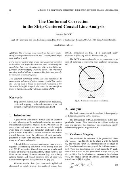
Whereas coaxial line (two concentric cylindrical<br />
electrodes) is widely known, strip-centered coaxial line<br />
(SCCL, normalized on Fig. 1.) is mentioned rarely<br />
(founded only in very special literature like [3]).<br />
The SCCL structure also offers a very attractive occasion<br />
of matching to microstrip line, coplanar waveguide,<br />
etc.<br />
1<br />
2. Analysis<br />
2z<br />
Fig. 1. Normalized strip-centered coaxial line.<br />
The basic assumption of the analysis is homogeneity<br />
of dielectric across the SCCL structure.<br />
The arrangement of SCCL is symmetrical in two perpendicular<br />
planes. That convenient fact allows analyzing<br />
only one quarter of this structure. The open cuts are simply<br />
substituted by perfect magnetic walls.<br />
2.1 Conformal Mapping<br />
Let us assume the existence of the generalized triangle<br />
(w 1 w 3 w 4 - see Fig. 2b) in the plane w with the height<br />
π/2 and with one vertex (w 1 ) in infinity and let the origin of<br />
the Cartesian coordinates merge with the left bottom vertex<br />
(w 4 ). There is a transform z→w, which maps the 1 st quadrant<br />
of the plane z to this generalized triangle w 1 w 3 w 4 on<br />
the condition that the abscissa z 3 z 4 maps onto the abscissa<br />
w 3 w 4 . The special version of Schwarz-Christoffel mapping<br />
(mentioned in [4]) is applied<br />
dw<br />
2<br />
dz<br />
1<br />
2 −<br />
( ) 1<br />
2<br />
2 2 −<br />
z ( z − ) 2<br />
= z<br />
4<br />
4<br />
. (1)
RADIOENGINEERING, VOL. 16, NO. 3, SEPTEMBER 2007 69<br />
All the symbols are in agreement with Fig. 1. and<br />
Fig. 2. The integral of this expression takes us the transform<br />
formula<br />
w = arccosh( z z 4<br />
). (2)<br />
What happens with the surrounding electrode (arc<br />
z 2 z 5 )? This arc maps itself onto a curve w 2 w 5 . In case of<br />
very small z 4 this curve is very close to abscissa orthogonal<br />
to x-axis. This could be a solution of the task, the characteristic<br />
impedance of the SCCL is proportional to the position<br />
of the point w 5 (in (8) w 5 instead of w d 5 ) but for other<br />
z 4 , greater than 0.2 (approx.), the difference between the<br />
ideal abscissa and our curve is not acceptable unfortunately.<br />
The correction has to be applied and the conformal<br />
method offers a very attractive way.<br />
a)<br />
b)<br />
c)<br />
d)<br />
j<br />
z =0<br />
3<br />
jπ<br />
2<br />
z<br />
2<br />
w =0 w<br />
4 5<br />
z<br />
1<br />
z z<br />
4 5<br />
w3<br />
p3<br />
1<br />
(z)<br />
b<br />
(w )<br />
w<br />
2<br />
(p)<br />
p =0 p p 1 p<br />
4 5<br />
2<br />
jπ<br />
2<br />
w3<br />
d b<br />
w2<br />
w =0 w<br />
4 5<br />
w 1<br />
d<br />
(w )<br />
w 1<br />
Fig. 2. Conformal mapping and correction.<br />
2.2 Conformal Correction<br />
The idea of the conformal correction (CC) is to<br />
transform our plane w to an auxiliary plane p and return<br />
back, but “little bit” modified.<br />
For the sake of clarity, we rename our plane w<br />
(Fig. 2b) to w b and the corrected plane w (Fig. 2d) to w d . In<br />
the plane p the mark b relates to the plane p before adjustment<br />
and the mark d after it.<br />
In Svačina’s work [4] there is the identical shape to<br />
our shape in the plane w b . There it is used as the conformal<br />
map of the circular wire over a flat plane (approximation of<br />
a narrow microstrip). Because we interchange the cause<br />
and the result and transform the shape on the plane w b to<br />
a “wire-over-plate” line, we use an inverse transform<br />
b<br />
p= tanh w . (3)<br />
The infinity point w 1 b →∞ maps itself onto the point p 1 b .<br />
Now let us assume the arc p 2 p 5 is circular (it is not, in fact,<br />
but the difference is marginal). In [5] there is the method of<br />
a circular wire over a flat plane described. It consists of<br />
two steps. The first of them is a scaling (see below) and the<br />
second one is an inverse transform to (3) – regress back to<br />
the plane w<br />
d<br />
d<br />
w = arctanh p . (4)<br />
The whole magic is in a smart scaling. The requested result<br />
we will get if the point p 1 d →w 1 d →∞ is the geometrical<br />
average value of p 2 p 5<br />
p<br />
= p p , (5)<br />
b<br />
1 2 5<br />
but the point w 1 d →∞ is the map (4) of the point p 1 d = 1. So<br />
if we adjust the plane p b by division by p 1 b , we get the<br />
plane p d we have wanted<br />
d b b<br />
p = p p . (6)<br />
1<br />
We can say we stretch the shape in the plane p b by the<br />
factor 1/p b 1 to get the shape in the plane p d .<br />
The described method corrects the main distortion<br />
of the rectangular shape of our structure in the plane w.<br />
Because the arc p 2 p 5 is not exactly a half circle, the curve<br />
w d 2 w d 5 is not a straight abscissa, but the deviation is neglectable<br />
(except the limit case when z 4 is very close to 1).<br />
2.3 The Application of CC on SCCL<br />
Let us have "an ideal transmission line" - the rectangle<br />
with two opposite electrodes made from PEC (their<br />
proportion is y) and with the rest sides (proportion x) made<br />
from PMC. The direction of the electrical field intensity<br />
vector is perpendicular to electrodes and the vector of<br />
magnetic field intensity is parallel to them (Fig. 3.). The<br />
field inside the rectangle is homogenous. The characteristic<br />
wave impedance is<br />
Ex<br />
⋅ x 120π x<br />
Z0 = = . (7)<br />
H ⋅ y ε y<br />
y<br />
r<br />
The shape on Fig. 2.d is approximately such a structure<br />
with x = w 5 d and y = π /2, but because we use only one<br />
quarter of the whole cross section for the analysis and all<br />
four quarters are connected "in parallel" in <strong>full</strong> cross section<br />
of the SCCL, the true characteristic impedance value is<br />
4 times smaller
70 V. ŠÁDEK, THE CONFORMAL CORRECTION IN THE STRIP-CENTERED COAXIAL LINE ANALYSIS<br />
Z<br />
0<br />
d<br />
1 120 π w5<br />
60 d<br />
= = w . (8)<br />
5<br />
4 ε 0.5π<br />
r<br />
ε r<br />
Z<br />
0<br />
60 1 − z<br />
= arctanh . (14)<br />
ε z<br />
4<br />
1 +<br />
r<br />
2<br />
4<br />
2<br />
4<br />
y<br />
E<br />
x<br />
H<br />
y<br />
3. Numerical Solution<br />
Because the SCCL is not a commonly used structure,<br />
it is very difficult to verify the results of the described<br />
analysis. That is the reason why two different numerical<br />
models are used.<br />
Fig. 3. Ideal transmission line (thick line: PEC, thin line: PMC).<br />
The aim of the next paragraph is to find a formula for the<br />
description of w 5 d . From (2) - (6) we get<br />
w<br />
w<br />
p<br />
p<br />
p<br />
w<br />
z<br />
j<br />
= arccosh = arccosh ,<br />
b 2<br />
2<br />
z4 z4<br />
z 1<br />
= arccosh = arccosh ,<br />
b 5<br />
5<br />
z4 z4<br />
b<br />
b<br />
2<br />
= tanh w2,<br />
b<br />
b<br />
5<br />
= tanh w5,<br />
b<br />
b<br />
d p5 p5<br />
5<br />
= = ,<br />
b b b<br />
p2p<br />
p<br />
5 2<br />
d<br />
d<br />
5<br />
= arctanh p5.<br />
The formulae (9a) and (9b) after the substitution<br />
x<br />
2<br />
− 1<br />
arccosh x = arctanh ;<br />
x<br />
and some derivations are<br />
w<br />
w<br />
= arctanh 1 + z ,<br />
b 2<br />
2 4<br />
= arctanh 1 −z<br />
.<br />
b 2<br />
5 4<br />
So in the plane p b we get<br />
p = 1 + z ,<br />
b 2<br />
2 4<br />
p = 1 −z<br />
.<br />
b 2<br />
5 4<br />
x<br />
1<br />
x =<br />
z<br />
4<br />
After the CC (9e) the point p 5 b moves to<br />
p<br />
1−<br />
z 1<br />
2 2<br />
d 4 − z4<br />
4<br />
5<br />
= =<br />
2<br />
2<br />
1+<br />
z 1+<br />
z<br />
4<br />
4<br />
Transform (4) gives us the location of the point w 5<br />
d<br />
w<br />
1−<br />
z<br />
arctanh arctanh 1<br />
2<br />
d d 4<br />
4<br />
5<br />
= p5 =<br />
2<br />
+ z4<br />
.<br />
(9a-f)<br />
(10a, b)<br />
(11a, b)<br />
(12)<br />
. (13)<br />
and the installation of (13) into (8) faces to characteristic<br />
impedance formula of the SCCL<br />
3.1 Numerical Solution of<br />
Schwarz-Christoffel Integral<br />
This method is based on the same theoretical basis as<br />
above presented solution, but solved numerically.<br />
A practical tool for numerical Schwarz-Christoffel<br />
integral enumeration is the sc-toolbox [6] for Matlab ® .<br />
Because of this toolbox works only with straight lines, the<br />
arc z 2 z 5 is approximated by a piecewise broken line.<br />
List of main part of the m-file:<br />
a=linspace(0, –i*pi/2,N)';<br />
p=polygon([0; z4; exp(a)]);<br />
f=rectmap(p,[1 2 3 length(p)]);<br />
m=modulus(f);<br />
Zsc=30*pi/m;<br />
The symbol z4 means the half width of the strip z 4 according<br />
to Fig. 2 and N is the number of broken line pieces. In<br />
the enumeration the value N = 20 was selected.<br />
3.2 Boundary Element Method<br />
The boundary element method (BEM) [7] is based on<br />
integral Maxwell’s equations (Laplace’s equation is solved<br />
along the boundary of the structure only). We need values<br />
of the field intensity just along PEC’s for characteristic<br />
impedance determination according to the formula below:<br />
z<br />
∫ E dy<br />
4<br />
Z<br />
0<br />
= = 30π U ∫ E y<br />
dx<br />
(15)<br />
H dx<br />
∫<br />
0<br />
where U is the voltage between conductors and E y is the<br />
electric field y-component along the central electrode. (The<br />
integrals in the first fraction are only informative; they both<br />
are not displayed in the exact form)<br />
The boundary z 2 z 3 z 4 z 5 (Fig. 2a) is divided into boundary<br />
elements, with Dirichlet’s condition along PEC and<br />
Neumann’s condition along PMC. The vectors of potentials<br />
in all boundary elements and the vectors of their gradients<br />
(both vectors partly known and partly not known)<br />
are mutually tied by two matrices H and G, built up according<br />
the rules of BEM.<br />
The task was solved in Matlab ® again. Two different<br />
strategies were tested.
RADIOENGINEERING, VOL. 16, NO. 3, SEPTEMBER 2007 71<br />
The first of them is based on a constant number of<br />
boundary elements (n = 50) per one basic element. The flat<br />
inner electrode is divided into n = 50 elements, the round<br />
outer electrode is divided also into n = 50 elements and<br />
both the magnetic walls are also divided each into n = 50<br />
pieces. That means the total sum of all boundary elements<br />
is 4n = 200. The lengths of elements are not the same,<br />
especially in case of z 4 ≠ 0.5.<br />
The second strategy is based on equidistant division<br />
of the border (except the outer electrode). The inner electrode<br />
is divided to z 4 times n pieces, the continuing magnetic<br />
wall into (1- z 4 ) times n pieces, the outer electrode<br />
into n elements and the last magnetic wall also into n elements.<br />
On the ground of calculation in a wide range of z 4 ,<br />
the number of elements was n = 100.<br />
z 4<br />
This<br />
work<br />
0.01 317.89<br />
0<br />
0.05 221.33<br />
0<br />
0.1 179.74<br />
0<br />
0.2 138.14<br />
0.01<br />
0.3 113.75<br />
0.07<br />
0.4 96.32<br />
0.25<br />
0.5 82.58<br />
0.06<br />
0.6 70.95<br />
0.34<br />
0.7 60.47<br />
0.83<br />
0.8 50.25<br />
1.89<br />
0.9 38.78<br />
4.71<br />
0.95 31.05<br />
8.62<br />
0.99 19.67<br />
20.45<br />
Z 0 [Ω] / error [%]<br />
Wadell<br />
[3]<br />
sc–<br />
toolbox<br />
317.89 317.86<br />
0.01<br />
221.33 221.31<br />
0.02<br />
179.74 179.71<br />
0.02<br />
138.16 138.11<br />
0.03<br />
113.83 113.73<br />
0.08<br />
96.57 96.34<br />
0.24<br />
82.63 82.66<br />
0.04<br />
71.19 71.17<br />
0.03<br />
60.98 60.94<br />
0.06<br />
51.22 51.17<br />
0.08<br />
40.70 40.64<br />
0.15<br />
33.98 33.89<br />
0.25<br />
24.73 24.57<br />
0.64<br />
BEM-1<br />
651.46<br />
105<br />
273.26<br />
23.46<br />
206.83<br />
15.07<br />
152.71<br />
10.53<br />
122.83<br />
7.52<br />
96.53<br />
0.03<br />
82.89<br />
0.32<br />
71.42<br />
0.32<br />
60.98<br />
0.38<br />
51.48<br />
0.50<br />
41.03<br />
0.81<br />
34.44<br />
1.35<br />
26.14<br />
5.71<br />
Tab. 1. Results of analysis (error compared to Wadell [3]).<br />
4. Results<br />
BEM-2<br />
323.41<br />
1.73<br />
223.21<br />
0.85<br />
180.75<br />
0.55<br />
138.64<br />
0.35<br />
114.10<br />
0.25<br />
96.63<br />
0.06<br />
82.91<br />
0.34<br />
71.39<br />
0.28<br />
61.15<br />
0.28<br />
51.38<br />
0.32<br />
40.89<br />
0.48<br />
34.24<br />
0.76<br />
25.39<br />
2.68<br />
Results of all methods are displayed in Tab. 1.<br />
Since this work focuses on SCCL analysis without<br />
a special analysis of the dielectric substrate (homogeneity<br />
assumption), results were calculated for free space (ε r = 1).<br />
All results are compared to the relevant results of the<br />
method mentioned in Wadell’s book [3], however he does<br />
not inform about the accuracy of the mentioned formula.<br />
He only cites his sources – Bongianni [8] and Hilberg [9].<br />
Bongianni made an experiment which confirms this<br />
method (the accuracy is in range of measurement errors),<br />
Hilberg [9] is the author of this method, but he only<br />
describes it, not comparing to any other method. But only<br />
these results [3] (and also the same in [8] and [9]) are independent<br />
on the author of this work.<br />
5. Conclusion<br />
One method founded in literature [3] is easy, but with<br />
the chicken-to-egg problem of choosing one of two formulae<br />
according to their results.<br />
The designed method has no chicken-to-egg problem,<br />
but it is little bit complicated in mathematical way - it contains<br />
the biquadratic root and arc-hyperbolic function.<br />
The error of the designed method compared to [3] is<br />
very small, grows only for z 4 very close to 1. The reason of<br />
this error is in curveting of the wall w 2 w 5 which grows for<br />
z 4 → 1 (see Fig. 2.d). In consequence of nonzero thickness<br />
of the inner conductor the reliability of all methods in this<br />
region is pure. Moreover the characteristic impedance of<br />
the real structure is in this case smaller than the result of<br />
[3] (nonzero thickness of the central strip) and the described<br />
method results are also smaller. They are maybe<br />
mathematically incorrect, but more in consonance of<br />
physical reality.<br />
Acknowledgement<br />
The author would like to express his thanks to<br />
prof. J. Svačina for revision and support, prof. Z. Raida for<br />
help with BEM, J. Dřínovský and T. Urbanec for reference<br />
searching and a lot of other people for encouragement.<br />
References<br />
[1] SVAČINA, J. Electromagnetic Compatibility – lectures. Textbook of<br />
the Brno University of Technology, FEKT VUT Brno, 2002.<br />
[2] ARMSTRONG, K. Design Techniques for EMC.<br />
http://www.compliance-club.com/keith_armstrong.asp<br />
[3] WADELL, B. C. Transmission Line Design Handbook. Boston-<br />
London: Artech House, 1991.<br />
[4] SVAČINA, J. Investigation of Hybrid Microwave Integrated Circuits<br />
by a Conformal Mapping Method). Brno Univ. of Technology, A-46,<br />
Brno, 1991 (in Czech).<br />
[5] ŠÁDEK, V. Analysis of the two-wire transmission line by a conformal<br />
mapping method. In Proc. of Radioelektronika, Bratislava 2002.<br />
[6] DRISCOLL, T. A. SC-Tolbox, for MATLAB.<br />
http://www.math.edu/~driscoll/SC/<br />
[7] PARIS, F., CANAS, J. Boundary Element Method. Oxford: Oxford<br />
University Press, 1997.<br />
[8] BONGIANNI, W. L. Fabrication and performance of strip-centered<br />
microminiature coaxial cable. In Proceeding of the IEEE, 1984, vol.<br />
72, no. 12, p. 1810-1811.<br />
[9] HILBERG, W. Electric Characteristics of Transmission Lines.<br />
Dedham, MA: Artech House, 1979, p. 122.