full-text - Radioengineering
full-text - Radioengineering
full-text - Radioengineering

Create successful ePaper yourself
Turn your PDF publications into a flip-book with our unique Google optimized e-Paper software.
RADIOENGINEERING, VOL. 16, NO. 3, SEPTEMBER 2007 69<br />
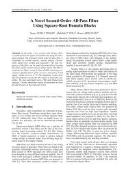
All the symbols are in agreement with Fig. 1. and<br />
Fig. 2. The integral of this expression takes us the transform<br />
formula<br />
w = arccosh( z z 4<br />
). (2)<br />
What happens with the surrounding electrode (arc<br />
z 2 z 5 )? This arc maps itself onto a curve w 2 w 5 . In case of<br />
very small z 4 this curve is very close to abscissa orthogonal<br />
to x-axis. This could be a solution of the task, the characteristic<br />
impedance of the SCCL is proportional to the position<br />
of the point w 5 (in (8) w 5 instead of w d 5 ) but for other<br />
z 4 , greater than 0.2 (approx.), the difference between the<br />
ideal abscissa and our curve is not acceptable unfortunately.<br />
The correction has to be applied and the conformal<br />
method offers a very attractive way.<br />
a)<br />
b)<br />
c)<br />
d)<br />
j<br />
z =0<br />
3<br />
jπ<br />
2<br />
z<br />
2<br />
w =0 w<br />
4 5<br />
z<br />
1<br />
z z<br />
4 5<br />
w3<br />
p3<br />
1<br />
(z)<br />
b<br />
(w )<br />
w<br />
2<br />
(p)<br />
p =0 p p 1 p<br />
4 5<br />
2<br />
jπ<br />
2<br />
w3<br />
d b<br />
w2<br />
w =0 w<br />
4 5<br />
w 1<br />
d<br />
(w )<br />
w 1<br />
Fig. 2. Conformal mapping and correction.<br />
2.2 Conformal Correction<br />
The idea of the conformal correction (CC) is to<br />
transform our plane w to an auxiliary plane p and return<br />
back, but “little bit” modified.<br />
For the sake of clarity, we rename our plane w<br />
(Fig. 2b) to w b and the corrected plane w (Fig. 2d) to w d . In<br />
the plane p the mark b relates to the plane p before adjustment<br />
and the mark d after it.<br />
In Svačina’s work [4] there is the identical shape to<br />
our shape in the plane w b . There it is used as the conformal<br />
map of the circular wire over a flat plane (approximation of<br />
a narrow microstrip). Because we interchange the cause<br />
and the result and transform the shape on the plane w b to<br />
a “wire-over-plate” line, we use an inverse transform<br />
b<br />
p= tanh w . (3)<br />
The infinity point w 1 b →∞ maps itself onto the point p 1 b .<br />
Now let us assume the arc p 2 p 5 is circular (it is not, in fact,<br />
but the difference is marginal). In [5] there is the method of<br />
a circular wire over a flat plane described. It consists of<br />
two steps. The first of them is a scaling (see below) and the<br />
second one is an inverse transform to (3) – regress back to<br />
the plane w<br />
d<br />
d<br />
w = arctanh p . (4)<br />
The whole magic is in a smart scaling. The requested result<br />
we will get if the point p 1 d →w 1 d →∞ is the geometrical<br />
average value of p 2 p 5<br />
p<br />
= p p , (5)<br />
b<br />
1 2 5<br />
but the point w 1 d →∞ is the map (4) of the point p 1 d = 1. So<br />
if we adjust the plane p b by division by p 1 b , we get the<br />
plane p d we have wanted<br />
d b b<br />
p = p p . (6)<br />
1<br />
We can say we stretch the shape in the plane p b by the<br />
factor 1/p b 1 to get the shape in the plane p d .<br />
The described method corrects the main distortion<br />
of the rectangular shape of our structure in the plane w.<br />
Because the arc p 2 p 5 is not exactly a half circle, the curve<br />
w d 2 w d 5 is not a straight abscissa, but the deviation is neglectable<br />
(except the limit case when z 4 is very close to 1).<br />
2.3 The Application of CC on SCCL<br />
Let us have "an ideal transmission line" - the rectangle<br />
with two opposite electrodes made from PEC (their<br />
proportion is y) and with the rest sides (proportion x) made<br />
from PMC. The direction of the electrical field intensity<br />
vector is perpendicular to electrodes and the vector of<br />
magnetic field intensity is parallel to them (Fig. 3.). The<br />
field inside the rectangle is homogenous. The characteristic<br />
wave impedance is<br />
Ex<br />
⋅ x 120π x<br />
Z0 = = . (7)<br />
H ⋅ y ε y<br />
y<br />
r<br />
The shape on Fig. 2.d is approximately such a structure<br />
with x = w 5 d and y = π /2, but because we use only one<br />
quarter of the whole cross section for the analysis and all<br />
four quarters are connected "in parallel" in <strong>full</strong> cross section<br />
of the SCCL, the true characteristic impedance value is<br />
4 times smaller