LMC6081 Precision CMOS Single Operational Amplifier
LMC6081 Precision CMOS Single Operational Amplifier
LMC6081 Precision CMOS Single Operational Amplifier

Create successful ePaper yourself
Turn your PDF publications into a flip-book with our unique Google optimized e-Paper software.
<strong>LMC6081</strong><br />
<strong>Precision</strong> <strong>CMOS</strong> <strong>Single</strong> <strong>Operational</strong> <strong>Amplifier</strong><br />
General Description<br />
The <strong>LMC6081</strong> is a precision low offset voltage operational<br />
amplifier, capable of single supply operation. Performance<br />
characteristics include ultra low input bias current, high voltage<br />
gain, rail-to-rail output swing, and an input common<br />
mode voltage range that includes ground. These features,<br />
plus its low offset voltage, make the <strong>LMC6081</strong> ideally suited<br />
for precision circuit applications.<br />
Other applications using the <strong>LMC6081</strong> include precision fullwave<br />
rectifiers, integrators, references, and sample-andhold<br />
circuits.<br />
This device is built with National’s advanced Double-Poly<br />
Silicon-Gate <strong>CMOS</strong> process.<br />
For designs with more critical power demands, see the<br />
LMC6061 precision micropower operational amplifier.<br />
For a dual or quad operational amplifier with similar features,<br />
see the LMC6082 or LMC6084 respectively.<br />
PATENT PENDING<br />
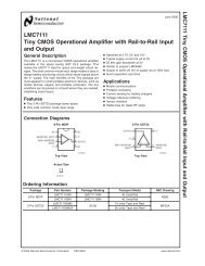
Connection Diagram<br />
8-Pin DIP/SO<br />
Features<br />
(Typical unless otherwise stated)<br />
n Low offset voltage: 150 µV<br />
n Operates from 4.5V to 15V single supply<br />
n Ultra low input bias current: 10 fA<br />
n Output swing to within 20 mV of supply rail, 100k load<br />
n Input common-mode range includes V −<br />
n High voltage gain: 130 dB<br />
n Improved latchup immunity<br />
Applications<br />
n Instrumentation amplifier<br />
n Photodiode and infrared detector preamplifier<br />
n Transducer amplifiers<br />
n Medical instrumentation<br />
n D/A converter<br />
n Charge amplifier for piezoelectric transducers<br />
Low-Leakage Sample and Hold<br />
August 2000<br />
<strong>LMC6081</strong> <strong>Precision</strong> <strong>CMOS</strong> <strong>Single</strong> <strong>Operational</strong> <strong>Amplifier</strong><br />
Top View<br />
01142301<br />
01142312<br />
© 2004 National Semiconductor Corporation DS011423 www.national.com
<strong>LMC6081</strong><br />
Absolute Maximum Ratings (Note 1)<br />
If Military/Aerospace specified devices are required,<br />
please contact the National Semiconductor Sales Office/<br />
Distributors for availability and specifications.<br />
Differential Input Voltage<br />
±Supply Voltage<br />
Voltage at Input/Output Pin<br />
(V + ) +0.3V,<br />
(V − ) −0.3V<br />
Supply Voltage (V + −V − )<br />
16V<br />
Output Short Circuit to V + (Note 10)<br />
Output Short Circuit to V − (Note 2)<br />
Lead Temperature<br />
(Soldering, 10 Sec.)<br />
260˚C<br />
Storage Temp. Range<br />
−65˚C to +150˚C<br />
Junction Temperature<br />
150˚C<br />
ESD Tolerance (Note 4)<br />
2 kV<br />
Current at Input Pin<br />
±10 mA<br />
Current at Output Pin<br />
±30 mA<br />
Current at Power Supply Pin<br />
40 mA<br />
Power Dissipation (Note 3)<br />
Operating Ratings (Note 1)<br />
Temperature Range<br />
<strong>LMC6081</strong>AM<br />
−55˚C ≤ T J ≤<br />
+125˚C<br />
−40˚C ≤ T J ≤ +85˚C<br />
<strong>LMC6081</strong>AI, <strong>LMC6081</strong>I<br />
Supply Voltage 4.5V ≤ V + ≤ 15.5V<br />
Thermal Resistance (θ JA ), (Note 11)<br />
N Package, 8-Pin Molded DIP<br />
115˚C/W<br />
M Package, 8-Pin Surface<br />
Mount<br />
Power Dissipation (Note 9)<br />
193˚C/W<br />
DC Electrical Characteristics<br />
Unless otherwise specified, all limits guaranteed for T J = 25˚C. Boldface limits apply at the temperature extremes. V + = 5V, V −<br />
= 0V, V CM = 1.5V, V O = 2.5V and R L<br />
> 1M unless otherwise specified.<br />
Typ <strong>LMC6081</strong>AM <strong>LMC6081</strong>AI <strong>LMC6081</strong>I<br />
Symbol Parameter Conditions (Note 5) Limit Limit Limit Units<br />
(Note 6) (Note 6) (Note 6)<br />
V OS Input Offset Voltage 150 350 350 800 µV<br />
1000 800 1300 Max<br />
TCV OS Input Offset Voltage 1.0 µV/˚C<br />
Average Drift<br />
I B Input Bias Current 0.010 pA<br />
100 4 4 Max<br />
I OS Input Offset Current 0.005 pA<br />
100 2 2 Max<br />
R IN Input Resistance >10 Tera Ω<br />
CMRR Common Mode 0V ≤ V CM ≤ 12.0V 85 75 75 66 dB<br />
Rejection Ratio V + = 15V 72 72 63 Min<br />
+PSRR Positive Power Supply 5V ≤ V + ≤ 15V 85 75 75 66 dB<br />
Rejection Ratio V O = 2.5V 72 72 63 Min<br />
−PSRR Negative Power Supply 0V ≤ V − ≤ −10V 94 84 84 74 dB<br />
Rejection Ratio 81 81 71 Min<br />
V CM Input Common-Mode V + = 5V and 15V −0.4 −0.1 −0.1 −0.1 V<br />
Voltage Range for CMRR ≥ 60 dB 0 0 0 Max<br />
V + − 1.9 V + − 2.3 V + − 2.3 V + − 2.3 V<br />
V + − 2.6 V + − 2.5 V + − 2.5 Min<br />
A V Large Signal R L =2kΩ Sourcing 1400 400 400 300 V/mV<br />
Voltage Gain (Note 7) 300 300 200 Min<br />
Sinking 350 180 180 90 V/mV<br />
70 100 60 Min<br />
R L = 600Ω Sourcing 1200 400 400 200 V/mV<br />
(Note 7) 150 150 80 Min<br />
Sinking 150 100 100 70 V/mV<br />
35 50 35 Min<br />
www.national.com 2
DC Electrical Characteristics (Continued)<br />
Unless otherwise specified, all limits guaranteed for T J = 25˚C. Boldface limits apply at the temperature extremes. V + = 5V, V −<br />
= 0V, V CM = 1.5V, V O = 2.5V and R L<br />
> 1M unless otherwise specified.<br />
Typ <strong>LMC6081</strong>AM <strong>LMC6081</strong>AI <strong>LMC6081</strong>I<br />
Symbol Parameter Conditions (Note 5) Limit Limit Limit Units<br />
(Note 6) (Note 6) (Note 6)<br />
V O Output Swing V + = 5V 4.87 4.80 4.80 4.75 V<br />
R L =2kΩ to 2.5V 4.70 4.73 4.67 Min<br />
0.10 0.13 0.13 0.20 V<br />
0.19 0.17 0.24 Max<br />
V + = 5V 4.61 4.50 4.50 4.40 V<br />
R L = 600Ω to 2.5V 4.24 4.31 4.21 Min<br />
0.30 0.40 0.40 0.50 V<br />
0.63 0.50 0.63 Max<br />
V + = 15V 14.63 14.50 14.50 14.37 V<br />
R L =2kΩ to 7.5V 14.30 14.34 14.25 Min<br />
0.26 0.35 0.35 0.44 V<br />
0.48 0.45 0.56 Max<br />
V + = 15V 13.90 13.35 13.35 12.92 V<br />
R L = 600Ω to 7.5V 12.80 12.86 12.44 Min<br />
0.79 1.16 1.16 1.33 V<br />
1.42 1.32 1.58 Max<br />
I O Output Current Sourcing, V O = 0V 22 16 16 13 mA<br />
V + =5V 8 10 8 Min<br />
Sinking, V O = 5V 21 16 16 13 mA<br />
11 13 10 Min<br />
I O Output Current Sourcing, V O = 0V 30 28 28 23 mA<br />
V + = 15V 18 22 18 Min<br />
Sinking, V O = 13V 34 28 28 23 mA<br />
(Note 10) 19 22 18 Min<br />
I S Supply Current V + = +5V, V O = 1.5V 450 750 750 750 µA<br />
900 900 900 Max<br />
V + = +15V, V O = 7.5V 550 850 850 850 µA<br />
950 950 950 Max<br />
<strong>LMC6081</strong><br />
3<br />
www.national.com
<strong>LMC6081</strong><br />
AC Electrical Characteristics<br />
Unless otherwise specified, all limits guaranteed for T J = 25˚C, Boldface limits apply at the temperature extremes. V + = 5V, V −<br />
= 0V, V CM = 1.5V, V O = 2.5V and R L<br />
> 1M unless otherwise specified.<br />
Typ <strong>LMC6081</strong>AM <strong>LMC6081</strong>AI <strong>LMC6081</strong><br />
Symbol Parameter Conditions (Note 5) Limit Limit Limit Units<br />
(Note 6) (Note 6) (Note 6)<br />
SR Slew Rate (Note 8) 1.5 0.8 0.8 0.8 V/µs<br />
0.5 0.6 0.6 Min<br />
GBW Gain-Bandwidth Product 1.3 MHz<br />
φ m Phase Margin 50 Deg<br />
e n Input-Referred<br />
Voltage Noise<br />
F = 1 kHz 22<br />
i n<br />
Input-Referred<br />
Current Noise<br />
F = 1 kHz 0.0002<br />
T.H.D. Total Harmonic Distortion F = 10 kHz, A V = −10<br />
R L =2kΩ, V O =8V PP 0.01 %<br />
±5V Supply<br />
Note 1: Absolute Maximum Ratings indicate limits beyond which damage to the device may occur. Operating Ratings indicate conditions for which the device is<br />
intended to be functional, but do not guarantee specific performance limits. For guaranteed specifications and test conditions, see the Electrical Characteristics. The<br />
guaranteed specifications apply only for the test conditions listed.<br />
Note 2: Applies to both single-supply and split-supply operation. Continuous short circuit operation at elevated ambient temperature can result in exceeding the<br />
maximum allowed junction temperature of 150˚C. Output currents in excess of ±30 mA over long term may adversely affect reliability.<br />
Note 3: The maximum power dissipation is a function of T J(Max) , θ JA , and T A . The maximum allowable power dissipation at any ambient temperature is P D =(T J(Max)<br />
−T A )/θ JA .<br />
Note 4: Human body model, 1.5 kΩ in series with 100 pF.<br />
Note 5: Typical values represent the most likely parametric norm.<br />
Note 6: All limits are guaranteed by testing or statistical analysis.<br />
Note 7: V + = 15V, V CM = 7.5V and R L connected to 7.5V. For Sourcing tests, 7.5V ≤ V O ≤ 11.5V. For Sinking tests, 2.5V ≤ V O ≤ 7.5V.<br />
Note 8: V + = 15V. Connected as Voltage Follower with 10V step input. Number specified is the slower of the positive and negative slew rates.<br />
Note 9: For operating at elevated temperatures the device must be derated based on the thermal resistance θ JA with P D =(T J −T A )/θ JA .<br />
Note 10: Do not connect output to V + , when V + is greater than 13V or reliability will be adversely affected.<br />
Note 11: All numbers apply for packages soldered directly into a PC board.<br />
Typical Performance Characteristics<br />
V S = ±7.5V, T A = 25˚C, Unless otherwise specified<br />
Distribution of <strong>LMC6081</strong><br />
Input Offset Voltage<br />
(T A = +25˚C)<br />
Distribution of <strong>LMC6081</strong><br />
Input Offset Voltage<br />
(T A = −55˚C)<br />
01142315 01142316<br />
www.national.com 4
Typical Performance Characteristics V S = ±7.5V, T A = 25˚C, Unless otherwise<br />
specified (Continued)<br />
Distribution of <strong>LMC6081</strong><br />
Input Offset Voltage<br />
(T A = +125˚C)<br />
Input Bias Current<br />
vs Temperature<br />
<strong>LMC6081</strong><br />
01142317<br />
01142318<br />
Supply Current<br />
vs Supply Voltage<br />
Input Voltage<br />
vs Output Voltage<br />
01142319<br />
01142320<br />
Common Mode<br />
Rejection Ratio<br />
vs Frequency<br />
Power Supply Rejection<br />
Ratio vs Frequency<br />
01142321 01142322<br />
5<br />
www.national.com
<strong>LMC6081</strong><br />
Typical Performance Characteristics V S = ±7.5V, T A = 25˚C, Unless otherwise<br />
specified (Continued)<br />
Input Voltage Noise<br />
vs Frequency<br />
Output Characteristics<br />
Sourcing Current<br />
01142323 01142324<br />
Output Characteristics<br />
Sinking Current<br />
Gain and Phase Response<br />
vs Temperature<br />
(−55˚C to +125˚C)<br />
01142325<br />
01142326<br />
Gain and Phase<br />
Response vs Capacitive Load<br />
with R L = 600Ω<br />
Gain and Phase<br />
Response vs Capacitive Load<br />
with R L = 500 kΩ<br />
01142327 01142328<br />
www.national.com 6
Typical Performance Characteristics V S = ±7.5V, T A = 25˚C, Unless otherwise<br />
specified (Continued)<br />
Open Loop<br />
Frequency Response<br />
Inverting Small Signal<br />
Pulse Response<br />
<strong>LMC6081</strong><br />
01142329<br />
01142330<br />
Inverting Large Signal<br />
Pulse Response<br />
Non-Inverting Small<br />
Signal Pulse Response<br />
01142331 01142332<br />
Non-Inverting Large<br />
Signal Pulse Response<br />
Stability vs Capacitive<br />
Load, R L = 600Ω<br />
01142333<br />
01142334<br />
7<br />
www.national.com
<strong>LMC6081</strong><br />
Typical Performance Characteristics V S = ±7.5V, T A = 25˚C, Unless otherwise<br />
specified (Continued)<br />
Stability vs Capacitive<br />
Load R L =1MΩ<br />
01142335<br />
Applications Hints<br />
AMPLIFIER TOPOLOGY<br />
The <strong>LMC6081</strong> incorporates a novel op-amp design topology<br />
that enables it to maintain rail-to-rail output swing even when<br />
driving a large load. Instead of relying on a push-pull unity<br />
gain output buffer stage, the output stage is taken directly<br />
from the internal integrator, which provides both low output<br />
impedance and large gain. Special feed-forward compensation<br />
design techniques are incorporated to maintain stability<br />
over a wider range of operating conditions than traditional<br />
micropower op-amps. These features make the <strong>LMC6081</strong><br />
both easier to design with, and provide higher speed than<br />
products typically found in this ultra-low power class.<br />
COMPENSATING FOR INPUT CAPACITANCE<br />
It is quite common to use large values of feedback resistance<br />
for amplifiers with ultra-low input current, like the<br />
<strong>LMC6081</strong>.<br />
Although the <strong>LMC6081</strong> is highly stable over a wide range of<br />
operating conditions, certain precautions must be met to<br />
achieve the desired pulse response when a large feedback<br />
resistor is used. Large feedback resistors and even small<br />
values of input capacitance, due to transducers, photodiodes,<br />
and circuit board parasitics, reduce phase margins.<br />
When high input impedances are demanded, guarding of the<br />
<strong>LMC6081</strong> is suggested. Guarding input lines will not only<br />
reduce leakage, but lowers stray input capacitance as well.<br />
(See Printed-Circuit-Board Layout for High Impedance<br />
Work).<br />
The effect of input capacitance can be compensated for by<br />
adding a capacitor, C f , around the feedback resistors (as in<br />
Figure 1 ) such that:<br />
or<br />
R 1 C IN ≤ R 2 C f<br />
Since it is often difficult to know the exact value of C IN ,C f can<br />
be experimentally adjusted so that the desired pulse response<br />
is achieved. Refer to the LMC660 and LMC662 for a<br />
more detailed discussion on compensating for input capacitance.<br />
01142304<br />
FIGURE 1. Cancelling the Effect of Input Capacitance<br />
CAPACITIVE LOAD TOLERANCE<br />
All rail-to-rail output swing operational amplifiers have voltage<br />
gain in the output stage. A compensation capacitor is<br />
normally included in this integrator stage. The frequency<br />
location of the dominant pole is affected by the resistive load<br />
on the amplifier. Capacitive load driving capability can be<br />
optimized by using an appropriate resistive load in parallel<br />
with the capacitive load (see typical curves).<br />
Direct capacitive loading will reduce the phase margin of<br />
many op-amps. A pole in the feedback loop is created by the<br />
combination of the op-amp’s output impedance and the capacitive<br />
load. This pole induces phase lag at the unity-gain<br />
crossover frequency of the amplifier resulting in either an<br />
oscillatory or underdamped pulse response. With a few external<br />
components, op amps can easily indirectly drive capacitive<br />
loads, as shown in Figure 2.<br />
www.national.com 8
Applications Hints (Continued)<br />
the PC board, even though it may sometimes appear acceptably<br />
low, because under conditions of high humidity or dust<br />
or contamination, the surface leakage will be appreciable.<br />
To minimize the effect of any surface leakage, lay out a ring<br />
of foil completely surrounding the <strong>LMC6081</strong>’s inputs and the<br />
terminals of capacitors, diodes, conductors, resistors, relay<br />
terminals, etc. connected to the op-amp’s inputs, as in Figure<br />
4. To have a significant effect, guard rings should be<br />
placed on both the top and bottom of the PC board. This PC<br />
foil must then be connected to a voltage which is at the same<br />
voltage as the amplifier inputs, since no leakage current can<br />
flow between two points at the same potential. For example,<br />
a PC board trace-to-pad resistance of 10 12 Ω, which is normally<br />
considered a very large resistance, could leak 5 pA if<br />
the trace were a 5V bus adjacent to the pad of the input. This<br />
would cause a 100 times degradation from the <strong>LMC6081</strong>’s<br />
actual performance. However, if a guard ring is held within<br />
5 mV of the inputs, then even a resistance of 10 11 Ω would<br />
cause only 0.05 pA of leakage current. See Figure 5 for<br />
typical connections of guard rings for standard op-amp configurations.<br />
<strong>LMC6081</strong><br />
01142305<br />
FIGURE 2. <strong>LMC6081</strong> Noninverting Gain of 10 <strong>Amplifier</strong>,<br />
Compensated to Handle Capacitive Loads<br />
In the circuit of Figure 2, R1 and C1 serve to counteract the<br />
loss of phase margin by feeding the high frequency component<br />
of the output signal back to the amplifier’s inverting<br />
input, thereby preserving phase margin in the overall feedback<br />
loop.<br />
Capacitive load driving capability is enhanced by using a pull<br />
up resistor to V + (Figure 3). Typically a pull up resistor<br />
conducting 500 µA or more will significantly improve capacitive<br />
load responses. The value of the pull up resistor must be<br />
determined based on the current sinking capability of the<br />
amplifier with respect to the desired output swing. Open loop<br />
gain of the amplifier can also be affected by the pull up<br />
resistor (see electrical characteristics).<br />
01142306<br />
FIGURE 4. Example of Guard Ring in P.C. Board<br />
Layout<br />
01142314<br />
FIGURE 3. Compensating for Large<br />
Capacitive Loads with a Pull Up Resistor<br />
PRINTED-CIRCUIT-BOARD LAYOUT<br />
FOR HIGH-IMPEDANCE WORK<br />
It is generally recognized that any circuit which must operate<br />
with less than 1000 pA of leakage current requires special<br />
layout of the PC board. When one wishes to take advantage<br />
of the ultra-low bias current of the <strong>LMC6081</strong>, typically less<br />
than 10 fA, it is essential to have an excellent layout. Fortunately,<br />
the techniques of obtaining low leakages are quite<br />
simple. First, the user must not ignore the surface leakage of<br />
9<br />
www.national.com
<strong>LMC6081</strong><br />
Applications Hints (Continued)<br />
Inverting <strong>Amplifier</strong><br />
01142307<br />
01142310<br />
(Input pins are lifted out of PC board and soldered directly to components.<br />
All other pins connected to PC board).<br />
FIGURE 6. Air Wiring<br />
Non-Inverting <strong>Amplifier</strong><br />
01142308<br />
Latchup<br />
<strong>CMOS</strong> devices tend to be susceptible to latchup due to their<br />
internal parasitic SCR effects. The (I/O) input and output pins<br />
look similar to the gate of the SCR. There is a minimum<br />
current required to trigger the SCR gate lead. The LMC6061<br />
and <strong>LMC6081</strong> are designed to withstand 100 mA surge<br />
current on the I/O pins. Some resistive method should be<br />
used to isolate any capacitance from supplying excess current<br />
to the I/O pins. In addition, like an SCR, there is a<br />
minimum holding current for any latchup mode. Limiting<br />
current to the supply pins will also inhibit latchup susceptibility.<br />
Follower<br />
01142309<br />
FIGURE 5. Typical Connections of Guard Rings<br />
The designer should be aware that when it is inappropriate<br />
to lay out a PC board for the sake of just a few circuits, there<br />
is another technique which is even better than a guard ring<br />
on a PC board: Don’t insert the amplifier’s input pin into the<br />
board at all, but bend it up in the air and use only air as an<br />
insulator. Air is an excellent insulator. In this case you may<br />
have to forego some of the advantages of PC board construction,<br />
but the advantages are sometimes well worth the<br />
effort of using point-to-point up-in-the-air wiring.<br />
See Figure 6.<br />
Typical <strong>Single</strong>-Supply<br />
Applications<br />
(V + = 5.0 V DC )<br />
The extremely high input impedance, and low power consumption,<br />
of the <strong>LMC6081</strong> make it ideal for applications that<br />
require battery-powered instrumentation amplifiers. Examples<br />
of these types of applications are hand-held pH<br />
probes, analytic medical instruments, magnetic field detectors,<br />
gas detectors, and silicon based pressure transducers.<br />
Figure 7 shows an instrumentation amplifier that features<br />
high differential and common mode input resistance<br />
(>10 14 Ω), 0.01% gain accuracy at A V = 1000, excellent<br />
CMRR with 1 kΩ imbalance in bridge source resistance.<br />
Input current is less than 100 fA and offset drift is less than<br />
2.5 µV/˚C. R 2 provides a simple means of adjusting gain<br />
over a wide range without degrading CMRR. R 7 is an initial<br />
trim used to maximize CMRR without using super precision<br />
matched resistors. For good CMRR over temperature, low<br />
drift resistors should be used.<br />
www.national.com 10
Typical <strong>Single</strong>-Supply<br />
Applications (Continued)<br />
<strong>LMC6081</strong><br />
If R 1 =R 5 ,R 3 =R 6 , and R 4 =R 7 ; then<br />
01142311<br />
A V ≈ 100 for circuit shown (R 2 = 9.822k).<br />
FIGURE 7. Instrumentation <strong>Amplifier</strong><br />
01142312<br />
FIGURE 8. Low-Leakage Sample and Hold<br />
11<br />
www.national.com
<strong>LMC6081</strong><br />
Typical <strong>Single</strong>-Supply<br />
Applications (Continued)<br />
01142313<br />
FIGURE 9. 1 Hz Square Wave Oscillator<br />
Ordering Information<br />
Package Temperature Range NSC Transport<br />
Military<br />
Industrial<br />
Drawing Media<br />
−55˚C to +125˚C<br />
−40˚C to +85˚C<br />
8-Pin <strong>LMC6081</strong>AIN N08E Rail<br />
Molded DIP<br />
<strong>LMC6081</strong>IN<br />
8-Pin <strong>LMC6081</strong>AIM, <strong>LMC6081</strong>AIMX M08A Rail<br />
Small Outline <strong>LMC6081</strong>IM, <strong>LMC6081</strong>IMX Tape and Reel<br />
www.national.com 12
Physical Dimensions inches (millimeters) unless otherwise noted<br />
<strong>LMC6081</strong><br />
8-Pin Small Outline Package<br />
Order Number <strong>LMC6081</strong>AIM, <strong>LMC6081</strong>AIMX, <strong>LMC6081</strong>IM or <strong>LMC6081</strong>IMX<br />
NS Package Number M08A<br />
8-Pin Molded Dual-In-Line Package<br />
Order Number <strong>LMC6081</strong>AIN or <strong>LMC6081</strong>IN<br />
NS Package Number N08E<br />
13<br />
www.national.com
<strong>LMC6081</strong> <strong>Precision</strong> <strong>CMOS</strong> <strong>Single</strong> <strong>Operational</strong> <strong>Amplifier</strong><br />
Notes<br />
National does not assume any responsibility for use of any circuitry described, no circuit patent licenses are implied and National reserves<br />
the right at any time without notice to change said circuitry and specifications.<br />
For the most current product information visit us at www.national.com.<br />
LIFE SUPPORT POLICY<br />
NATIONAL’S PRODUCTS ARE NOT AUTHORIZED FOR USE AS CRITICAL COMPONENTS IN LIFE SUPPORT DEVICES OR SYSTEMS<br />
WITHOUT THE EXPRESS WRITTEN APPROVAL OF THE PRESIDENT AND GENERAL COUNSEL OF NATIONAL SEMICONDUCTOR<br />
CORPORATION. As used herein:<br />
1. Life support devices or systems are devices or systems<br />
which, (a) are intended for surgical implant into the body, or<br />
(b) support or sustain life, and whose failure to perform when<br />
properly used in accordance with instructions for use<br />
provided in the labeling, can be reasonably expected to result<br />
in a significant injury to the user.<br />
2. A critical component is any component of a life support<br />
device or system whose failure to perform can be reasonably<br />
expected to cause the failure of the life support device or<br />
system, or to affect its safety or effectiveness.<br />
BANNED SUBSTANCE COMPLIANCE<br />
National Semiconductor certifies that the products and packing materials meet the provisions of the Customer Products Stewardship<br />
Specification (CSP-9-111C2) and the Banned Substances and Materials of Interest Specification (CSP-9-111S2) and contain no ‘‘Banned<br />
Substances’’ as defined in CSP-9-111S2.<br />
National Semiconductor<br />
Americas Customer<br />
Support Center<br />
Email: new.feedback@nsc.com<br />
Tel: 1-800-272-9959<br />
www.national.com<br />
National Semiconductor<br />
Europe Customer Support Center<br />
Fax: +49 (0) 180-530 85 86<br />
Email: europe.support@nsc.com<br />
Deutsch Tel: +49 (0) 69 9508 6208<br />
English Tel: +44 (0) 870 24 0 2171<br />
Français Tel: +33 (0) 1 41 91 8790<br />
National Semiconductor<br />
Asia Pacific Customer<br />
Support Center<br />
Email: ap.support@nsc.com<br />
National Semiconductor<br />
Japan Customer Support Center<br />
Fax: 81-3-5639-7507<br />
Email: jpn.feedback@nsc.com<br />
Tel: 81-3-5639-7560