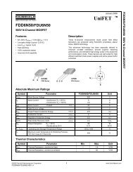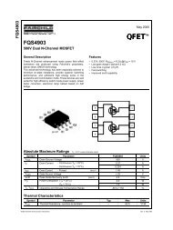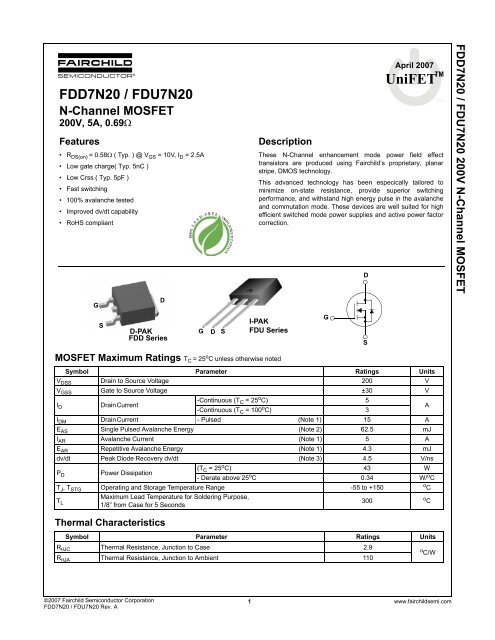
FDD7N20/FDU7N20 N-Channel MOSFET
FDD7N20/FDU7N20 N-Channel MOSFET
FDD7N20/FDU7N20 N-Channel MOSFET

Create successful ePaper yourself
Turn your PDF publications into a flip-book with our unique Google optimized e-Paper software.
<strong>FDD7N20</strong> / <strong>FDU7N20</strong><br />
N-<strong>Channel</strong> <strong>MOSFET</strong><br />
200V, 5A, 0.69Ω<br />
Features<br />
• R DS(on) = 0.58Ω ( Typ. ) @ V GS = 10V, I D = 2.5A<br />
• Low gate charge( Typ. 5nC )<br />
• Low Crss ( Typ. 5pF )<br />
• Fast switching<br />
• 100% avalanche tested<br />
• Improved dv/dt capability<br />
• RoHS compliant<br />
G<br />
S<br />
D<br />
D-PAK<br />
FDD Series<br />
G D S<br />
Description<br />
April 2007<br />
UniFET TM<br />
tm<br />
These N-<strong>Channel</strong> enhancement mode power field effect<br />
transistors are produced using Fairchild’s proprietary, planar<br />
stripe, DMOS technology.<br />
This advanced technology has been especically tailored to<br />
minimize on-state resistance, provide superior switching<br />
performance, and withstand high energy pulse in the avalanche<br />
and commutation mode. These devices are well suited for high<br />
efficient switched mode power supplies and active power factor<br />
correction.<br />
I-PAK<br />
FDU Series<br />
G<br />
D<br />
S<br />
<strong>FDD7N20</strong> / <strong>FDU7N20</strong> 200V N-<strong>Channel</strong> <strong>MOSFET</strong><br />
<strong>MOSFET</strong> Maximum Ratings T C = 25 o C unless otherwise noted<br />
Symbol Parameter Ratings Units<br />
V DSS Drain to Source Voltage 200 V<br />
V GSS Gate to Source Voltage ±30 V<br />
I D<br />
Drain Current<br />
-Continuous (T C = 25 o C) 5<br />
-Continuous (T C = 100 o C) 3<br />
A<br />
I DM Drain Current - Pulsed (Note 1) 15 A<br />
E AS Single Pulsed Avalanche Energy (Note 2) 62.5 mJ<br />
I AR Avalanche Current (Note 1) 5 A<br />
E AR Repetitive Avalanche Energy (Note 1) 4.3 mJ<br />
dv/dt Peak Diode Recovery dv/dt (Note 3) 4.5 V/ns<br />
P D<br />
Power Dissipation<br />
(T C = 25 o C) 43 W<br />
- Derate above 25 o C 0.34 W/ o C<br />
T J , T STG Operating and Storage Temperature Range -55 to +150 o C<br />
T L<br />
Maximum Lead Temperature for Soldering Purpose,<br />
1/8” from Case for 5 Seconds<br />
300 o C<br />
Thermal Characteristics<br />
Symbol Parameter Ratings Units<br />
R θJC Thermal Resistance, Junction to Case 2.9<br />
o C/W<br />
R θJA Thermal Resistance, Junction to Ambient 110<br />
©2007 Fairchild Semiconductor Corporation<br />
<strong>FDD7N20</strong> / <strong>FDU7N20</strong> Rev. A<br />
1<br />
www.fairchildsemi.com
Package Marking and Ordering Information T C = 25 o C unless otherwise noted<br />
Device Marking Device Package Reel Size Tape Width Quantity<br />
<strong>FDD7N20</strong> <strong>FDD7N20</strong>TM D-PAK 380mm 16mm 2500<br />
<strong>FDD7N20</strong> <strong>FDD7N20</strong>TF D-PAK 380mm 16mm 2000<br />
<strong>FDU7N20</strong> <strong>FDU7N20</strong> I-PAK - - 70<br />
Electrical Characteristics<br />
Symbol Parameter Test Conditions Min. Typ. Max. Units<br />
Off Characteristics<br />
BV DSS Drain to Source Breakdown Voltage I D = 250μA, V GS = 0V, T J = 25 o C 200 - - V<br />
ΔBV DSS Breakdown Voltage Temperature<br />
I<br />
/ ΔT J Coefficient<br />
D = 250μA, Referenced to 25 o C - 0.2 - V/ o C<br />
V<br />
I DSS<br />
Zero Gate Voltage Drain Current<br />
DS = 200V, V GS =0V - - 1 μA<br />
V DS = 160V, T C = 125 o C - - 10 μA<br />
I GSS Gate to Body Leakage Current V GS = ±30V, V DS = 0V - - ±100 nA<br />
On Characteristics<br />
V GS(th) Gate Threshold Voltage V GS = V DS , I D = 250μA 3.0 - 5.0 V<br />
R DS(on) Static Drain to Source On Resistance V GS = 10V, I D = 2.5A - 0.58 0.69 Ω<br />
g FS Forward Transconductance V DS = 40V, I D = 2.5A (Note 4) - 6.2 - S<br />
Dynamic Characteristics<br />
C iss<br />
Input Capacitance<br />
- 185 250 pF<br />
V DS = 25V, V GS = 0V<br />
C oss Output Capacitance - 45 65 pF<br />
f = 1MHz<br />
C rss Reverse Transfer Capacitance - 5 10 pF<br />
Q g<br />
Total Gate Charge at 10V<br />
- 5 6.7 nC<br />
Q gs Gate to Source Gate Charge V DS = 160V, I D = 7A<br />
- 1.7 - nC<br />
V GS = 10V<br />
Q gd Gate to Drain “Miller” Charge (Note 4, 5) - 2.4 - nC<br />
<strong>FDD7N20</strong> / <strong>FDU7N20</strong> 200V N-<strong>Channel</strong> <strong>MOSFET</strong><br />
Switching Characteristics<br />
t d(on) Turn-On Delay Time<br />
- 9 28 ns<br />
t r Turn-On Rise Time V DD = 100V, I D = 7A<br />
- 30 70 ns<br />
t d(off) Turn-Off Delay Time<br />
R G = 25Ω<br />
- 13 36 ns<br />
t f Turn-Off Fall Time (Note 4, 5) - 10 30 ns<br />
Drain-Source Diode Characteristics<br />
I S Maximum Continuous Drain to Source Diode Forward Current - - 5 A<br />
I SM Maximum Pulsed Drain to Source Diode Forward Current - - 20 A<br />
V SD Drain to Source Diode Forward Voltage V GS = 0V, I SD = 5A - - 1.4 V<br />
t rr Reverse Recovery Time V GS = 0V, I SD = 7A<br />
- 120 - ns<br />
Q rr Reverse Recovery Charge dI F /dt = 100A/μs (Note 4) - 0.4 - μC<br />
Notes:<br />
1. Repetitive Rating: Pulse width limited by maximum junction temperature<br />
2. L =5mH, I AS = 5A, V DD = 50V, R G = 25Ω, Starting T J = 25°C<br />
3. I SD ≤ 5A, di/dt ≤ 200A/μs, V DD ≤ BV DSS , Starting T J = 25°C<br />
4. Pulse Test: Pulse width ≤ 300μs, Duty Cycle ≤ 2%<br />
5. Essentially Independent of Operating Temperature Typical Characteristics<br />
<strong>FDD7N20</strong> / <strong>FDU7N20</strong> Rev. A<br />
2<br />
www.fairchildsemi.com
Typical Performance Characteristics<br />
ID,Drain Current[A]<br />
Figure 1. On-Region Characteristics<br />
20<br />
10<br />
1<br />
0.1<br />
V GS = 10.0 V<br />
8.0 V<br />
7.0 V<br />
6.5 V<br />
6.0 V<br />
5.5 V<br />
Figure 2. Transfer Characteristics<br />
* Notes :<br />
* Notes :<br />
1. 250μs Pulse Test<br />
2. T C = 25 o 1. V DS = 25V<br />
C<br />
2. 250μs Pulse Test<br />
0.01<br />
1<br />
0.04 0.1 1 10 25<br />
4 6 8 10 12<br />
V DS ,Drain-Source Voltage[V]<br />
V GS ,Gate-Source Voltage[V]<br />
Figure 3. On-Resistance Variation vs.<br />
Figure 4. Body Diode Forward Voltage<br />
Drain Current and Gate Voltage Variation vs. Source Current<br />
and Temperature<br />
1.5<br />
ID,Drain Current[A]<br />
20<br />
10<br />
200<br />
100<br />
25 o C<br />
150 o C<br />
-55 o C<br />
<strong>FDD7N20</strong> / <strong>FDU7N20</strong> 200V N-<strong>Channel</strong> <strong>MOSFET</strong><br />
RDS(ON) [Ω],<br />
Drain-Source On-Resistance<br />
1.2<br />
0.9<br />
0.6<br />
V GS = 10V<br />
V GS = 20V<br />
* Note : T J = 25 o C<br />
0.3<br />
0 2 4 6 8 10<br />
I D , Drain Current [A]<br />
IS, Reverse Drain Current [A]<br />
10<br />
1<br />
150 o C<br />
25 o C<br />
Notes:<br />
1. V GS<br />
= 0V<br />
2. 250μs Pulse Test<br />
0.2<br />
0.0 0.7 1.4 2.1 2.8 3.5<br />
V SD<br />
, Body Diode Forward Voltage [V]<br />
Capacitances [pF]<br />
Figure 5. Capacitance Characteristics<br />
500<br />
400<br />
300<br />
200<br />
100<br />
C oss<br />
C iss<br />
C rss<br />
Ciss = Cgs + Cgd (Cds = shorted)<br />
Coss = Cds + Cgd<br />
Crss = Cgd<br />
* Note:<br />
1. V GS = 0V<br />
2. f = 1MHz<br />
Figure 6. Gate Charge Characteristics<br />
VGS, Gate-Source Voltage [V]<br />
10<br />
8<br />
V DS = 160V<br />
6<br />
V DS = 100V<br />
V DS = 50V<br />
4<br />
2<br />
0<br />
0.1 1 10<br />
V DS , Drain-Source Voltage [V]<br />
* Note : I D = 7A<br />
0<br />
30 0 1 2 3 4 5 6<br />
Q g , Total Gate Charge [nC]<br />
<strong>FDD7N20</strong> / <strong>FDU7N20</strong> Rev. A<br />
3<br />
www.fairchildsemi.com
Typical Performance Characteristics (Continued)<br />
BVDSS, [Normalized]<br />
Drain-Source Breakdown Voltage<br />
ID, Drain Current [A]<br />
Figure 7. Breakdown Voltage Variation<br />
vs. Temperature<br />
1.2<br />
1.1<br />
1.0<br />
0.9<br />
* Notes :<br />
1. V GS = 0V<br />
2. I D = 250μA<br />
0.8<br />
-100 -50 0 50 100 150 200<br />
T J , Junction Temperature [ o C]<br />
Figure 9. Maximum Safe Operating Area<br />
50<br />
10<br />
1<br />
0.1<br />
Operation in This Area<br />
is Limited by R DS(on)<br />
* Notes :<br />
1. T C = 25 o C<br />
2. T J = 150 o C<br />
3. Single Pulse<br />
0.01<br />
1 10 100<br />
V DS , Drain-Source Voltage [V]<br />
20μs<br />
100μs<br />
1ms<br />
10ms<br />
DC<br />
500<br />
RDS(on), [Normalized]<br />
Drain-Source On-Resistance<br />
Figure 8. On-Resistance Variation<br />
vs. Temperature<br />
3.0<br />
2.5<br />
2.0<br />
1.5<br />
1.0<br />
0.5<br />
* Notes :<br />
1. V GS = 10V<br />
2. I D = 2.5A<br />
0.0<br />
-100 -50 0 50 100 150 200<br />
T J , Junction Temperature [ o C]<br />
Figure 10. Maximum Drain Current<br />
vs. Case Temperature<br />
ID, Drain Current [A]<br />
6<br />
5<br />
4<br />
3<br />
2<br />
1<br />
0<br />
25 50 75 100 125 150<br />
T C , Case Temperature [ o C]<br />
<strong>FDD7N20</strong> / <strong>FDU7N20</strong> 200V N-<strong>Channel</strong> <strong>MOSFET</strong><br />
Figure 11. Transient Thermal Response Curve<br />
5<br />
Thermal Response [Z θJC ]<br />
1<br />
0.1<br />
0.5<br />
0.2<br />
0.1<br />
0.05<br />
0.02<br />
0.01<br />
P DM<br />
t 1<br />
t 2<br />
* Notes :<br />
1. Z θJC (t) = 2.9 o C/W Max.<br />
Single pulse<br />
2. Duty Factor, D=t 1 /t 2<br />
3. T JM - T C = P DM * Z θJC (t)<br />
0.01<br />
10 -5 10 -4 10 -3 10 -2 10 -1 10 0 10 1<br />
Rectangular Pulse Duration [sec]<br />
<strong>FDD7N20</strong> / <strong>FDU7N20</strong> Rev. A<br />
4<br />
www.fairchildsemi.com
Gate Charge Test Circuit & Waveform<br />
Resistive Switching Test Circuit & Waveforms<br />
<strong>FDD7N20</strong> / <strong>FDU7N20</strong> 200V N-<strong>Channel</strong> <strong>MOSFET</strong><br />
Unclamped Inductive Switching Test Circuit & Waveforms<br />
<strong>FDD7N20</strong> / <strong>FDU7N20</strong> Rev. A<br />
5<br />
www.fairchildsemi.com
Peak Diode Recovery dv/dt Test Circuit & Waveforms<br />
D U T<br />
+<br />
I S D<br />
V D<br />
S<br />
_<br />
L<br />
D<br />
r iv e r<br />
R G S a m e T y p e<br />
a s D U<br />
T<br />
V G S • d v / d t c o n t r o lle d b y R G<br />
• I S D c o n t r o lle d b y p u ls e p e r io d<br />
V D<br />
D<br />
<strong>FDD7N20</strong> / <strong>FDU7N20</strong> 200V N-<strong>Channel</strong> <strong>MOSFET</strong><br />
V G<br />
S<br />
( D riv e r )<br />
G a t e P u ls e W id t h<br />
D =<br />
--------------------------<br />
G<br />
a t e P u ls e P e r io d<br />
1 0 V<br />
I F M , B o d y D io d e F o r w a r d C u r r e n t<br />
I S D<br />
( D U T )<br />
d i/ d t<br />
I R<br />
M<br />
B o d y D io d e R e v e r s e C u r r e n t<br />
V D<br />
S<br />
( D U T )<br />
B o d y D io d e R e c o v e r y d v / d t<br />
V S D<br />
V D<br />
D<br />
B o d y D<br />
io d e<br />
F o r w a r d V o lt a g e D r o p<br />
<strong>FDD7N20</strong> / <strong>FDU7N20</strong> Rev. A<br />
6<br />
www.fairchildsemi.com
Mechanical Dimensions<br />
D-PAK<br />
<strong>FDD7N20</strong> / <strong>FDU7N20</strong> 200V N-<strong>Channel</strong> <strong>MOSFET</strong><br />
<strong>FDD7N20</strong> / <strong>FDU7N20</strong> Rev. A<br />
7<br />
www.fairchildsemi.com
Mechanical Dimensions<br />
I-PAK<br />
<strong>FDD7N20</strong> / <strong>FDU7N20</strong> 200V N-<strong>Channel</strong> <strong>MOSFET</strong><br />
<strong>FDD7N20</strong> / <strong>FDU7N20</strong> Rev. A<br />
8<br />
www.fairchildsemi.com
TRADEMARKS<br />
The following are registered and unregistered trademarks and service marks Fairchild Semiconductor owns or is authorized to use and is not<br />
intended to be an exhaustive list of all such trademarks.<br />
ACEx ®<br />
Build it Now<br />
CorePLUS<br />
CROSSVOLT<br />
CTL<br />
Current Transfer Logic<br />
EcoSPARK ®<br />
FACT Quiet Series<br />
FACT ®<br />
FAST ®<br />
FastvCore<br />
FPS<br />
FRFET ®<br />
Global Power Resource SM<br />
Green FPS<br />
Green FPS e-Series<br />
GTO<br />
i-Lo<br />
IntelliMAX<br />
ISOPLANAR<br />
MegaBuck<br />
MICROCOUPLER<br />
MicroPak<br />
Motion-SPM<br />
OPTOLOGIC ®<br />
OPTOPLANAR ®<br />
PDP-SPM<br />
Power220 ®<br />
Power247 ®<br />
POWEREDGE ®<br />
Power-SPM<br />
PowerTrench ®<br />
Programmable Active Droop<br />
QFET ®<br />
QS<br />
QT Optoelectronics<br />
Quiet Series<br />
RapidConfigure<br />
SMART START<br />
SPM ®<br />
STEALTH<br />
SuperFET<br />
SuperSOT-3<br />
SuperSOT-6<br />
SuperSOT-8<br />
SyncFET<br />
The Power Franchise ®<br />
<br />
TinyBoost<br />
TinyBuck<br />
TinyLogic ®<br />
TINYOPTO<br />
TinyPower<br />
TinyPWM<br />
TinyWire<br />
μSerDes<br />
UHC ®<br />
UniFET<br />
VCX<br />
DISCLAIMER<br />
FAIRCHILD SEMICONDUCTOR RESERVES THE RIGHT TO MAKE CHANGES WITHOUT FURTHER NOTICE TO ANY PRODUCTS<br />
HEREIN TO IMPROVE RELIABILITY, FUNCTION, OR DESIGN. FAIRCHILD DOES NOT ASSUME ANY LIABILITY ARISING OUT OF THE<br />
APPLICATION OR USE OF ANY PRODUCT OR CIRCUIT DESCRIBED HEREIN; NEITHER DOES IT CONVEY ANY LICENSE UNDER ITS<br />
PATENT RIGHTS, NOR THE RIGHTS OF OTHERS. THESE SPECIFICATIONS DO NOT EXPAND THE TERMS OF FAIRCHILD’S<br />
WORLDWIDE TERMS AND CONDITIONS, SPECIFICALLY THE WARRANTY THEREIN, WHICH COVERS THESE PRODUCTS.<br />
LIFE SUPPORT POLICY<br />
FAIRCHILD’S PRODUCTS ARE NOT AUTHORIZED FOR USE AS CRITICAL COMPONENTS IN LIFE SUPPORT DEVICES OR<br />
SYSTEMS WITHOUT THE EXPRESS WRITTEN APPROVAL OF FAIRCHILD SEMICONDUCTOR CORPORATION.<br />
As used herein:<br />
1. Life support devices or systems are devices or systems<br />
which, (a) are intended for surgical implant into the body or<br />
(b) support or sustain life, and (c) whose failure to perform<br />
when properly used in accordance with instructions for use<br />
provided in the labeling, can be reasonably expected to<br />
result in a significant injury of the user.<br />
2. A critical component in any component of a life support,<br />
device, or system whose failure to perform can be<br />
reasonably expected to cause the failure of the life support<br />
device or system, or to affect its safety or effectiveness.<br />
PRODUCT STATUS DEFINITIONS<br />
Definition of Terms<br />
Datasheet Identification Product Status Definition<br />
Advance Information Formative or In Design This datasheet contains the design specifications for product<br />
development. Specifications may change in any manner without notice.<br />
Preliminary First Production This datasheet contains preliminary data; supplementary data will be<br />
published at a later date. Fairchild Semiconductor reserves the right to<br />
make changes at any time without notice to improve design.<br />
No Identification Needed Full Production This datasheet contains final specifications. Fairchild Semiconductor<br />
reserves the right to make changes at any time without notice to improve<br />
design.<br />
Obsolete Not In Production This datasheet contains specifications on a product that has been<br />
discontinued by Fairchild Semiconductor. The datasheet is printed for<br />
reference information only.<br />
Rev. I28<br />
© 2007 Fairchild Semiconductor Corporation www.fairchildsemi.com