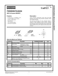
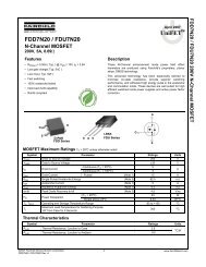
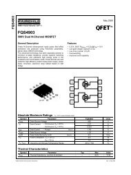
FDD6682/FDU6682 30V N-Channel PowerTrench® MOSFET
FDD6682/FDU6682 30V N-Channel PowerTrench® MOSFET
FDD6682/FDU6682 30V N-Channel PowerTrench® MOSFET

Create successful ePaper yourself
Turn your PDF publications into a flip-book with our unique Google optimized e-Paper software.
<strong>FDD6682</strong>/<strong>FDU6682</strong><br />
<strong>30V</strong> N-<strong>Channel</strong> PowerTrench <strong>MOSFET</strong><br />
General Description<br />
Features<br />
June 2004<br />
<strong>FDD6682</strong>/<strong>FDU6682</strong><br />
This N-<strong>Channel</strong> <strong>MOSFET</strong> has been designed<br />
specifically to improve the overall efficiency of DC/DC<br />
converters using either synchronous or conventional<br />
switching PWM controllers. It has been optimized for<br />
low gate charge, low RDS( ON) and fast switching speed.<br />
Applications<br />
• DC/DC converter<br />
• Motor Drives<br />
• 75 A, 30 V R DS(ON) = 6.2 mΩ @ V GS = 10 V<br />
R DS(ON) = 8.0 mΩ @ V GS = 4.5 V<br />
• Low gate charge<br />
• Fast switching<br />
• High performance trench technology for extremely<br />
low R DS(ON)<br />
D<br />
G<br />
D<br />
S<br />
D-PAK TO-252<br />
(TO-252)<br />
G D S<br />
I-PAK<br />
(TO-251AA)<br />
G<br />
S<br />
Absolute Maximum Ratings<br />
TA=25 o C unless otherwise noted<br />
P D<br />
Symbol Parameter Ratings Units<br />
V DSS Drain-Source Voltage 30 V<br />
V GSS Gate-Source Voltage ±20<br />
I D Drain Current – Continuous (Note 3) 75 A<br />
– Pulsed (Note 1a) 100<br />
Power Dissipation for Single Operation (Note 1) 71<br />
W<br />
(Note 1a) 3.8<br />
(Note 1b) 1.6<br />
T J, T STG Operating and Storage Junction Temperature Range –55 to +175 °C<br />
Thermal Characteristics<br />
R θJC Thermal Resistance, Junction-to-Case (Note 1) 2.1 °C/W<br />
R θJA Thermal Resistance, Junction-to-Ambient (Note 1a) 40<br />
R θJA Thermal Resistance, Junction-to-Ambient (Note 1b) 96<br />
Package Marking and Ordering Information<br />
Device Marking Device Package Reel Size Tape width Quantity<br />
<strong>FDD6682</strong> <strong>FDD6682</strong> D-PAK (TO-252) 13’’ 12mm 2500 units<br />
<strong>FDU6682</strong> <strong>FDU6682</strong> I-PAK (TO-251) Tube N/A 75<br />
©2004 Fairchild Semiconductor Corporation <strong>FDD6682</strong>/<strong>FDU6682</strong> Rev H(W)
Electrical Characteristics<br />
T A<br />
= 25°C unless otherwise noted<br />
Symbol Parameter Test Conditions Min Typ Max Units<br />
Drain-Source Avalanche Ratings (Note 2)<br />
W DSS Drain-Source Avalanche Energy Single Pulse, V DD = 15 V, I D = 17 A 240 mJ<br />
I AR Drain-Source Avalanche Current 17 A<br />
Off Characteristics<br />
BV DSS Drain–Source Breakdown Voltage V GS = 0 V, I D = 250 µA 30 V<br />
∆BVDSS Breakdown Voltage Temperature I D = 250 µA, Referenced to 25°C 20 mV/°C<br />
∆T J Coefficient<br />
I DSS Zero Gate Voltage Drain Current V DS = 24 V, V GS = 0 V 1 µA<br />
I GSS Gate–Body Leakage V GS = ±20 V, V DS = 0 V ±100 nA<br />
<strong>FDD6682</strong>/<strong>FDU6682</strong><br />
On Characteristics (Note 2)<br />
V GS(th) Gate Threshold Voltage V DS = V GS, I D = 250 µA 1 1.9 3 V<br />
∆VGS(th) Gate Threshold Voltage<br />
I D = 250 µA, Referenced to 25°C –7 mV/°C<br />
∆T J<br />
Temperature Coefficient<br />
R DS(on) Static Drain–Source<br />
V GS = 10 V, I D = 17 A<br />
5.2 6.2 mΩ<br />
On–Resistance<br />
V GS = 4.5 V, I D = 15 A<br />
6.4 8<br />
V GS = 10 V, I D = 17 A, T J=125°C<br />
8.0 11.9<br />
I D(on) On–State Drain Current V GS = 10 V, V DS = 5 V 50 A<br />
g FS Forward Transconductance V DS = 5 V, I D = 17 A 65 S<br />
Dynamic Characteristics<br />
C iss Input Capacitance 2400 pF<br />
V DS = 15 V, V GS = 0 V,<br />
C oss Output Capacitance 577 pF<br />
f = 1.0 MHz<br />
C rss Reverse Transfer Capacitance<br />
258 pF<br />
R G Gate Resistance V GS = 15 mV, f = 1.0 MHz 1.4 Ω<br />
Switching Characteristics (Note 2)<br />
t d(on) Turn–On Delay Time 14 20 ns<br />
t r Turn–On Rise Time V DD = 15 V, I D = 1 A,<br />
12 37 ns<br />
t d(off) Turn–Off Delay Time V GS = 10 V, R GEN = 6 Ω<br />
38 64 ns<br />
t f<br />
Turn–Off Fall Time<br />
18 32 ns<br />
Q g Total Gate Charge 24 31 nC<br />
Q gs Gate–Source Charge<br />
V DS = 15V,<br />
V GS = 5 V<br />
I D = 17 A,<br />
6.5 nC<br />
Gate–Drain Charge<br />
8.1 nC<br />
Q gd<br />
<strong>FDD6682</strong>/<strong>FDU6682</strong> Rev H(W)
Electrical Characteristics (continued)<br />
T A<br />
= 25°C unless otherwise noted<br />
Symbol Parameter Test Conditions Min Typ Max Units<br />
Drain–Source Diode Characteristics and Maximum Ratings<br />
I S Maximum Continuous Drain–Source Diode Forward Current 3.2 A<br />
V SD Drain–Source Diode Forward V GS = 0 V, I S = 3.2 A (Note 2) 0.7 1.2 V<br />
Voltage<br />
t rr Diode Reverse Recovery Time I F = 17 A, d iF/d t = 100 A/µs 32 nS<br />
Q rr Diode Reverse Recovery Charge 20 nC<br />
<strong>FDD6682</strong>/<strong>FDU6682</strong><br />
Notes:<br />
1. R θJA<br />
is the sum of the junction-to-case and case-to-ambient thermal resistance where the case thermal reference is defined as the solder mounting surface of<br />
the drain pins. R θJC<br />
is guaranteed by design while R θCA<br />
is determined by the user's board design.<br />
a) R θJA<br />
= 40°C/W when mounted on a<br />
1in 2 pad of 2 oz copper<br />
b) R θJA<br />
= 96°C/W when mounted<br />
on a minimum pad.<br />
Scale 1 : 1 on letter size paper<br />
2. Pulse Test: Pulse Width < 300µs, Duty Cycle < 2.0%<br />
3. Maximum current is calculated as:<br />
PD<br />
R DS(ON)<br />
where PD is maximum power dissipation at TC = 25°C and RDS(on) is at TJ(max) and VGS = 10V. Package current limitation is 21A<br />
<strong>FDD6682</strong>/<strong>FDU6682</strong> Rev H(W)
Typical Characteristics<br />
I D , DRAIN CURRENT (A)<br />
100<br />
V GS =10V<br />
4.0V<br />
80<br />
6.0V<br />
4.5V<br />
60<br />
40<br />
20<br />
3.5V<br />
3.0V<br />
R DS(ON) , NORMALIZED<br />
DRAIN-SOURCE ON-RESISTANCE<br />
2<br />
1.8<br />
1.6<br />
1.4<br />
1.2<br />
1<br />
V GS = 3.5V<br />
4.0V<br />
4.5V<br />
5.0V<br />
10V<br />
<strong>FDD6682</strong>/<strong>FDU6682</strong><br />
0<br />
0 1 2 3<br />
V DS , DRAIN-SOURCE VOLTAGE (V)<br />
0.8<br />
0 20 40 60 80 100<br />
I D , DRAIN CURRENT (A)<br />
Figure 1. On-Region Characteristics.<br />
Figure 2. On-Resistance Variation with<br />
Drain Current and Gate Voltage.<br />
2<br />
0.02<br />
R DS(ON) , NORMALIZED<br />
DRAIN-SOURCE ON-RESISTANCE<br />
1.8<br />
1.6<br />
1.4<br />
1.2<br />
1<br />
0.8<br />
I D = 17A<br />
V GS = 10V<br />
R DS(ON) , ON-RESISTANCE (OHM)<br />
0.015<br />
0.01<br />
0.005<br />
T A = 25 o C<br />
T A = 125 o C<br />
I D = 8.5A<br />
0.6<br />
-50 -25 0 25 50 75 100 125 150 175<br />
T J, JUNCTION TEMPERATURE ( o C)<br />
0<br />
2 4 6 8 10<br />
V GS , GATE TO SOURCE VOLTAGE (V)<br />
Figure 3. On-Resistance Variation with<br />
Temperature.<br />
Figure 4. On-Resistance Variation with<br />
Gate-to-Source Voltage.<br />
I D , DRAIN CURRENT (A)<br />
80<br />
V DS = 5V<br />
60<br />
40<br />
20<br />
T A =125 o C<br />
25 o C<br />
-55 o C<br />
0<br />
1 2 3 4<br />
V GS , GATE TO SOURCE VOLTAGE (V)<br />
I S, REVERSE DRAIN CURRENT (A)<br />
100<br />
10<br />
1<br />
0.1<br />
0.01<br />
0.001<br />
0.0001<br />
V GS = 0V<br />
T A = 125 o C<br />
25 o C<br />
-55 o C<br />
0 0.2 0.4 0.6 0.8 1 1.2<br />
V SD, BODY DIODE FORWARD VOLTAGE (V)<br />
Figure 5. Transfer Characteristics<br />
Figure 6. Body Diode Forward Voltage Variation<br />
with Source Current and Temperature<br />
<strong>FDD6682</strong>/<strong>FDU6682</strong> Rev H(W)
Typical Characteristics<br />
V GS, GATE-SOURCE VOLTAGE (V)<br />
10<br />
V<br />
I D = 17A<br />
DS = 10V<br />
8<br />
20V<br />
6<br />
4<br />
2<br />
15V<br />
CAPACITANCE (pF)<br />
3500<br />
3000<br />
2500<br />
2000<br />
1500<br />
1000<br />
500<br />
C ISS<br />
C OSS<br />
C RSS<br />
f = 1MHz<br />
V GS = 0 V<br />
<strong>FDD6682</strong>/<strong>FDU6682</strong><br />
0<br />
0 10 20 30 40 50<br />
Q g , GATE CHARGE (nC)<br />
0<br />
0 5 10 15 20 25 30<br />
V DS, DRAIN TO SOURCE VOLTAGE (V)<br />
Figure 7. Gate Charge Characteristics<br />
Figure 8. Capacitance Characteristics<br />
1000<br />
100<br />
I D , DRAIN CURRENT (A)<br />
100<br />
10<br />
1<br />
0.1<br />
R DS(ON) LIMIT<br />
V GS = 10V<br />
SINGLE PULSE<br />
R θJA = 96 o C/W<br />
T A = 25 o C<br />
10s<br />
DC<br />
100ms<br />
1s<br />
1ms<br />
10ms<br />
100µs<br />
P(pk), PEAK TRANSIENT POWER (W)<br />
80<br />
60<br />
40<br />
20<br />
SINGLE PULSE<br />
R θJA = 96°C/W<br />
T A = 25°C<br />
0.01<br />
0.01 0.1 1 10 100<br />
V DS , DRAIN-SOURCE VOLTAGE (V)<br />
0<br />
0.01 0.1 1 10 100 1000<br />
t 1 , TIME (sec)<br />
Figure 9. Maximum Safe Operating Area<br />
Figure 10. Single Pulse Maximum<br />
Power Dissipation<br />
1<br />
r(t), NORMALIZED EFFECTIVE TRANSIENT<br />
THERMAL RESISTANCE<br />
0.1<br />
0.01<br />
D = 0.5<br />
0.2<br />
0.1<br />
0.05<br />
0.02<br />
0.01<br />
SINGLE PULSE<br />
0.001<br />
0.001 0.01 0.1 1 10 100 1000<br />
t 1, TIME (sec)<br />
R θJA (t) = r(t) * R θJA<br />
R θJA = 96 °C/W<br />
P(pk)<br />
t 1<br />
t 2<br />
T J - T A = P * R θJA (t)<br />
Duty Cycle, D = t 1 / t 2<br />
Figure 11. Transient Thermal Response Curve<br />
Thermal characterization performed using the conditions described in Note 1b.<br />
Transient thermal response will change depending on the circuit board design.<br />
<strong>FDD6682</strong>/<strong>FDU6682</strong> Rev H(W)
TRADEMARKS<br />
The following are registered and unregistered trademarks Fairchild Semiconductor owns or is authorized to use and is<br />
not intended to be an exhaustive list of all such trademarks.<br />
ACEx<br />
ActiveArray<br />
Bottomless<br />
CoolFET<br />
CROSSVOLT<br />
DOME<br />
EcoSPARK<br />
E 2 CMOS<br />
EnSigna<br />
FACT<br />
FACT Quiet Series<br />
DISCLAIMER<br />
FAIRCHILD SEMICONDUCTOR RESERVES THE RIGHT TO MAKE CHANGES WITHOUT FURTHER NOTICE TO ANY<br />
PRODUCTS HEREIN TO IMPROVE RELIABILITY, FUNCTION OR DESIGN. FAIRCHILD DOES NOT ASSUME ANY LIABILITY<br />
ARISING OUT OF THE APPLICATION OR USE OF ANY PRODUCT OR CIRCUIT DESCRIBED HEREIN; NEITHER DOES IT<br />
CONVEY ANY LICENSE UNDER ITS PATENT RIGHTS, NOR THE RIGHTS OF OTHERS.<br />
LIFE SUPPORT POLICY<br />
FAIRCHILD’S PRODUCTS ARE NOT AUTHORIZED FOR USE AS CRITICAL COMPONENTS IN LIFE SUPPORT<br />
DEVICES OR SYSTEMS WITHOUT THE EXPRESS WRITTEN APPROVAL OF FAIRCHILD SEMICONDUCTOR CORPORATION.<br />
As used herein:<br />
1. Life support devices or systems are devices or<br />
systems which, (a) are intended for surgical implant into<br />
the body, or (b) support or sustain life, or (c) whose<br />
failure to perform when properly used in accordance<br />
with instructions for use provided in the labeling, can be<br />
reasonably expected to result in significant injury to the<br />
user.<br />
PRODUCT STATUS DEFINITIONS<br />
Definition of Terms<br />
FAST ®<br />
FASTr<br />
FPS<br />
FRFET<br />
GlobalOptoisolator<br />
GTO<br />
HiSeC<br />
I 2 C<br />
i-Lo<br />
ImpliedDisconnect<br />
Across the board. Around the world.<br />
The Power Franchise ®<br />
Programmable Active Droop<br />
ISOPLANAR<br />
LittleFET<br />
MICROCOUPLER<br />
MicroFET<br />
MicroPak<br />
MICROWIRE<br />
MSX<br />
MSXPro<br />
OCX<br />
OCXPro<br />
OPTOLOGIC ®<br />
OPTOPLANAR<br />
PACMAN<br />
POP<br />
Power247<br />
PowerSaver<br />
PowerTrench ®<br />
QFET ®<br />
QS<br />
QT Optoelectronics<br />
Quiet Series<br />
RapidConfigure<br />
RapidConnect<br />
µSerDes<br />
SILENT SWITCHER ®<br />
SMART START<br />
SPM<br />
Stealth<br />
2. A critical component is any component of a life<br />
support device or system whose failure to perform can<br />
be reasonably expected to cause the failure of the life<br />
support device or system, or to affect its safety or<br />
effectiveness.<br />
Datasheet Identification Product Status Definition<br />
SuperFET<br />
SuperSOT-3<br />
SuperSOT-6<br />
SuperSOT-8<br />
SyncFET<br />
TinyLogic ®<br />
TINYOPTO<br />
TruTranslation<br />
UHC<br />
UltraFET ®<br />
VCX<br />
Advance Information<br />
Preliminary<br />
No Identification Needed<br />
Formative or<br />
In Design<br />
First Production<br />
Full Production<br />
This datasheet contains the design specifications for<br />
product development. Specifications may change in<br />
any manner without notice.<br />
This datasheet contains preliminary data, and<br />
supplementary data will be published at a later date.<br />
Fairchild Semiconductor reserves the right to make<br />
changes at any time without notice in order to improve<br />
design.<br />
This datasheet contains final specifications. Fairchild<br />
Semiconductor reserves the right to make changes at<br />
any time without notice in order to improve design.<br />
Obsolete<br />
Not In Production<br />
This datasheet contains specifications on a product<br />
that has been discontinued by Fairchild semiconductor.<br />
The datasheet is printed for reference information only.<br />
Rev. I11