FAN7380 Half-Bridge Gate Driver - Fairchild Semiconductor
FAN7380 Half-Bridge Gate Driver - Fairchild Semiconductor
FAN7380 Half-Bridge Gate Driver - Fairchild Semiconductor

Create successful ePaper yourself
Turn your PDF publications into a flip-book with our unique Google optimized e-Paper software.
<strong>FAN7380</strong><br />
<strong>Half</strong>-<strong>Bridge</strong> <strong>Gate</strong> <strong>Driver</strong><br />
Features<br />
• Floating Channel Designed for Bootstrapping<br />
Operation to +600V<br />
• Typically 90mA/180mA Sourcing/Sinking Current<br />
Driving Capability for Both Channels<br />
• Common-Mode dv/dt Noise Canceling Circuit<br />
• Extended Allowable Negative V S Swing to -9.8V for<br />
Signal Propagation at V CC =V BS =15V<br />
• V CC & V BS Supply Range from 10V to 20V<br />
• UVLO Functions for Both Channels<br />
• TTL-Compatible Input Logic Threshold Levels<br />
• Matched Propagation Delay Below 50ns<br />
• Built-in 100ns Dead-Time Control Function<br />
• Output in Phase with Input Signal<br />
Typical Applications<br />
• Fluorescent Lamp Ballast<br />
• Compact Fluorescent Lamp Ballast<br />
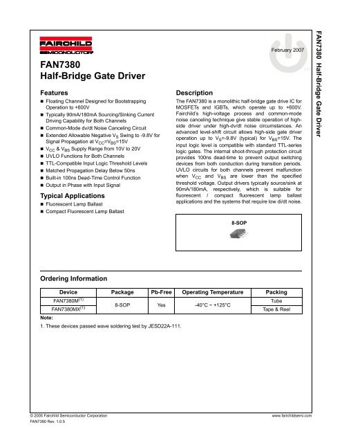
Description<br />
February 2007<br />
The <strong>FAN7380</strong> is a monolithic half-bridge gate drive IC for<br />
MOSFETs and IGBTs, which operate up to +600V.<br />
<strong>Fairchild</strong>’s high-voltage process and common-mode<br />
noise canceling technique give stable operation of highside<br />
driver under high-dv/dt noise circumstances. An<br />
advanced level-shift circuit allows high-side gate driver<br />
operation up to V S =-9.8V (typical) for V BS =15V. The<br />
input logic level is compatible with standard TTL-series<br />
logic gates. The internal shoot-through protection circuit<br />
provides 100ns dead-time to prevent output switching<br />
devices from both conduction during transition periods.<br />
UVLO circuits for both channels prevent malfunction<br />
when V CC and V BS are lower than the specified<br />
threshold voltage. Output drivers typically source/sink at<br />
90mA/180mA, respectively, which is suitable for<br />
fluorescent / compact fluorescent lamp ballast<br />
applications and the systems that require low di/dt noise.<br />
<strong>FAN7380</strong> <strong>Half</strong>-<strong>Bridge</strong> <strong>Gate</strong> <strong>Driver</strong><br />
8-SOP<br />
Ordering Information<br />
Device Package Pb-Free Operating Temperature Packing<br />
<strong>FAN7380</strong>M (1) Tube<br />
8-SOP Yes -40°C ~ +125°C<br />
<strong>FAN7380</strong>MX (1)<br />
Tape & Reel<br />
Note:<br />
1. These devices passed wave soldering test by JESD22A-111.<br />
© 2005 <strong>Fairchild</strong> <strong>Semiconductor</strong> Corporation www.fairchildsemi.com<br />
<strong>FAN7380</strong> Rev. 1.0.5
Typical Application Circuit<br />
15V<br />
LIN<br />
1 LIN<br />
R BOOT D BOOT<br />
V B<br />
HIN<br />
2 HIN HO 7<br />
V S<br />
3 V CC 6<br />
C1<br />
4 COM LO 5<br />
8<br />
C BOOT<br />
R1<br />
R3<br />
R2<br />
Q1<br />
Q2<br />
600V<br />
Load<br />
<strong>FAN7380</strong> <strong>Half</strong>-<strong>Bridge</strong> <strong>Gate</strong> <strong>Driver</strong><br />
R4<br />
<strong>FAN7380</strong> Rev.03<br />
Figure 1. Application Circuit for Fluorescent Lamp Ballast<br />
Internal Block Diagram<br />
8<br />
V B<br />
UVLO<br />
HIN<br />
2<br />
SCHMITT TRIGGER<br />
INPUT<br />
HS(ON/OFF)<br />
PULSE<br />
GENERATOR<br />
NOISE<br />
CANCELLER<br />
R<br />
R<br />
S<br />
Q<br />
DRIVER<br />
7<br />
6<br />
HO<br />
V S<br />
UVLO<br />
3<br />
V CC<br />
LIN<br />
1<br />
SHOOT THOUGH<br />
PREVENTION<br />
{DEAD-TIME=100ns}<br />
LS(ON/OFF)<br />
DELAY<br />
DRIVER<br />
5<br />
LO<br />
4<br />
COM<br />
<strong>FAN7380</strong> Rev.02<br />
Figure 2. Functional Block Diagram of <strong>FAN7380</strong><br />
© 2005 <strong>Fairchild</strong> <strong>Semiconductor</strong> Corporation www.fairchildsemi.com<br />
<strong>FAN7380</strong> Rev. 1.0.5 2
Pin Configuration<br />
LIN<br />
HIN<br />
V CC<br />
COM<br />
1<br />
2<br />
3<br />
4<br />
<strong>FAN7380</strong><br />
8<br />
7<br />
6<br />
5<br />
<strong>FAN7380</strong> Rev.02<br />
V B<br />
HO<br />
V S<br />
LO<br />
<strong>FAN7380</strong> <strong>Half</strong>-<strong>Bridge</strong> <strong>Gate</strong> <strong>Driver</strong><br />
Figure 3. Pin Configuration (Top View)<br />
Pin Definitions<br />
Pin # Name I/O Description<br />
1 LIN I Logic Input for Low-Side <strong>Gate</strong> <strong>Driver</strong> Output<br />
2 HIN I Logic Input for High-Side <strong>Gate</strong> <strong>Driver</strong> Output<br />
3 V CC I Low-Side Supply Voltage<br />
4 COM Logic Ground and Low-Side <strong>Driver</strong> Return<br />
5 LO O Low-Side <strong>Driver</strong> Output<br />
6 V S I High-Voltage Floating Supply Return<br />
7 HO O High-Side <strong>Driver</strong> Output<br />
8 V B I High-Side Floating Supply<br />
© 2005 <strong>Fairchild</strong> <strong>Semiconductor</strong> Corporation www.fairchildsemi.com<br />
<strong>FAN7380</strong> Rev. 1.0.5 3
Absolute Maximum Ratings<br />
Stresses exceeding the absolute maximum ratings may damage the device. The device may not function or be<br />
operable above the recommended operating conditions and stressing the parts to these levels is not recommended. In<br />
addition, extended exposure to stresses above the recommended operating conditions may affect device reliability.<br />
The absolute maximum ratings are stress ratings only. T A =25°C, unless otherwise specified.<br />
Symbol Parameter Min. Max. Unit<br />
V S High-side offset voltage V B -25 V B +0.3<br />
V B High-side floating supply voltage -0.3 625<br />
V HO High-side floating output voltage HO V S -0.3 V B +0.3<br />
V CC Low-side and logic-fixed supply voltage -0.3 25<br />
V<br />
V LO Low-side output voltage LO -0.3 V CC +0.3<br />
V IN Logic input voltage (HIN, LIN) -0.3 V CC +0.3<br />
COM Logic ground V CC -25 V CC +0.3<br />
dV S /dt Allowable offset voltage slew rate 50 V/ns<br />
(2)(3)(4)<br />
P D Power dissipation 0.625 W<br />
θ JA Thermal resistance, junction-to-ambient 200 °C/W<br />
T J Junction temperature 150 °C<br />
T S Storage temperature -50 150 °C<br />
<strong>FAN7380</strong> <strong>Half</strong>-<strong>Bridge</strong> <strong>Gate</strong> <strong>Driver</strong><br />
Notes:<br />
2. Mounted on 76.2 x 114.3 x 1.6mm PCB (FR-4 glass epoxy material).<br />
3. Refer to the following standards:<br />
JESD51-2: Integral circuits thermal test method environmental conditions - natural convection<br />
JESD51-3: Low effective thermal conductivity test board for leaded surface mount packages<br />
4. Do not exceed P D under any circumstances.<br />
Recommended Operating Ratings<br />
The Recommended Operating Conditions table defines the conditions for actual device operation. Recommended<br />
operating conditions are specified to ensure optimal performance to the datasheet specifications. <strong>Fairchild</strong> does not<br />
recommend exceeding them or designing to Absolute Maximum Ratings.<br />
Symbol Parameter Min. Max. Unit<br />
V B High-side floating supply voltage V S +10 V S +20<br />
V S High-side floating supply offset voltage 6-V CC 600<br />
V HO High-side (HO) output voltage V S V B<br />
V LO Low-side (LO) output voltage COM V CC<br />
V<br />
V IN Logic input voltage (HIN, LIN) COM V CC<br />
V CC Low-side supply voltage 10 20<br />
T A Ambient temperature -40 125 °C<br />
© 2005 <strong>Fairchild</strong> <strong>Semiconductor</strong> Corporation www.fairchildsemi.com<br />
<strong>FAN7380</strong> Rev. 1.0.5 4
Static Electrical Characteristics<br />
V BIAS (V CC , V BS ) = 15.0V, T A = 25°C, unless otherwise specified. The V IN and I IN parameters are referenced to COM.<br />
The V O and I O parameters are referenced to V S and COM and are applicable to the respective outputs HO and LO.<br />
Symbol Parameter Conditions Min. Typ. Max. Unit<br />
V CCUV +<br />
V BSUV +<br />
V CCUV -<br />
V BSUV -<br />
V CCUVH<br />
V BSUVH<br />
V CC & V BS supply under-voltage<br />
positive going threshold<br />
V CC & V BS supply under-voltage<br />
negative going threshold<br />
V CC supply under-voltage lockout<br />
hysteresis<br />
8.2 9.2 10.0<br />
7.6 8.7 9.6<br />
I LK Offset supply leakage current V B =V S =600V 50<br />
I QBS Quiescent V BS supply current V IN =0V or 5V 44 100 µA<br />
I QCC Quiescent V CC supply current V IN =0V or 5V 70 180<br />
I PBS Operating V BS supply current f IN =20kHz, rms value 600<br />
I PCC Operating V CC supply current f IN =20kHz, rms value 610<br />
µA<br />
V IH Logic "1" input voltage 2.5<br />
V IL Logic "0" input voltage 0.8<br />
V<br />
V OH High-level output voltage, V BIAS -V O 2.8<br />
I O =20mA<br />
V OL Low-level output voltage, V O 1.2<br />
V<br />
I IN+ Logic "1" input bias current V IN =5V 5 40<br />
I IN- Logic "0" input bias current V IN =0V 1.0 2.0<br />
µA<br />
I O+ Output HIGH short-circuit pulse current V O =0V,V IN =5V with PW≤10µs 60 90<br />
I O- Output LOW short-circuit pulsed current V O =15V,V IN =0V with PW≤10µs 130 180<br />
mA<br />
Allowable negative V<br />
V S pin voltage for<br />
S HIN signal propagation to HO<br />
-9.8 -7.0 V<br />
0.5<br />
V<br />
<strong>FAN7380</strong> <strong>Half</strong>-<strong>Bridge</strong> <strong>Gate</strong> <strong>Driver</strong><br />
Dynamic Electrical Characteristics<br />
V BIAS (V CC , V BS ) = 15.0V, V S = COM, C L = 1000pF and T A = 25°C, unless otherwise specified.<br />
Symbol Parameter Conditions Min. Typ. Max. Unit<br />
t on Turn-on propagation delay V S =0V 70 135 200<br />
t off Turn-off propagation delay V S =0V or 600V (5) 60 130 190<br />
t r Turn-on rise time 160 230 290<br />
t f Turn-off fall time 20 90 160<br />
DT Dead-time 80 120 190<br />
MT Delay matching, HS & LS turn-on/off 50<br />
Note:<br />
5. This parameter guaranteed by design.<br />
ns<br />
© 2005 <strong>Fairchild</strong> <strong>Semiconductor</strong> Corporation www.fairchildsemi.com<br />
<strong>FAN7380</strong> Rev. 1.0.5 5
Typical Performance Characteristics<br />
Turn-on Turn-On Propagation Delay [nsec] [ns]<br />
200<br />
190<br />
180<br />
170<br />
160<br />
150<br />
140<br />
130<br />
120<br />
110<br />
V VCC=VBS<br />
COM=0V<br />
CL=1nF<br />
C Ta=25°C<br />
L =1nF<br />
T A =25°C<br />
High-Side<br />
Low-Side<br />
100<br />
90<br />
80<br />
10 12 14 16 18 20<br />
Supply Voltage [V]<br />
Turn-on Turn-On Propagation Delay [nsec] [ns]<br />
200<br />
190<br />
180<br />
170<br />
160<br />
150<br />
140<br />
130<br />
120<br />
VCC=VBS=15V<br />
V =15V<br />
COM=0V<br />
CL=1nF<br />
C L =1nF<br />
High-Side<br />
Low-Side<br />
110<br />
100<br />
90<br />
80<br />
-40 -20 0 20 40 60 80 100 120<br />
Temperature [°C]<br />
[°C]<br />
<strong>FAN7380</strong> <strong>Half</strong>-<strong>Bridge</strong> <strong>Gate</strong> <strong>Driver</strong><br />
Figure 4. Turn-On Propagation Delay vs. Supply<br />
Voltage<br />
Figure 5. Turn-On Propagation Delay vs. Temp.<br />
Turn-off Turn-Off Propagation Delay [nsec] [ns]<br />
200<br />
180<br />
160<br />
140<br />
120<br />
100<br />
Low-Side<br />
High-Side<br />
80<br />
10 12 14 16 18 20<br />
Supply Voltage [V]<br />
V VCC=VBS<br />
COM=0V<br />
CL=1nF<br />
C Ta=25°C<br />
L =1nF<br />
T A =25°C<br />
Figure 6. Turn-Off Propagation Delay vs. Supply<br />
Voltage<br />
Turn-off Turn-Off Propagation Delay [ns]<br />
[nsec]<br />
200<br />
190<br />
180<br />
170<br />
160<br />
150<br />
140<br />
130<br />
120<br />
110<br />
100<br />
90<br />
VCC=VBS=15V<br />
V CC BS =15V<br />
COM=0V<br />
COM=0V<br />
CL=1nF<br />
C L =1nF<br />
Low-Side<br />
High-Side<br />
80<br />
-40 -20 0 20 40 60 80 100 120<br />
Temperature [°C]<br />
Figure 7. Turn-Off Propagation Delay vs. Temp.<br />
Turn-On Turn-on Rising Time [nsec] [ns]<br />
350<br />
300<br />
250<br />
200<br />
V VCC=VBS<br />
CC BS<br />
COM=0V<br />
COM=0V<br />
CL=1nF<br />
C Ta=25°C<br />
L =1nF<br />
High-Side<br />
T A =25°C<br />
Low-Side<br />
150<br />
100<br />
10 12 14 16 18 20<br />
Supply Voltage [V]<br />
Figure 8. Turn-On Rising Time vs. Supply Voltage<br />
Turn-on Turn-On Rising Time [nsec] [ns]<br />
300<br />
280<br />
260<br />
240<br />
220<br />
200<br />
180<br />
160<br />
140<br />
V VCC=VBS=15V<br />
=15V<br />
COM=0V<br />
CL=1nF<br />
C L =1nF<br />
Low-Side<br />
High-Side<br />
120<br />
100<br />
-40 -20 0 20 40 60 80 100 120<br />
Temperature [°C]<br />
Figure 9. Turn-On Rising Time vs. Temp.<br />
© 2005 <strong>Fairchild</strong> <strong>Semiconductor</strong> Corporation www.fairchildsemi.com<br />
<strong>FAN7380</strong> Rev. 1.0.5 6
Typical Performance Characteristics (Continued)<br />
Turn-off Turn-Off Falling Time [nsec] [ns]<br />
120<br />
110<br />
100<br />
90<br />
80<br />
V VCC=VBS<br />
CC BS<br />
COM=0V<br />
COM=0V<br />
CL=1nF<br />
C Ta=25°C L =1nF<br />
High_side<br />
T A =25°C<br />
Low-Side<br />
70<br />
60<br />
50<br />
10 12 14 16 18 20<br />
Turn-Off Turn-off Falling Time [nsec] [ns]<br />
150<br />
140<br />
130<br />
120<br />
110<br />
100<br />
90<br />
80<br />
70<br />
60<br />
50<br />
40<br />
V VCC=VBS=15V<br />
=15V<br />
COM=0V<br />
CL=1nF<br />
C L =1nF<br />
High-Side<br />
Low-Side<br />
30<br />
20<br />
10<br />
0<br />
-40 -20 0 20 40 60 80 100 120<br />
Supply Voltage [V]<br />
Temperature [°C]<br />
<strong>FAN7380</strong> <strong>Half</strong>-<strong>Bridge</strong> <strong>Gate</strong> <strong>Driver</strong><br />
Figure 10. Turn-Off Falling Time vs. Supply Voltage<br />
Figure 11. Turn-Off Falling Time vs. Temp.<br />
Dead-Time [nsec] [ns]<br />
200<br />
180<br />
160<br />
140<br />
120<br />
100<br />
80<br />
60<br />
40<br />
HIN<br />
LIN<br />
DT1<br />
90%<br />
DT2<br />
LO<br />
10%<br />
HO 90%<br />
10%<br />
DT2<br />
DT1<br />
V VCC=VBS<br />
=V COM=0V<br />
C CL=1nF L Ta=25°C<br />
T A =25°C<br />
10 12 14 16 18 20<br />
Supply Voltage [V]<br />
Figure 12. Dead-Time vs. Supply Voltage<br />
Dead-Time [nsec] [ns]<br />
200<br />
HIN<br />
190<br />
180<br />
V VCC=VBS=15V<br />
=15V<br />
LIN<br />
170<br />
COM=0V<br />
160<br />
DT1<br />
90%<br />
DT2<br />
CL=1nF<br />
150<br />
LO<br />
10%<br />
C L =1nF<br />
140<br />
HO 90%<br />
10%<br />
130<br />
120<br />
DT1<br />
110<br />
100<br />
90<br />
80<br />
DT2<br />
70<br />
60<br />
50<br />
40<br />
30<br />
20<br />
10<br />
0<br />
-40 -20 0 20 40 60 80 100 120<br />
Temperature [°C]<br />
Figure 13. Dead-Time vs. Temp.<br />
Output Sourcing Current [mA]<br />
130<br />
120<br />
110<br />
100<br />
90<br />
80<br />
70<br />
60<br />
50<br />
VCC=VBSV COM=0V<br />
LO=HO=0V<br />
Ta=25°C LO=HO=0V<br />
T A =25°C<br />
High-Side<br />
Low-Side<br />
40<br />
10 12 14 16 18 20<br />
Supply Voltage [V]<br />
Figure 14. Output Sourcing Current vs. Supply<br />
Voltage<br />
Output Sourcing Current [mA]<br />
200<br />
180<br />
160<br />
140<br />
120<br />
100<br />
80<br />
60<br />
VCC=VBS=15VV =15V<br />
COM=0V<br />
COM=0V<br />
LO=HO=0V<br />
LO=HO=0V<br />
Low-Side<br />
High-Side<br />
40<br />
20<br />
0<br />
-40 -20 0 20 40 60 80 100 120<br />
Temperature [°C]<br />
Figure 15. Output Sourcing Current vs. Temp.<br />
© 2005 <strong>Fairchild</strong> <strong>Semiconductor</strong> Corporation www.fairchildsemi.com<br />
<strong>FAN7380</strong> Rev. 1.0.5 7
Typical Performance Characteristics (Continued)<br />
Output Sinking Current [mA]<br />
240<br />
VCC=VBS V 220<br />
COM=0V<br />
LO=VCC, HO=VB<br />
200<br />
Ta=25°C LO=V CC , HO=V B<br />
T 180 A =25°C<br />
High-Side<br />
160<br />
Low-Side<br />
140<br />
120<br />
100<br />
80<br />
10 12 14 16 18 20<br />
Output Sinking Current [mA]<br />
300<br />
280<br />
260<br />
240<br />
220<br />
200<br />
180<br />
160<br />
140<br />
120<br />
100<br />
80<br />
60<br />
-40 -20 0 20 40 60 80 100 120<br />
Supply Voltage [V]<br />
Temperature [°C]<br />
V VCC=VBS=15V<br />
=15V<br />
COM=0V<br />
LO=VCC, HO=VB<br />
LO=V CC , HO=V B<br />
Low-Side<br />
High-Side<br />
<strong>FAN7380</strong> <strong>Half</strong>-<strong>Bridge</strong> <strong>Gate</strong> <strong>Driver</strong><br />
Figure 16. Output Sinking Current vs. Supply Voltage<br />
Figure 17. Output Sinking Current vs. Temp.<br />
Allowable Allowable Negative Negative VS VS Voltage<br />
Voltage<br />
for Signal for Signal Propagation to to High-Side [V]<br />
-4<br />
-6<br />
-8<br />
-10<br />
-12<br />
-14<br />
-16<br />
-18<br />
10 12 14 16 18 20<br />
Supply Voltage [V]<br />
V VCC=VBS<br />
COM=0V<br />
Ta=25°C<br />
T A =25°C<br />
Figure 18. Allowable Negative V S Voltage for Signal<br />
Propagation to High-Side vs. Supply Voltage<br />
Allowable Allowable<br />
Negative Negative<br />
VS VS<br />
Voltage<br />
Voltage<br />
for Signal for Signal Propagation to to High-Side [V]<br />
-8.0<br />
-8.5<br />
-9.0<br />
-9.5<br />
-10.0<br />
-10.5<br />
VCC=VBS=15V<br />
V =15V<br />
COM=0V<br />
-11.0<br />
-40 -20 0 20 40 60 80 100 120<br />
Temperature [°C]<br />
[°C]<br />
Figure 19. Allowable Negative V S Voltage for Signal<br />
Propagation to High-Side vs. Temp.<br />
IQCC [uA]<br />
IQCC [μA]<br />
100<br />
80<br />
60<br />
VBS=15VV CC =V BS<br />
COM=0V<br />
COM=0V<br />
HIN=LIN=0V<br />
TA=25°C HIN=LIN=0V<br />
T A =25°C<br />
40<br />
20<br />
0<br />
0 5 10 15 20<br />
Supply Voltage [V]<br />
Figure 20. I QCC vs. Supply Voltage<br />
IQCC [uA]<br />
IQCC [μA]<br />
105<br />
100<br />
95<br />
90<br />
85<br />
80<br />
75<br />
70<br />
65<br />
60<br />
55<br />
50<br />
45<br />
-40 -20 0 20 40 60 80 100 120<br />
Temperature [°C]<br />
Figure 21. I QCC vs. Temp.<br />
VCC=VBS=15VV =15V<br />
COM=0V<br />
HIN=LIN=0V<br />
HIN=LIN=0V<br />
© 2005 <strong>Fairchild</strong> <strong>Semiconductor</strong> Corporation www.fairchildsemi.com<br />
<strong>FAN7380</strong> Rev. 1.0.5 8
Typical Performance Characteristics (Continued)<br />
IQBS [μA]<br />
IQBS [uA]<br />
80<br />
70<br />
60<br />
50<br />
40<br />
V VCC=15V<br />
COM=0V<br />
HIN=LIN=0V<br />
T Ta=25°C A 30<br />
20<br />
10<br />
0<br />
0 5 10 15 20<br />
56<br />
54<br />
VCC=15V<br />
COM=0V<br />
52<br />
HIN=LIN=0V<br />
50<br />
IQBS [uA]<br />
48<br />
46<br />
44<br />
42<br />
40<br />
38<br />
36<br />
34<br />
-40 -20 0 20 40 60 80 100 120<br />
Supply Voltage [V]<br />
Temperature [°C]<br />
[°C]<br />
IQBS [μA]<br />
<strong>FAN7380</strong> <strong>Half</strong>-<strong>Bridge</strong> <strong>Gate</strong> <strong>Driver</strong><br />
Figure 22. I QBS vs. Supply Voltage<br />
Figure 23. I QBS vs. Temp.<br />
VOH [V]<br />
VOH [V]<br />
2.3<br />
2.2<br />
2.1<br />
2.0<br />
1.9<br />
1.8<br />
1.7<br />
1.6<br />
High-Side<br />
Low-Side<br />
V VCC=VBS<br />
COM=0V<br />
HIN=LIN=5V<br />
HIN=LIN=5V<br />
IL=20mA<br />
I L =20mA<br />
Ta=25°C<br />
T A =25°C<br />
VOH [V]<br />
VOH [V]<br />
2.2<br />
2.0<br />
1.8<br />
1.6<br />
1.4<br />
V VCC=VBS=15V<br />
=V =15V<br />
COM=0V COM=0V<br />
HIN=LIN=5V<br />
IL=20mA I L High-Side<br />
Low-Side<br />
1.5<br />
1.4<br />
10 12 14 16 18 20<br />
Supply Voltage [V] [V]<br />
Figure 24. High-Level Output Voltage vs. Supply<br />
Voltage<br />
1.2<br />
-40 -20 0 20 40 60 80 100 120<br />
Temperature [°C]<br />
Figure 25. High-Level Output Voltage vs. Temp.<br />
VOL [V]<br />
VOL [V]<br />
0.75<br />
0.70<br />
0.65<br />
0.60<br />
V CC VCC=VBS<br />
COM=0V<br />
COM=0V<br />
HIN=LIN=0V<br />
HIN=LIN=0V<br />
IL=20mA<br />
I L =20mA<br />
Ta=25°C<br />
T A =25°C<br />
VOL [V]<br />
VOL [V]<br />
0.80<br />
0.75<br />
0.70<br />
0.65<br />
0.60<br />
0.55<br />
0.50<br />
VCC=VBS=15V<br />
V =15V<br />
COM=0V<br />
HIN=LIN=0V<br />
IL=20mA I L Low-Side<br />
High-Side<br />
0.55<br />
High-Side<br />
0.45<br />
0.50<br />
Low-Side<br />
0.40<br />
0.35<br />
10 12 14 16 18 20<br />
Supply Voltage [V]<br />
Figure 26. Low-Level Output Voltage vs. Supply<br />
Voltage<br />
-40 -20 0 20 40 60 80 100 120<br />
Temperature [°C]<br />
Figure 27. Low-Level Output Voltage vs. Temp.<br />
© 2005 <strong>Fairchild</strong> <strong>Semiconductor</strong> Corporation www.fairchildsemi.com<br />
<strong>FAN7380</strong> Rev. 1.0.5 9
Typical Performance Characteristics (Continued)<br />
IN+/IN- [μA]<br />
[uA]<br />
5<br />
4<br />
3<br />
2<br />
1<br />
IN+<br />
V VCC=VBS<br />
CC BS<br />
COM=0V<br />
COM=0V<br />
IN=VCC or IN=0V<br />
IN=V Ta=25°C CC or IN=0V<br />
T A =25°C<br />
IN-<br />
0<br />
0 5 10 15 20<br />
IN+ [μA]<br />
[uA]<br />
7.0<br />
6.5<br />
6.0<br />
5.5<br />
5.0<br />
4.5<br />
4.0<br />
HIN=LIN=5V<br />
HIN<br />
LIN<br />
3.5<br />
3.0<br />
2.5<br />
2.0<br />
-40 -20 0 20 40 60 80 100 120<br />
Supply Voltage [V]<br />
Temperature [°C]<br />
<strong>FAN7380</strong> <strong>Half</strong>-<strong>Bridge</strong> <strong>Gate</strong> <strong>Driver</strong><br />
Figure 28. Input Bias Current vs. Supply Voltage<br />
Figure 29. Input Bias Current vs. Temp.<br />
11<br />
11.0<br />
10.5<br />
VCCUV+/VCCUV- [V]<br />
VCCUV+/VCCUV- [V]<br />
10<br />
9<br />
8<br />
V CCUV+<br />
VCCUV+<br />
V CCUV-<br />
VBSUV+/VBSUV- [V]<br />
VSBUV+/VSBUV- [V]<br />
10.0<br />
9.5<br />
9.0<br />
8.5<br />
8.0<br />
V BSUV+<br />
VBSUV+<br />
VCCUV-<br />
VBS_UV-<br />
V BSUV-<br />
7.5<br />
7<br />
-40 -20 0 20 40 60 80 100 120<br />
Temperature [°C]<br />
Figure 30. V CC UVLO Threshold Voltage vs. Temp<br />
7.0<br />
-40 -20 0 20 40 60 80 100 120<br />
Temperature [°C]<br />
Figure 31. V BS UVLO Threshold Voltage vs. Temp.<br />
ILK [μA]<br />
[uA]<br />
2.0<br />
1.5<br />
1.0<br />
0.5<br />
VB-to-COM=650V<br />
V B Input Logic Threshold [V]<br />
2.6<br />
2.5<br />
2.4<br />
2.3<br />
2.2<br />
2.1<br />
2.0<br />
1.9<br />
1.8<br />
1.7<br />
VCC=VBS=15V<br />
V =15V<br />
COM=0V<br />
VIL(LIN) V (LIN)<br />
V IL VIL(HIN)<br />
VIH(HIN) V VIH(LIN) V IH 1.6<br />
0.0<br />
-40 -20 0 20 40 60 80 100 120<br />
Temperature [°C]<br />
Figure 32. VB to COM Leakage Current vs. Temp.<br />
1.5<br />
-40 -20 0 20 40 60 80 100 120<br />
Temperature [°C]<br />
Figure 33. Input Logic Threshold vs. Temp.<br />
© 2005 <strong>Fairchild</strong> <strong>Semiconductor</strong> Corporation www.fairchildsemi.com<br />
<strong>FAN7380</strong> Rev. 1.0.5 10
Switching Time Definitions<br />
HIN<br />
LIN<br />
HO<br />
LO<br />
t on<br />
5V<br />
50% 50%<br />
t r<br />
10%<br />
t off<br />
90% 90%<br />
10%<br />
t f<br />
<strong>FAN7380</strong> Rev.01<br />
HIN<br />
LIN<br />
LO<br />
HO<br />
90%<br />
50%<br />
10%<br />
DT<br />
50%<br />
90%<br />
DT<br />
10<br />
%<br />
<strong>FAN7380</strong> Rev.01<br />
<strong>FAN7380</strong> <strong>Half</strong>-<strong>Bridge</strong> <strong>Gate</strong> <strong>Driver</strong><br />
Figure 34. Switching Time Waveforms<br />
Figure 35. Internal Dead-Time Timing<br />
© 2005 <strong>Fairchild</strong> <strong>Semiconductor</strong> Corporation www.fairchildsemi.com<br />
<strong>FAN7380</strong> Rev. 1.0.5 11
Mechanical Dimensions<br />
8-SOP<br />
Dimensions are in millimeters (inches) unless otherwise noted.<br />
#1<br />
#8<br />
1.55 ±0.20<br />
0.061 ±0.008<br />
0.1~0.25<br />
MIN<br />
0.004~0.001<br />
( 0.56<br />
)<br />
0.022<br />
<strong>FAN7380</strong> <strong>Half</strong>-<strong>Bridge</strong> <strong>Gate</strong> <strong>Driver</strong><br />
5.13<br />
0.202 MAX<br />
4.92 ±0.20<br />
0.194 ±0.008<br />
#4 #5<br />
0.41 ±0.10<br />
0.016 ±0.004<br />
0.006 -0.002<br />
+0.004<br />
+0.10<br />
-0.05<br />
0.15<br />
6.00 ±0.30<br />
0.236 ±0.012<br />
3.95 ±0.20<br />
0.156 ±0.008<br />
1.80<br />
0.071<br />
MAX<br />
MAX0.10<br />
MAX0.004<br />
1.27<br />
0.050<br />
5.72<br />
0.225<br />
0~8°<br />
0.50 ±0.20<br />
0.020 ±0.008<br />
January 2001, Rev. A<br />
Figure 36. 8-Lead Small Outline Package (SOP)<br />
© 2005 <strong>Fairchild</strong> <strong>Semiconductor</strong> Corporation www.fairchildsemi.com<br />
<strong>FAN7380</strong> Rev. 1.0.5 12
TRADEMARKS<br />
The following are registered and unregistered trademarks <strong>Fairchild</strong> <strong>Semiconductor</strong> owns or is authorized to use and is not intended to be an<br />
exhaustive list of all such trademarks.<br />
ACEx ®<br />
Across the board. Around the world.<br />
ActiveArray<br />
Bottomless<br />
Build it Now<br />
CoolFET<br />
CROSSVOLT<br />
CTL<br />
Current Transfer Logic<br />
DOME<br />
E 2 CMOS<br />
EcoSPARK ®<br />
EnSigna<br />
FACT Quiet Series<br />
FACT ®<br />
FAST ®<br />
FASTr<br />
FPS<br />
FRFET ®<br />
GlobalOptoisolator<br />
GTO<br />
HiSeC<br />
i-Lo<br />
ImpliedDisconnect<br />
IntelliMAX<br />
ISOPLANAR<br />
MICROCOUPLER<br />
MicroPak<br />
MICROWIRE<br />
MSX<br />
MSXPro<br />
OCX<br />
OCXPro<br />
OPTOLOGIC ®<br />
OPTOPLANAR ®<br />
PACMAN<br />
POP<br />
Power220 ®<br />
Power247 ®<br />
PowerEdge<br />
PowerSaver<br />
PowerTrench ®<br />
Programmable Active Droop<br />
QFET ®<br />
QS<br />
QT Optoelectronics<br />
Quiet Series<br />
RapidConfigure<br />
RapidConnect<br />
ScalarPump<br />
SMART START<br />
SPM ®<br />
SuperFET<br />
SuperSOT-3<br />
SuperSOT-6<br />
SuperSOT-8<br />
TCM<br />
The Power Franchise ®<br />
<br />
TinyBoost<br />
TinyBuck<br />
TinyLogic ®<br />
TINYOPTO<br />
TinyPower<br />
TinyWire<br />
TruTranslation<br />
SerDes<br />
UHC ®<br />
UniFET<br />
VCX<br />
Wire<br />
<strong>FAN7380</strong> <strong>Half</strong>-<strong>Bridge</strong> <strong>Gate</strong> <strong>Driver</strong><br />
DISCLAIMER<br />
FAIRCHILD SEMICONDUCTOR RESERVES THE RIGHT TO MAKE CHANGES WITHOUT FURTHER NOTICE TO ANY PRODUCTS<br />
HEREIN TO IMPROVE RELIABILITY, FUNCTION OR DESIGN. FAIRCHILD DOES NOT ASSUME ANY LIABILITY ARISING OUT OF THE<br />
APPLICATION OR USE OF ANY PRODUCT OR CIRCUIT DESCRIBED HEREIN; NEITHER DOES IT CONVEY ANY LICENSE UNDER<br />
ITS PATENT RIGHTS, NOR THE RIGHTS OF OTHERS. THESE SPECIFICATIONS DO NOT EXPAND THE TERMS OF FAIRCHILD’S<br />
WORLDWIDE TERMS AND CONDITIONS, SPECIFICALLY THE WARRANTY THEREIN, WHICH COVERS THESE PRODUCTS.<br />
LIFE SUPPORT POLICY<br />
FAIRCHILD’S PRODUCTS ARE NOT AUTHORIZED FOR USE AS CRITICAL COMPONENTS IN LIFE SUPPORT DEVICES OR<br />
SYSTEMS WITHOUT THE EXPRESS WRITTEN APPROVAL OF FAIRCHILD SEMICONDUCTOR CORPORATION.<br />
As used herein:<br />
1. Life support devices or systems are devices or systems<br />
which, (a) are intended for surgical implant into the body or<br />
(b) support or sustain life, and (c) whose failure to perform<br />
when properly used in accordance with instructions for use<br />
provided in the labeling, can be reasonably expected to<br />
result in a significant injury of the user.<br />
2. A critical component in any component of a life support,<br />
device, or system whose failure to perform can be<br />
reasonably expected to cause the failure of the life support<br />
device or system, or to affect its safety or effectiveness.<br />
PRODUCT STATUS DEFINITIONS<br />
Definition of Terms<br />
Datasheet Identification Product Status Definition<br />
Advance Information Formative or In Design This datasheet contains the design specifications for product<br />
development. Specifications may change in any manner without notice.<br />
Preliminary First Production This datasheet contains preliminary data; supplementary data will be<br />
published at a later date. <strong>Fairchild</strong> <strong>Semiconductor</strong> reserves the right to<br />
make changes at any time without notice to improve design.<br />
No Identification Needed Full Production This datasheet contains final specifications. <strong>Fairchild</strong> <strong>Semiconductor</strong><br />
reserves the right to make changes at any time without notice to improve<br />
design.<br />
Obsolete Not In Production This datasheet contains specifications on a product that has been<br />
discontinued by <strong>Fairchild</strong> <strong>Semiconductor</strong>. The datasheet is printed for<br />
reference information only.<br />
Rev. I23<br />
© 2005 <strong>Fairchild</strong> <strong>Semiconductor</strong> Corporation www.fairchildsemi.com<br />
<strong>FAN7380</strong> Rev. 1.0.5 13