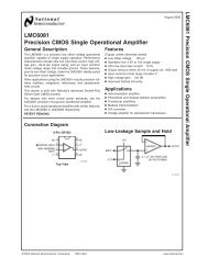
LMC7111 Tiny CMOS Operational Amplifier with Rail-to-Rail Input ...
LMC7111 Tiny CMOS Operational Amplifier with Rail-to-Rail Input ...
LMC7111 Tiny CMOS Operational Amplifier with Rail-to-Rail Input ...

Create successful ePaper yourself
Turn your PDF publications into a flip-book with our unique Google optimized e-Paper software.
<strong>LMC7111</strong><br />
<strong>Tiny</strong> <strong>CMOS</strong> <strong>Operational</strong> <strong>Amplifier</strong> <strong>with</strong> <strong>Rail</strong>-<strong>to</strong>-<strong>Rail</strong> <strong>Input</strong><br />
and Output<br />
General Description<br />
The <strong>LMC7111</strong> is a micropower <strong>CMOS</strong> operational amplifier<br />
available in the space saving SOT 23-5 package. This<br />
makes the <strong>LMC7111</strong> ideal for space and weight critical designs.<br />
The wide common-mode input range makes it easy <strong>to</strong><br />
design battery moni<strong>to</strong>ring circuits which sense signals above<br />
the V + supply. The main benefits of the <strong>Tiny</strong> package are<br />
most apparent in small portable electronic devices, such as<br />
mobile phones, pagers, and portable computers. The tiny<br />
amplifiers can be placed on a board where they are needed,<br />
simplifying board layout.<br />
Features<br />
n <strong>Tiny</strong> 5-Pin SOT23 package saves space<br />
n Very wide common mode input range<br />
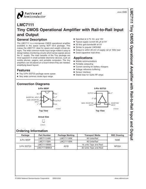
Connection Diagrams<br />
8-Pin MDIP<br />
Top View<br />
Actual Size<br />
01235219<br />
Ordering Information<br />
01235201<br />
n Specified at 2.7V, 5V, and 10V<br />
n Typical supply current 25 µA at 5V<br />
n 50 kHz gain-bandwidth at 5V<br />
n Similar <strong>to</strong> popular LMC6462<br />
n Output <strong>to</strong> <strong>with</strong>in 20 mV of supply rail at 100k load<br />
n Good capacitive load drive<br />
Applications<br />
n Mobile communications<br />
n Portable computing<br />
n Current sensing for battery chargers<br />
n Voltage reference buffering<br />
n Sensor interface<br />
n Stable bias for GaAs RF amps<br />
5-Pin SOT23<br />
Top View<br />
Package Part Number Package Marking Transport Media NSC Drawing<br />
8-Pin MDIP<br />
5-Pin SOT23<br />
<strong>LMC7111</strong>AIN <strong>LMC7111</strong>AIN 40 Units/<strong>Rail</strong><br />
<strong>LMC7111</strong>BIN <strong>LMC7111</strong>BIN 40 Units/<strong>Rail</strong><br />
<strong>LMC7111</strong>BIM5<br />
<strong>LMC7111</strong>BIM5X<br />
A01B<br />
1k units Tape and Reel<br />
3k Units Tape and Reel<br />
01235202<br />
June 2006<br />
N08E<br />
MF05A<br />
<strong>LMC7111</strong> <strong>Tiny</strong> <strong>CMOS</strong> <strong>Operational</strong> <strong>Amplifier</strong> <strong>with</strong> <strong>Rail</strong>-<strong>to</strong>-<strong>Rail</strong> <strong>Input</strong> and Output<br />
© 2006 National Semiconduc<strong>to</strong>r Corporation DS012352 www.national.com
<strong>LMC7111</strong><br />
Absolute Maximum Ratings (Note 1)<br />
If Military/Aerospace specified devices are required,<br />
please contact the National Semiconduc<strong>to</strong>r Sales Office/<br />
Distribu<strong>to</strong>rs for availability and specifications.<br />
Lead Temp. (Soldering, 10 sec.)<br />
S<strong>to</strong>rage Temperature Range<br />
Junction Temperature (Note 4)<br />
260˚C<br />
−65˚C <strong>to</strong> +150˚C<br />
150˚C<br />
ESD Tolerance (Note 2)<br />
SOT23 Package<br />
2000V<br />
MDIP Package<br />
1500V<br />
Differential <strong>Input</strong> Voltage<br />
±Supply Voltage<br />
Voltage at <strong>Input</strong>/Output Pin (V + ) + 0.3V, (V − ) − 0.3V<br />
Supply Voltage (V + −V − )<br />
11V<br />
Current at <strong>Input</strong> Pin<br />
±5 mA<br />
Current at Output Pin (Note 3)<br />
±30 mA<br />
Current at Power Supply Pin<br />
30 mA<br />
Operating Ratings (Note 1)<br />
Supply Voltage<br />
2.5V ≤ V + ≤ 11V<br />
Junction Temperature Range<br />
<strong>LMC7111</strong>AI, <strong>LMC7111</strong>BI<br />
−40˚C ≤ T J ≤ +85˚C<br />
Thermal Resistance (θ JA )<br />
8-Pin MDIP<br />
115˚C/W<br />
5-Pin SOT23<br />
325˚C/W<br />
2.7V DC Electrical Characteristics<br />
Unless otherwise specified, all limits guaranteed for T J = 25˚C, V + = 2.7V, V − = 0V, V CM =V O =V + /2 and R L<br />
> 1MΩ. Boldface<br />
limits apply at the temperature extremes.<br />
Typ <strong>LMC7111</strong>AI <strong>LMC7111</strong>BI<br />
Symbol Parameter Conditions (Note 5) Limit Limit Units<br />
(Note 6) (Note 6)<br />
V OS <strong>Input</strong> Offset Voltage V + = 2.7V 0.9 3 7 mV<br />
5 9 max<br />
TCV OS <strong>Input</strong> Offset Voltage 2.0 µV/˚C<br />
Average Drift<br />
I B <strong>Input</strong> Bias Current (Note 9) 0.1 1 1 pA<br />
20 20 max<br />
I OS <strong>Input</strong> Offset Current (Note 9) 0.01 0.5 0.5 pA<br />
10 10 max<br />
R IN <strong>Input</strong> Resistance >10 Tera Ω<br />
+PSRR Positive Power Supply 2.7V ≤ V + ≤5.0V, 60 55 55 dB<br />
Rejection Ratio V − = 0V, V O = 2.5V 50 50 min<br />
−PSRR Negative Power Supply −2.7V ≤ V − ≤−5.0V, 60 55 55 dB<br />
Rejection Ratio V − = 0V, V O = 2.5V 50 50 min<br />
V CM <strong>Input</strong> Common-Mode V + = 2.7V −0.10 0.0 0.0 V<br />
Voltage Range For CMRR ≥ 50 dB 0.40 0.40 min<br />
2.8 2.7 2.7 V<br />
2.25 2.25 max<br />
C IN Common-Mode <strong>Input</strong> 3 pF<br />
Capacitance<br />
V O Output Swing V + = 2.7V 2.69 2.68 2.68 V<br />
R L = 100 kΩ 2.4 2.4 min<br />
0.01 0.02 0.02 V<br />
0.08 0.08 max<br />
V + = 2.7V 2.65 2.6 2.6 V<br />
R L =10kΩ 2.4 2.4 min<br />
0.03 0.1 0.1 V<br />
0.3 0.3 max<br />
I SC Output Short Circuit Sourcing, V O =0V 7 1 1 mA<br />
Current 0.7 0.7 min<br />
Sinking, V O = 2.7V 7 1 1 mA<br />
0.7 0.7 min<br />
www.national.com 2
2.7V DC Electrical Characteristics (Continued)<br />
Unless otherwise specified, all limits guaranteed for T J = 25˚C, V + = 2.7V, V − = 0V, V CM =V O =V + /2 and R L<br />
> 1MΩ. Boldface<br />
limits apply at the temperature extremes.<br />
Typ <strong>LMC7111</strong>AI <strong>LMC7111</strong>BI<br />
Symbol Parameter Conditions (Note 5) Limit Limit Units<br />
(Note 6) (Note 6)<br />
A VOL Voltage Gain Sourcing 400 V/mv<br />
min<br />
Sinking 150 V/mv<br />
min<br />
I S Supply Current V + = +2.7V, 20 45 50 µA<br />
V O =V + /2 60 65 max<br />
<strong>LMC7111</strong><br />
2.7V AC Electrical Characteristics<br />
Unless otherwise specified, all limits guaranteed for T J = 25˚C, V + = 2.7V, V − = 0V, V CM =V O =V + /2 and R L<br />
> 1MΩ. Boldface<br />
limits apply at the temperature extremes.<br />
Typ <strong>LMC7111</strong>AI <strong>LMC7111</strong>BI<br />
Symbol Parameter Conditions (Note 5) Limit Limit Units<br />
(Note 6) (Note 6)<br />
SR Slew Rate (Note 8) 0.015 V/µs<br />
GBW Gain-Bandwidth Product 40 kHz<br />
Note 1: Absolute Maximum Ratings indicate limits beyond which damage <strong>to</strong> the device may occur. Operating Ratings indicate conditions for which the device is<br />
intended <strong>to</strong> be functional, but specific performance is not guaranteed. For guaranteed specifications and the test conditions, see the Electrical Characteristics.<br />
Note 2: Human Body Model is 1.5 kΩ in series <strong>with</strong> 100 pF.<br />
Note 3: Applies <strong>to</strong> both single-supply and split-supply operation. Continuous short circuit operation at elevated ambient temperature can result in exceeding the<br />
maximum allowed junction temperature at 150˚C.<br />
Note 4: The maximum power dissipation is a function of T J(MAX) , θ JA and T A . The maximum allowable power dissipation at any ambient temperature is P D =<br />
(T J(MAX) −T A )/θ JA . All numbers apply for packages soldered directly in<strong>to</strong> a PC board.<br />
Note 5: Typical Values represent the most likely parametric norm.<br />
Note 6: All limits are guaranteed by testing or statistical analysis.<br />
Note 7: V + = 2.7V, V CM = 1.35V and R L connected <strong>to</strong> 1.35V. For Sourcing tests, 1.35V ≤ V O ≤ 2.7V. For Sinking tests, 0.5V ≤ V O ≤ 1.35V.<br />
Note 8: Connected as Voltage Follower <strong>with</strong> 1.0V step input. Number specified is the slower of the positive and negative slew rates. <strong>Input</strong> referred, V + = 2.7V and<br />
R L = 100 kΩ connected <strong>to</strong> 1.35V. Amp excited <strong>with</strong> 1 kHz <strong>to</strong> produce V O =1V PP .<br />
Note 9: Bias Current guaranteed by design and processing.<br />
3V DC Electrical Characteristics<br />
Unless otherwise specified, all limits guaranteed for T J = 25˚C, V + = 3V, V − = 0V, V CM =V O =V + /2 and R L<br />
> 1MΩ. Boldface<br />
limits apply at the temperature extremes.<br />
Typ <strong>LMC7111</strong>AI <strong>LMC7111</strong>BI<br />
Symbol Parameter Conditions (Note 5) Limit Limit Units<br />
(Note 6) (Note 6)<br />
V CM <strong>Input</strong> Common-Mode V + = 3V −0.25 0.0 0.0 V<br />
Voltage Range For CMRR ≥ 50 dB min<br />
3.2 3.0 3.0 V<br />
2.8 2.8 max<br />
3<br />
www.national.com
<strong>LMC7111</strong><br />
3.3V DC Electrical Characteristics<br />
Unless otherwise specified, all limits guaranteed for T J = 25˚C, V + = 3.3V, V − = 0V, V CM =V O =V + /2 and R L<br />
> 1MΩ. Boldface<br />
limits apply at the temperature extremes.<br />
Typ <strong>LMC7111</strong>AI <strong>LMC7111</strong>BI<br />
Symbol Parameter Conditions (Note 5) Limit Limit Units<br />
(Note 6) (Note 6)<br />
V CM <strong>Input</strong> Common-Mode V + = 3.3V −0.25 −0.1 −0.1 V<br />
Voltage Range For CMRR ≥ 50 dB 0.00 0.00 min<br />
3.5 3.4 3.4 V<br />
3.2 3.2 max<br />
5V DC Electrical Characteristics<br />
Unless otherwise specified, all limits guaranteed for T J = 25˚C, V + = 5V, V − = 0V, V CM =V O =V + /2 and R L<br />
> 1MΩ. Boldface<br />
limits apply at the temperature extremes.<br />
Typ <strong>LMC7111</strong>AI <strong>LMC7111</strong>BI<br />
Symbol Parameter Conditions (Note 5) Limit Limit Units<br />
(Note 6) (Note 6)<br />
V OS <strong>Input</strong> Offset Voltage V + = 5V 0.9 mV<br />
max<br />
TCV OS <strong>Input</strong> Offset Voltage 2.0 µV/˚C<br />
Average Drift<br />
I B <strong>Input</strong> Bias Current (Note 9) 0.1 1 1 pA<br />
20 20 max<br />
I OS <strong>Input</strong> Offset Current (Note 9) 0.01 0.5 0.5 pA<br />
10 10 max<br />
R IN <strong>Input</strong> Resistance >10 Tera Ω<br />
CMRR Common Mode 0V ≤ V CM ≤ 5V 85 70 60 dB<br />
Rejection Ratio<br />
min<br />
+PSRR Positive Power Supply 5V ≤ V + ≤10V, 85 70 60 dB<br />
Rejection Ratio V − = 0V, V O = 2.5V min<br />
−PSRR Negative Power Supply −5V ≤ V − ≤−10V, 85 70 60 dB<br />
Rejection Ratio V − = 0V, V O = −2.5V min<br />
V CM <strong>Input</strong> Common-Mode V + = 5V −0.3 −0.20 −0.20 V<br />
Voltage Range For CMRR ≥ 50 dB 0.00 0.00 min<br />
5.25 5.20 5.20 V<br />
5.00 5.00 max<br />
C IN Common-Mode <strong>Input</strong> 3 pF<br />
Capacitance<br />
V O Output Swing V + = 5V 4.99 4.98 4.98 Vmin<br />
R L = 100 kΩ 0.01 0.02 0.02 Vmax<br />
V + = 5V 4.98 4.9 4.9 Vmin<br />
R L =10kΩ 0.02 0.1 0.1 Vmin<br />
I SC Output Short Circuit Sourcing, V O =0V 7 5 5 mA<br />
Current 3.5 3.5 min<br />
Sinking, V O =3V 7 5 5 mA<br />
3.5 3.5 min<br />
A VOL Voltage Gain Sourcing 500 V/mv<br />
min<br />
Sinking 200 V/mv<br />
min<br />
I S Supply Current V + = +5V, 25 µA<br />
V O =V + /2<br />
max<br />
www.national.com 4
5V AC Electrical Characteristics<br />
Unless otherwise specified, all limits guaranteed for T J = 25˚C, V + = 5V, V − = 0V, V CM =V O =V + /2 and R L<br />
> 1MΩ. Boldface<br />
limits apply at the temperature extremes.<br />
Typ <strong>LMC7111</strong>AI <strong>LMC7111</strong>BI<br />
Symbol Parameter Conditions (Note 5) Limit Limit Units<br />
(Note 6) (Note 6)<br />
SR Slew Rate Positive Going Slew Rate 0.027 0.015 0.010 V/µs<br />
(Note 8)<br />
GBW Gain-Bandwidth Product 50 kHz<br />
<strong>LMC7111</strong><br />
Note 10: Absolute Maximum Ratings indicate limits beyond which damage <strong>to</strong> the device may occur. Operating Ratings indicate conditions for which the device is<br />
intended <strong>to</strong> be functional, but specific performance is not guaranteed. For guaranteed specifications and the test conditions, see the Electrical Characteristics.<br />
Note 11: Human body model, 1.5 kΩ in series <strong>with</strong> 100 pF.<br />
Note 12: Applies <strong>to</strong> both single-supply and split-supply operation. Continuous short circuit operation at elevated ambient temperature can result in exceeding the<br />
maximum allowed junction temperature at 150˚C.<br />
Note 13: The maximum power dissipation is a function of T J(max) , θ JA and T A . The maximum allowable power dissipation at any ambient temperature is P D =<br />
(T J(max) −T A )/θ JA . All numbers apply for packages soldered directly in<strong>to</strong> a PC board.<br />
Note 14: Typical Values represent the most likely parametric norm.<br />
Note 15: All limits are guaranteed by testing or statistical analysis.<br />
Note 16: V + =5V,V CM = 2.5V and R L connected <strong>to</strong> 2.5V. For Sourcing tests, 2.5V ≤ V O ≤ 5.0V. For Sinking tests, 0.5V ≤ V O ≤ 2.5V.<br />
Note 17: Connected as Voltage Follower <strong>with</strong> 1.0V step input. Number specified is the slower of the positive slew rate. The negative slew rate is faster. <strong>Input</strong><br />
referred, V + = 5V and R L = 100 kΩ connected <strong>to</strong> 1.5V. Amp excited <strong>with</strong> 1 kHz <strong>to</strong> produce V O =1V PP .<br />
Note 18: Bias Current guaranteed by design and processing.<br />
10V DC Electrical Characteristics<br />
Unless otherwise specified, all limits guaranteed for T J = 25˚C, V + = 10V, V − = 0V, V CM =V O =V + /2 and R L<br />
> 1MΩ. Boldface<br />
limits apply at the temperature extremes.<br />
Typ <strong>LMC7111</strong>AI <strong>LMC7111</strong>BI<br />
Symbol Parameter Conditions (Note 5) Limit Limit Units<br />
(Note 6) (Note 6)<br />
V OS <strong>Input</strong> Offset Voltage V + = 10V 0.9 3 7 mV<br />
5 9 max<br />
TCV OS <strong>Input</strong> Offset Voltage 2.0 µV/˚C<br />
Average Drift<br />
I B <strong>Input</strong> Bias Current 0.1 1 1 pA<br />
20 20 max<br />
I OS <strong>Input</strong> Offset Current 0.01 0.5 0.5 pA<br />
10 10 max<br />
R IN <strong>Input</strong> Resistance >10 Tera Ω<br />
+PSRR Positive Power Supply 5V ≤ V + ≤10V, 80 dB<br />
Rejection Ratio V − = 0V, V O = 2.5V min<br />
−PSRR Negative Power Supply −5V ≤ V − ≤−10V, 80 dB<br />
Rejection Ratio V − = 0V, V O = 2.5V min<br />
V CM <strong>Input</strong> Common-Mode V + = 10V −0.2 −0.15 −0.15 V<br />
Voltage Range For CMRR ≥ 50 dB 0.00 0.00 min<br />
10.2 10.15 10.15 V<br />
10.00 10.00 max<br />
C IN Common-Mode <strong>Input</strong> 3 pF<br />
Capacitance<br />
I SC Output Short Circuit Sourcing, V O =0V 30 20 20 mA<br />
Current (Note 9) 7 7 min<br />
Sinking, V O = 10V 30 20 20 mA<br />
7 7 min<br />
5<br />
www.national.com
<strong>LMC7111</strong><br />
10V DC Electrical Characteristics (Continued)<br />
Unless otherwise specified, all limits guaranteed for T J = 25˚C, V + = 10V, V − = 0V, V CM =V O =V + /2 and R L<br />
> 1MΩ. Boldface<br />
limits apply at the temperature extremes.<br />
Typ <strong>LMC7111</strong>AI <strong>LMC7111</strong>BI<br />
Symbol Parameter Conditions (Note 5) Limit Limit Units<br />
(Note 6) (Note 6)<br />
A VOL Voltage Gain Sourcing 500 V/mv<br />
100 kΩ Load min<br />
Sinking 200 V/mv<br />
min<br />
I S Supply Current V + = +10V, 25 50 60 µA<br />
V O =V + /2 65 75 max<br />
V O Output Swing V + = 10V 9.99 9.98 9.98 Vmin<br />
R L = 100 kΩ 0.01 0.02 0.02 Vmax<br />
V + = 10V 9.98 9.9 9.9 Vmin<br />
R L =10kΩ 0.02 0.1 0.1 Vmin<br />
10V AC Electrical Characteristics<br />
Unless otherwise specified, all limits guaranteed for T J = 25˚C, V + = 10V, V − = 0V, V CM =V O =V + /2 and R L<br />
> 1MΩ. Boldface<br />
limits apply at the temperature extremes.<br />
Typ <strong>LMC7111</strong>AI <strong>LMC7111</strong>BI<br />
Symbol Parameter Conditions (Note 5) Limit Limit Units<br />
(Note 6) (Note 6)<br />
SR Slew Rate (Note 8) 0.03 V/µs<br />
GBW Gain-Bandwidth Product 50 kHz<br />
φ m Phase Margin 50 deg<br />
G m Gain Margin 15 dB<br />
<strong>Input</strong>-Referred f = 1 kHz 110<br />
Voltage Noise V CM =1V<br />
<strong>Input</strong>-Referred f = 1 kHz 0.03<br />
Current Noise<br />
Note 19: Absolute Maximum Ratings indicate limits beyond which damage <strong>to</strong> the device may occur. Operating Ratings indicate conditions for which the device is<br />
intended <strong>to</strong> be functional, but specific performance is not guaranteed. For guaranteed specifications and the test conditions, see the Electrical Characteristics.<br />
Note 20: Human body model, 1.5 kΩ in series <strong>with</strong> 100 pF.<br />
Note 21: Applies <strong>to</strong> both single-supply and split-supply operation. Continuous short circuit operation at elevated ambient temperature can result in exceeding the<br />
maximum allowed junction temperature at 150˚C.<br />
Note 22: The maximum power dissipation is a function of T J(max) , θ JA and T A . The maximum allowable power dissipation at any ambient temperature is P D =<br />
(T J(max) −T A )/θ JA . All numbers apply for packages soldered directly in<strong>to</strong> a PC board.<br />
Note 23: Typical Values represent the most likely parametric norm.<br />
Note 24: All limits are guaranteed by testing or statistical analysis.<br />
Note 25: V + = 10V, V CM = 5V and R L connected <strong>to</strong> 5V. For Sourcing tests, 5V ≤ V O ≤ 10V. For Sinking tests, 0.5V ≤ V O ≤ 5V.<br />
Note 26: Connected as Voltage Follower <strong>with</strong> 1.0V step input. Number specified is the slower of the positive and negative slew rates. <strong>Input</strong> referred, V + = 10V and<br />
R L = 100 kΩ connected <strong>to</strong> 5V. Amp excited <strong>with</strong> 1 kHz <strong>to</strong> produce V O =2V PP .<br />
Note 27: Operation near absolute maximum limits will adversely affect reliability.<br />
www.national.com 6
Typical Performance Characteristics<br />
T A = 25˚C unless specified, Single Supply<br />
<strong>LMC7111</strong><br />
Supply Current vs. Supply Voltage<br />
Voltage Noise vs. Frequency<br />
01235203<br />
01235204<br />
2.7V Performance<br />
Offset Voltage vs. Common Mode Voltage @ 2.7V<br />
Sinking Output vs. Output Voltage<br />
01235268<br />
01235220<br />
Sourcing Output vs. Output Voltage Gain and Phase vs. Capacitive Load @ 2.7V<br />
01235221 01235222<br />
7<br />
www.national.com
<strong>LMC7111</strong><br />
2.7V Performance (Continued)<br />
Gain and Phase vs. Capacitive Load @ 2.7V Gain and Phase vs. Capacitive Load @ 2.7V<br />
01235223 01235224<br />
3V Performance<br />
Voltage Noise vs. Common Mode Voltage @ 3V<br />
Output Voltage vs. <strong>Input</strong> Voltage @ 3V<br />
01235225 01235226<br />
Offset Voltage vs. Common Mode Voltage @ 3V<br />
Sourcing Output vs. Output Voltage<br />
01235227<br />
01235228<br />
www.national.com 8
3V Performance (Continued)<br />
Sinking Output vs. Output Voltage<br />
Gain and Phase vs. Capacitive Load @ 3V<br />
<strong>LMC7111</strong><br />
01235229 01235230<br />
Gain and Phase vs. Capacitive Load @ 3V<br />
Gain and Phase vs. Capacitive Load @ 3V<br />
01235231 01235232<br />
5V Performance<br />
Voltage Noise vs. Common Mode Voltage @ 5V<br />
Output Voltage vs. <strong>Input</strong> Voltage @ 5V<br />
01235233 01235234<br />
9<br />
www.national.com
<strong>LMC7111</strong><br />
5V Performance (Continued)<br />
Offset Voltage vs. Common Mode Voltage @ 5V<br />
Sourcing Output vs. Output Voltage<br />
01235235<br />
01235236<br />
Sinking Output vs. Output Voltage<br />
Gain and Phase vs. Capacitive Load @ 5V<br />
01235237 01235238<br />
Gain and Phase vs. Capacitive Load @ 5V<br />
Gain and Phase vs. Capacitive Load @ 5V<br />
01235239 01235240<br />
www.national.com 10
5V Performance (Continued)<br />
Non-Inverting Small Signal Pulse Response at 5V<br />
Non-Inverting Small Signal Pulse Response at 5V<br />
<strong>LMC7111</strong><br />
01235241 01235242<br />
Non-Inverting Small Signal Pulse Response at 5V<br />
Non-Inverting Large Signal Pulse Response at 5V<br />
01235243 01235244<br />
Non-Inverting Large Signal Pulse Response at 5V<br />
Non-Inverting Large Signal Pulse Response at 5V<br />
01235245 01235246<br />
11<br />
www.national.com
<strong>LMC7111</strong><br />
5V Performance (Continued)<br />
Inverting Small Signal Pulse Response at 5V<br />
Inverting Small Signal Pulse Response at 5V<br />
01235247 01235248<br />
Inverting Small Signal Pulse Response at 5V<br />
Inverting Large Signal Pulse Response at 5V<br />
01235249 01235250<br />
Inverting Large Signal Pulse Response at 5V<br />
Inverting Large Signal Pulse Response at 5V<br />
01235251 01235252<br />
www.national.com 12
10V Performance<br />
Voltage Noise vs. Common Mode Voltage @ 10V<br />
Output Voltage vs. <strong>Input</strong> Voltage @ 10V<br />
<strong>LMC7111</strong><br />
01235253 01235254<br />
Offset Voltage vs. Common Mode Voltage @ 10V<br />
Sourcing Output vs. Output Voltage<br />
01235255<br />
01235256<br />
Sinking Output vs. Output Voltage<br />
Gain and Phase vs. Capacitive Load @ 10V<br />
01235257 01235258<br />
13<br />
www.national.com
<strong>LMC7111</strong><br />
10V Performance (Continued)<br />
Gain and Phase vs. Capacitive Load @ 10V<br />
Gain and Phase vs. Capacitive Load @ 10V<br />
01235259 01235260<br />
Non-Inverting Small Signal Pulse Response at 10V<br />
Non-Inverting Large Signal Pulse Response at 10V<br />
01235261 01235262<br />
Inverting Small Signal Pulse Response at 10V<br />
Inverting Large Signal Pulse Response at 10V<br />
01235263 01235264<br />
www.national.com 14
Application Information<br />
1.0 BENEFITS OF THE <strong>LMC7111</strong><br />
TINY AMP<br />
<strong>LMC7111</strong><br />
Size<br />
The small footprint of the SOT 23-5 packaged <strong>Tiny</strong> amp,<br />
(0.120 x 0.118 inches, 3.05 x 3.00 mm) saves space on<br />
printed circuit boards, and enable the design of smaller<br />
electronic products. Because they are easier <strong>to</strong> carry, many<br />
cus<strong>to</strong>mers prefer smaller and lighter products.<br />
Height<br />
The height (0.056 inches, 1.43 mm) of the <strong>Tiny</strong> amp makes<br />
it possible <strong>to</strong> use it in PCMCIA type III cards.<br />
Signal Integrity<br />
Signals can pick up noise between the signal source and the<br />
amplifier. By using a physically smaller amplifier package,<br />
the <strong>Tiny</strong> amp can be placed closer <strong>to</strong> the signal source,<br />
reducing noise pickup and increasing signal integrity. The<br />
<strong>Tiny</strong> amp can also be placed next <strong>to</strong> the signal destination,<br />
such as a buffer for the reference of an analog <strong>to</strong> digital<br />
converter.<br />
Simplified Board Layout<br />
The <strong>Tiny</strong> amp can simplify board layout in several ways.<br />
First, by placing an amp where amps are needed, instead of<br />
routing signals <strong>to</strong> a dual or quad device, long pc traces may<br />
be avoided.<br />
By using multiple <strong>Tiny</strong> amps instead of duals or quads,<br />
complex signal routing and possibly crosstalk can be reduced.<br />
DIPs available for pro<strong>to</strong>typing<br />
<strong>LMC7111</strong> amplifiers packaged in conventional 8-pin dip<br />
packages can be used for pro<strong>to</strong>typing and evaluation <strong>with</strong>out<br />
the need <strong>to</strong> use surface mounting in early project stages.<br />
Low Supply Current<br />
The typical 25 µA supply current of the <strong>LMC7111</strong> extends<br />
battery life in portable applications, and may allow the reduction<br />
of the size of batteries in some applications.<br />
Wide Voltage Range<br />
The <strong>LMC7111</strong> is characterized at 2.7V, 3V, 3.3V, 5V and 10V.<br />
Performance data is provided at these popular voltages. This<br />
wide voltage range makes the <strong>LMC7111</strong> a good choice for<br />
devices where the voltage may vary over the life of the<br />
batteries.<br />
2.0 INPUT COMMON MODE<br />
VOLTAGE RANGE<br />
The <strong>LMC7111</strong> does not exhibit phase inversion when an<br />
input voltage exceeds the negative supply voltage.<br />
The absolute maximum input voltage is 300 mV beyond<br />
either rail at room temperature. Voltages greatly exceeding<br />
this maximum rating can cause excessive current <strong>to</strong> flow in<br />
or out of the input pins, adversely affecting reliability.<br />
Applications that exceed this rating must externally limit the<br />
maximum input current <strong>to</strong> ±5 mA <strong>with</strong> an input resis<strong>to</strong>r as<br />
shown in Figure 1.<br />
01235214<br />
FIGURE 1. R I <strong>Input</strong> Current Protection for<br />
Voltages Exceeding the Supply Voltage<br />
3.0 CAPACITIVE LOAD TOLERANCE<br />
The <strong>LMC7111</strong> can typically directly drive a 300 pF load <strong>with</strong><br />
V S = 10V at unity gain <strong>with</strong>out oscillating. The unity gain<br />
follower is the most sensitive configuration. Direct capacitive<br />
loading reduces the phase margin of op-amps. The combination<br />
of the op-amp’s output impedance and the capacitive<br />
load induces phase lag. This results in either an underdamped<br />
pulse response or oscillation.<br />
Capacitive load compensation can be accomplished using<br />
resistive isolation as shown in Figure 2. This simple technique<br />
is useful for isolating the capacitive input of multiplexers<br />
and A/D converters.<br />
01235212<br />
FIGURE 2. Resistive Isolation<br />
of a 330 pF Capacitive Load<br />
4.0 COMPENSATING FOR INPUT CAPACITANCE WHEN<br />
USING LARGE VALUE FEEDBACK RESISTORS<br />
When using very large value feedback resis<strong>to</strong>rs, (usually<br />
> 500 kΩ) the large feed back resistance can react <strong>with</strong> the<br />
input capacitance due <strong>to</strong> transducers, pho<strong>to</strong>diodes, and circuit<br />
board parasitics <strong>to</strong> reduce phase margins.<br />
The effect of input capacitance can be compensated for by<br />
adding a feedback capaci<strong>to</strong>r. The feedback capaci<strong>to</strong>r (as in<br />
Figure 3), C f is first estimated by:<br />
or<br />
R 1 C IN ≤ R 2 C f<br />
which typically provides significant overcompensation.<br />
Printed circuit board stray capacitance may be larger or<br />
smaller than that of a breadboard, so the actual optimum<br />
value for C F may be different. The values of C F should be<br />
checked on the actual circuit. (Refer <strong>to</strong> the LMC660 quad<br />
<strong>CMOS</strong> amplifier data sheet for a more detailed discussion.)<br />
15<br />
www.national.com
<strong>LMC7111</strong><br />
Application Information (Continued)<br />
01235213<br />
FIGURE 3. Cancelling the Effect of <strong>Input</strong> Capacitance<br />
5.0 OUTPUT SWING<br />
The output of the <strong>LMC7111</strong> will go <strong>to</strong> <strong>with</strong>in 100 mV of either<br />
power supply rail for a 10 kΩ load and <strong>to</strong> 20 mV of the rail for<br />
a 100 kΩ load. This makes the <strong>LMC7111</strong> useful for driving<br />
transis<strong>to</strong>rs which are connected <strong>to</strong> the same power supply.<br />
By going very close <strong>to</strong> the supply, the <strong>LMC7111</strong> can turn the<br />
transis<strong>to</strong>rs all the way on or all the way off.<br />
6.0 BIASING GaAs RF AMPLIFIERS<br />
The capacitive load capability, low current draw, and small<br />
size of the SOT23-5 <strong>LMC7111</strong> make it a good choice for<br />
providing a stable negative bias <strong>to</strong> other integrated circuits.<br />
The very small size of the <strong>LMC7111</strong> and the LM4040 reference<br />
take up very little board space.<br />
C F and R isolation prevent oscillations when driving capacitive loads.<br />
01235217<br />
FIGURE 4. Stable Negative Bias<br />
7.0 REFERENCE BUFFER FOR A-TO-D CONVERTERS<br />
The <strong>LMC7111</strong> can be used as a voltage reference buffer for<br />
analog-<strong>to</strong>-digital converters. This works best for A-<strong>to</strong>-D converters<br />
whose reference input is a static load, such as dual<br />
slope integrating A-<strong>to</strong>-Ds. Converters whose reference input<br />
is a dynamic load (the reference current changes <strong>with</strong> time)<br />
may need a faster device, such as the LMC7101 or the<br />
LMC7131.<br />
The small size of the <strong>LMC7111</strong> allows it <strong>to</strong> be placed close <strong>to</strong><br />
the reference input. The low supply current (25 µA typical)<br />
saves power.<br />
For A-<strong>to</strong>-D reference inputs which require higher accuracy<br />
and lower offset voltage, please see the LMC6462<br />
datasheet. The LMC6462 has performance similar <strong>to</strong> the<br />
<strong>LMC7111</strong>. The LMC6462 is available in two grades <strong>with</strong><br />
reduced input voltage offset.<br />
01235218<br />
www.national.com 16
Application Information (Continued)<br />
8.0 DUAL AND QUAD DEVICES WITH SIMILAR<br />
PERFORMANCE<br />
The LMC6462 and LMC6464 are dual and quad devices <strong>with</strong><br />
performance similar <strong>to</strong> the <strong>LMC7111</strong>. They are available in<br />
both conventional through-hole and surface mount packaging.<br />
Please see the LMC6462/4 datasheet for details.<br />
9.0 SPICE MACROMODEL<br />
A SPICE macromodel is available for the <strong>LMC7111</strong>. This<br />
model includes simulation of:<br />
• <strong>Input</strong> common-mode voltage range<br />
• Frequency and transient response<br />
• Quiescent and dynamic supply current<br />
• Output swing dependence on loading conditions and<br />
many more characteristics as listed on the macro model<br />
disk. Contact your local National Semiconduc<strong>to</strong>r sales<br />
office <strong>to</strong> obtain an operational amplifier spice model library<br />
disk.<br />
10.0 ADDITIONAL SOT23-5 TINY<br />
DEVICES<br />
National Semiconduc<strong>to</strong>r has additional parts available in the<br />
space saving SOT23 <strong>Tiny</strong> package, including amplifiers,<br />
voltage references, and voltage regula<strong>to</strong>rs. These devices<br />
include —<br />
LMC7101 1 MHz gain-bandwidth rail-<strong>to</strong>-rail input and output<br />
amplifier — high input impedance and high gain,<br />
700 µA typical current 2.7V, 3V, 5V and 15V<br />
specifications.<br />
LM7131 <strong>Tiny</strong> Video amp <strong>with</strong> 70 MHz gain bandwidth.<br />
Specified at 3V, 5V and ± 5V supplies.<br />
LMC7211 Compara<strong>to</strong>r in a tiny package <strong>with</strong> rail-<strong>to</strong>-rail input<br />
and push-pull output. Typical supply current<br />
of 7 µA. Typical propagation delay of 7 µs. Specified<br />
at 2.7V, 5V and 15V supplies.<br />
LMC7221 Compara<strong>to</strong>r <strong>with</strong> an open drain output for use in<br />
mixed voltage systems. Similar <strong>to</strong> the LMC7211,<br />
except the output can be used <strong>with</strong> a pull-up<br />
resis<strong>to</strong>r <strong>to</strong> a voltage different than the supply<br />
voltage.<br />
LP2980 Micropower SOT 50 mA Ultra Low-Dropout<br />
Regula<strong>to</strong>r.<br />
LM4040<br />
Precision micropower shunt voltage reference.<br />
Fixed voltages of 2.5000V, 4.096V, 5.000V,<br />
8.192V and 10.000V.<br />
LM4041 Precision micropower shunt voltage reference<br />
1.225V and adjustable.<br />
Contact your National Semiconduc<strong>to</strong>r representative for the<br />
latest information.<br />
<strong>LMC7111</strong><br />
17<br />
www.national.com
<strong>LMC7111</strong><br />
SOT-23-5 Tape and Reel<br />
Specification<br />
TAPE FORMAT<br />
Tape Section # Cavities Cavity Status Cover Tape Status<br />
Leader 0 (min) Empty Sealed<br />
(Start End) 75 (min) Empty Sealed<br />
Carrier 3000 Filled Sealed<br />
1000 Filled Sealed<br />
Trailer 125 (min) Empty Sealed<br />
(Hub End) 0 (min) Empty Sealed<br />
TAPE DIMENSIONS<br />
01235215<br />
8 mm 0.130 0.124 0.130 0.126 0.138 ±0.002 0.055 ±0.004 0.157 0.315 ±0.012<br />
(3.3) (3.15) (3.3) (3.2) (3.5 ±0.05) (1.4 ±0.11) (4) (8 ±0.3)<br />
Tape Size DIM A DIM Ao DIM B DIM Bo DIM F DIM Ko DIM P1 DIM W<br />
www.national.com 18
SOT-23-5 Tape and Reel<br />
Specification (Continued)<br />
REEL DIMENSIONS<br />
<strong>LMC7111</strong><br />
01235216<br />
8 mm 7.00 0.059 0.512 0.795 2.165 0.331 + 0.059/−0.000 0.567 W1+ 0.078/−0.039<br />
330.00 1.50 13.00 20.20 55.00 8.40 + 1.50/−0.00 14.40 W1 + 2.00/−1.00<br />
Tape Size A B C D N W1 W2 W3<br />
19<br />
www.national.com
<strong>LMC7111</strong><br />
Physical Dimensions inches (millimeters)<br />
unless otherwise noted<br />
5-Pin SOT23<br />
NS Package Number MF05A<br />
8-Pin Molded DIP<br />
8-Lead (0.300" Wide) Molded Dual-In-Line Package<br />
NS Package Number N08E<br />
www.national.com 20
Notes<br />
National does not assume any responsibility for use of any circuitry described, no circuit patent licenses are implied and National reserves<br />
the right at any time <strong>with</strong>out notice <strong>to</strong> change said circuitry and specifications.<br />
For the most current product information visit us at www.national.com.<br />
LIFE SUPPORT POLICY<br />
NATIONAL’S PRODUCTS ARE NOT AUTHORIZED FOR USE AS CRITICAL COMPONENTS IN LIFE SUPPORT DEVICES OR SYSTEMS<br />
WITHOUT THE EXPRESS WRITTEN APPROVAL OF THE PRESIDENT AND GENERAL COUNSEL OF NATIONAL SEMICONDUCTOR<br />
CORPORATION. As used herein:<br />
1. Life support devices or systems are devices or systems<br />
which, (a) are intended for surgical implant in<strong>to</strong> the body, or<br />
(b) support or sustain life, and whose failure <strong>to</strong> perform when<br />
properly used in accordance <strong>with</strong> instructions for use<br />
provided in the labeling, can be reasonably expected <strong>to</strong> result<br />
in a significant injury <strong>to</strong> the user.<br />
2. A critical component is any component of a life support<br />
device or system whose failure <strong>to</strong> perform can be reasonably<br />
expected <strong>to</strong> cause the failure of the life support device or<br />
system, or <strong>to</strong> affect its safety or effectiveness.<br />
BANNED SUBSTANCE COMPLIANCE<br />
National Semiconduc<strong>to</strong>r follows the provisions of the Product Stewardship Guide for Cus<strong>to</strong>mers (CSP-9-111C2) and Banned Substances<br />
and Materials of Interest Specification (CSP-9-111S2) for regula<strong>to</strong>ry environmental compliance. Details may be found at:<br />
www.national.com/quality/green.<br />
Lead free products are RoHS compliant.<br />
<strong>LMC7111</strong> <strong>Tiny</strong> <strong>CMOS</strong> <strong>Operational</strong> <strong>Amplifier</strong> <strong>with</strong> <strong>Rail</strong>-<strong>to</strong>-<strong>Rail</strong> <strong>Input</strong> and Output<br />
National Semiconduc<strong>to</strong>r<br />
Americas Cus<strong>to</strong>mer<br />
Support Center<br />
Email: new.feedback@nsc.com<br />
Tel: 1-800-272-9959<br />
www.national.com<br />
National Semiconduc<strong>to</strong>r<br />
Europe Cus<strong>to</strong>mer Support Center<br />
Fax: +49 (0) 180-530 85 86<br />
Email: europe.support@nsc.com<br />
Deutsch Tel: +49 (0) 69 9508 6208<br />
English Tel: +44 (0) 870 24 0 2171<br />
Français Tel: +33 (0) 1 41 91 8790<br />
National Semiconduc<strong>to</strong>r<br />
Asia Pacific Cus<strong>to</strong>mer<br />
Support Center<br />
Email: ap.support@nsc.com<br />
National Semiconduc<strong>to</strong>r<br />
Japan Cus<strong>to</strong>mer Support Center<br />
Fax: 81-3-5639-7507<br />
Email: jpn.feedback@nsc.com<br />
Tel: 81-3-5639-7560