74VHC373 - Fairchild Semiconductor
74VHC373 - Fairchild Semiconductor
74VHC373 - Fairchild Semiconductor

You also want an ePaper? Increase the reach of your titles
YUMPU automatically turns print PDFs into web optimized ePapers that Google loves.
<strong>74VHC373</strong><br />
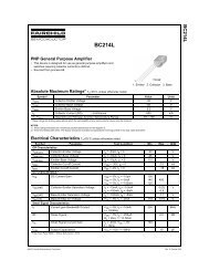
Octal D-Type Latch with 3-STATE Outputs<br />
Features<br />
■ High Speed: t PD = 5.0ns (typ) @ V CC = 5V<br />
■ High Noise Immunity: V NIH = V NIL = 28% V CC (Min.)<br />
■ Power Down Protection is provided on all inputs<br />
■ Low Noise: V OLP = 0.6V (Typ.)<br />
■ Low Power Dissipation: I CC = 4µA (Max) @ T A = 25°C<br />
■ Pin and Function Compatible with 74HC373<br />
General Description<br />
April 2007<br />
The VHC373 is an advanced high speed CMOS octal<br />
D-type latch with 3-STATE output fabricated with silicon<br />
gate CMOS technology. It achieves the high speed operation<br />
similar to equivalent Bipolar Schottky TTL while<br />
maintaining the CMOS low power dissipation. This 8-bit<br />
D-type latch is controlled by a latch enable input (LE)<br />
and an output enable input (OE). The latches appear<br />
transparent to data when latch enable (LE) is HIGH.<br />
When LE is LOW, the data that meets the setup time is<br />
LATCHED. When the OE input is HIGH, the eight<br />
outputs are in a high impedance state.<br />
An input protection circuit ensures that 0V to 7V can be<br />
applied to the input pins without regard to the supply<br />
voltage. This device can be used to interface 5V to 3V<br />
systems and two supply systems such as battery back<br />
up. This circuit prevents device destruction due to mismatched<br />
supply and input voltages.<br />
tm<br />
<strong>74VHC373</strong> Octal D-Type Latch with 3-STATE Outputs<br />
Ordering Information<br />
Order Number<br />
Package<br />
Number<br />
Package Description<br />
<strong>74VHC373</strong>M M20B 20-Lead Small Outline Integrated Circuit (SOIC), JEDEC MS-013, 0.300" Wide<br />
<strong>74VHC373</strong>SJ M20D 20-Lead Small Outline Package (SOP), EIAJ TYPE II, 5.3mm Wide<br />
<strong>74VHC373</strong>MTC MTC20 20-Lead Thin Shrink Small Outline Package (TSSOP), JEDEC MO-153, 4.4mm<br />
Wide<br />
Surface mount packages are also available on Tape and Reel. Specify by appending the suffix letter “X” to the<br />
ordering number. Pb-Free package per JEDEC J-STD-020B.<br />
Connection Diagram<br />
Pin Descriptions<br />
Pin Names<br />
D 0 –D 7<br />
LE<br />
OE<br />
O 0 –O 7<br />
Description<br />
Data Inputs<br />
Latch Enable Input<br />
Output Enable Input<br />
3-STATE Outputs<br />
©1993 <strong>Fairchild</strong> <strong>Semiconductor</strong> Corporation www.fairchildsemi.com<br />
<strong>74VHC373</strong> Rev. 1.3
Logic Symbol<br />
Truth Table<br />
IEEE/IEC<br />
Inputs<br />
Outputs<br />
LE OE D n O n<br />
X H X Z<br />
H L L L<br />
H L H H<br />
Functional Description<br />
The VHC373 contains eight D-type latches with<br />
3-STATE standard outputs. When the Latch Enable (LE)<br />
input is HIGH, data on the D n inputs enters the latches.<br />
In this condition the latches are transparent, i.e., a latch<br />
output will change state each time its D input changes.<br />
When LE is LOW, the latches store the information that<br />
was present on the D inputs a setup time preceding the<br />
HIGH-to-LOW transition of LE. The 3-STATE standard<br />
outputs are controlled by the Output Enable (OE) input.<br />
When OE is LOW, the standard outputs are in the<br />
2-state mode. When OE is HIGH, the standard outputs<br />
are in the high impedance mode but this does not interfere<br />
with entering new data into the latches.<br />
<strong>74VHC373</strong> Octal D-Type Latch with 3-STATE Outputs<br />
L L X O 0<br />
H = HIGH Voltage Level<br />
L = LOW Voltage Level<br />
Z = High Impedance<br />
X = Immaterial<br />
O 0 = Previous O 0 before HIGH-to-LOW transition of<br />
Latch Enable<br />
Logic Diagram<br />
Please note that this diagram is provided only for the understanding of logic operations and should not be used to<br />
estimate propagation delays.<br />
Figure 1.<br />
©1993 <strong>Fairchild</strong> <strong>Semiconductor</strong> Corporation www.fairchildsemi.com<br />
<strong>74VHC373</strong> Rev. 1.3 2
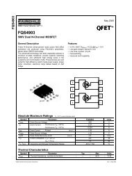
Absolute Maximum Ratings<br />
Stresses exceeding the absolute maximum ratings may damage the device. The device may not function or be<br />
operable above the recommended operating conditions and stressing the parts to these levels is not recommended.<br />
In addition, extended exposure to stresses above the recommended operating conditions may affect device reliability.<br />
The absolute maximum ratings are stress ratings only.<br />
Symbol Parameter Rating<br />
V CC Supply Voltage –0.5V to +7.0V<br />
V IN DC Input Voltage –0.5V to +7.0V<br />
V OUT DC Output Voltage –0.5V to V CC + 0.5V<br />
I IK Input Diode Current –20mA<br />
I OK Output Diode Current ±20mA<br />
I OUT DC Output Current ±25mA<br />
I CC DC V CC /GND Current ±75mA<br />
T STG Storage Temperature –65°C to +150°C<br />
T L Lead Temperature (Soldering, 10 seconds) 260°C<br />
Recommended Operating Conditions (1)<br />
The Recommended Operating Conditions table defines the conditions for actual device operation. Recommended<br />
operating conditions are specified to ensure optimal performance to the datasheet specifications. <strong>Fairchild</strong> does not<br />
recommend exceeding them or designing to absolute maximum ratings.<br />
Symbol Parameter Rating<br />
V CC Supply Voltage 2.0V to +5.5V<br />
V IN Input Voltage 0V to +5.5V<br />
<strong>74VHC373</strong> Octal D-Type Latch with 3-STATE Outputs<br />
V OUT Output Voltage 0V to V CC<br />
T OPR Operating Temperature –40°C to +85°C<br />
t r , t f Input Rise and Fall Time,<br />
V CC = 3.3V ± 0.3V<br />
V CC = 5.0V ± 0.5V<br />
0ns/V ∼ 100ns/V<br />
0ns/V ∼ 20ns/V<br />
Note:<br />
1. Unused inputs must be held HIGH or LOW. They may not float.<br />
©1993 <strong>Fairchild</strong> <strong>Semiconductor</strong> Corporation www.fairchildsemi.com<br />
<strong>74VHC373</strong> Rev. 1.3 3
DC Electrical Characteristics<br />
Symbol Parameter V CC (V) Conditions<br />
V IH<br />
V IL<br />
V OH<br />
V OL<br />
I OZ<br />
I IN<br />
I CC<br />
HIGH Level<br />
Input Voltage<br />
LOW Level Input<br />
Voltage<br />
HIGH Level<br />
Output<br />
Voltage<br />
LOW Level<br />
Output Voltage<br />
3-STATE Output<br />
Off-State<br />
Current<br />
Input Leakage<br />
Current<br />
Quiescent<br />
Supply Current<br />
T A =<br />
25°C –40°C to +85°C<br />
Min. Typ. Max. Min. Max.<br />
2.0 1.50 1.50 V<br />
3.0–5.5 0.7 x V CC 0.7 x V CC<br />
2.0 0.50 0.50 V<br />
3.0–5.5 0.3 x V CC 0.3 x V CC<br />
Units<br />
2.0 V IN = V IH I OH = –50µA 1.9 2.0 1.9 V<br />
3.0 or V IL 2.9 3.0 2.9<br />
4.5 4.4 4.5 4.4<br />
3.0 I OH = –4mA 2.58 2.48<br />
4.5 I OH = –8mA 3.94 3.80<br />
2.0 V IN = V IH I OL = 50µA 0.0 0.1 0.1 V<br />
3.0<br />
or V IL 0.0 0.1 0.1<br />
4.5 0.0 0.1 0.1<br />
3.0 I OL = 4mA 0.36 0.44<br />
4.5 I OL = 8mA 0.36 0.44<br />
5.5 V IN = V IH or V IL ;<br />
V OUT = V CC or GND<br />
±0.25 ±2.5 µA<br />
0–5.5 V IN = 5.5V or GND ±0.1 ±1.0 µA<br />
5.5 V IN = V CC or GND 4.0 40.0 µA<br />
<strong>74VHC373</strong> Octal D-Type Latch with 3-STATE Outputs<br />
Noise Characteristics<br />
Symbol Parameter V CC (V) Conditions<br />
V OLP<br />
(2)<br />
V OLV<br />
(2)<br />
V IHD<br />
(2)<br />
V ILD<br />
(2)<br />
Note:<br />
2. Parameter guaranteed by design.<br />
Typ.<br />
T A = 25°C<br />
Limits<br />
Quiet Output Maximum 5.0 C L = 50pF 0.6 0.9 V<br />
Dynamic V OL<br />
Quiet Output Minimum 5.0 C L = 50pF –0.6 –0.9 V<br />
Dynamic V OL<br />
Minimum HIGH Level<br />
Dynamic Input Voltage<br />
Maximum LOW Level<br />
Dynamic Input Voltage<br />
Units<br />
5.0 C L = 50pF 3.5 V<br />
5.0 C L = 50pF 1.5 V<br />
©1993 <strong>Fairchild</strong> <strong>Semiconductor</strong> Corporation www.fairchildsemi.com<br />
<strong>74VHC373</strong> Rev. 1.3 4
AC Electrical Characteristics<br />
Symbol Parameter V CC (V) Conditions<br />
t PLH , t PHL<br />
t PLH , t PHL<br />
t PZL , t PZH<br />
t PLZ , t PHZ<br />
Propagation Delay<br />
Time (LE to O n )<br />
Propagation Delay<br />
Time (D to O n )<br />
3-STATE Output<br />
Enable Time<br />
3-STATE Output<br />
Disable Time<br />
T A = +25°C<br />
T A = –40°C to<br />
+85°C<br />
Min. Typ. Max. Min. Max.<br />
Notes:<br />
3. Parameter guaranteed by design. t OSLH = |t PLH max – t PLH min |; t OSHL = |t PHL max – t PHL min|<br />
4. C PD is defined as the value of the internal equivalent capacitance which is calculated from the operating<br />
current consumption without load. Average operating current can be obtained by the equation:<br />
I CC (opr.) = C PD • V CC • f IN + I CC /8 (per Latch). The total C PD when n pcs. of the Latch operates can be<br />
calculated by the equation: C PD (total) = 14 + 13n.<br />
Units<br />
3.3 ± 0.3 C L = 15pF 7.0 11.0 1.0 13.0 ns<br />
C L = 50pF 9.5 14.5 1.0 16.5<br />
5.0 ± 0.5 C L = 15pF 4.9 7.2 1.0 8.5 ns<br />
C L = 50pF 6.4 9.2 1.0 10.5<br />
3.3 ± 0.3 C L = 15pF 7.3 11.4 1.0 13.5 ns<br />
C L = 50pF 9.8 14.9 1.0 17.0<br />
5.0 ± 0.5 C L = 15pF 5.0 7.2 1.0 8.5<br />
C L = 50pF 6.5 9.2 1.0 10.5<br />
3.3 ± 0.3 R L = 1kΩ C L = 15pF 7.3 11.4 1.0 13.5 ns<br />
C L = 50pF 9.8 14.9 1.0 17.0<br />
5.0 ± 0.5 C L = 15pF 5.5 8.1 1.0 9.5 ns<br />
C L = 50pF 7.0 10.1 1.0 11.5<br />
3.3 ± 0.3 R L = 1kΩ C L = 50pF 9.5 13.2 1.0 15.0 ns<br />
5.0 ± 0.5 C L = 50pF 6.5 9.2 1.0 10.5<br />
t OSLH , Output to Output 3.3 ± 0.3<br />
(3)<br />
C L = 50pF 1.5 1.5 ns<br />
t OSHL Skew<br />
5.0 ± 0.5 C L = 50pF 1.0 1.0<br />
C IN Input Capacitance V CC = Open 4 10 10 pF<br />
C OUT Output Capacitance V CC = 5.0V 6 pF<br />
C PD Power Dissipation<br />
Capacitance<br />
(4)<br />
27 pF<br />
<strong>74VHC373</strong> Octal D-Type Latch with 3-STATE Outputs<br />
AC Operating Requirements<br />
Symbol Parameter V CC (V)<br />
T A = +25°C<br />
T A = –40°C to +85°C<br />
Min. Typ. Max. Min. Max.<br />
t W (H) Minimum Pulse Width 3.3 ± 0.3 5.0 5.0 ns<br />
(LE)<br />
5.0 ± 0.5 5.0 5.0<br />
t S Minimum Set-Up Time 3.3 ± 0.3 4.0 4.0 ns<br />
5.0 ± 0.5 4.0 4.0<br />
t H Minimum Hold Time 3.3 ± 0.3 1.0 1.0 ns<br />
5.0 ± 0.5 1.0 1.0<br />
Units<br />
©1993 <strong>Fairchild</strong> <strong>Semiconductor</strong> Corporation www.fairchildsemi.com<br />
<strong>74VHC373</strong> Rev. 1.3 5
Physical Dimensions<br />
Dimensions are in inches (millimeters) unless otherwise noted.<br />
<strong>74VHC373</strong> Octal D-Type Latch with 3-STATE Outputs<br />
Figure 2. 20-Lead Small Outline Integrated Circuit (SOIC), JEDEC MS-013, 0.300" Wide<br />
Package Number M20B<br />
©1993 <strong>Fairchild</strong> <strong>Semiconductor</strong> Corporation www.fairchildsemi.com<br />
<strong>74VHC373</strong> Rev. 1.3 6
Physical Dimensions (Continued)<br />
Dimensions are in millimeters unless otherwise noted.<br />
<strong>74VHC373</strong> Octal D-Type Latch with 3-STATE Outputs<br />
Figure 3. 20-Lead Small Outline Package (SOP), EIAJ TYPE II, 5.3mm Wide<br />
Package Number M20D<br />
©1993 <strong>Fairchild</strong> <strong>Semiconductor</strong> Corporation www.fairchildsemi.com<br />
<strong>74VHC373</strong> Rev. 1.3 7
Physical Dimensions (Continued)<br />
Dimensions are in millimeters unless otherwise noted.<br />
<strong>74VHC373</strong> Octal D-Type Latch with 3-STATE Outputs<br />
Figure 4. 20-Lead Thin Shrink Small Outline Package (TSSOP), JEDEC MO-153, 4.4mm Wide<br />
Package Number MTC20<br />
©1993 <strong>Fairchild</strong> <strong>Semiconductor</strong> Corporation www.fairchildsemi.com<br />
<strong>74VHC373</strong> Rev. 1.3 8
TRADEMARKS<br />
The following are registered and unregistered trademarks <strong>Fairchild</strong> <strong>Semiconductor</strong> owns or is authorized to use and is not intended to be an<br />
exhaustive list of all such trademarks.<br />
ACEx ®<br />
Across the board. Around the world.<br />
ActiveArray<br />
Bottomless<br />
Build it Now<br />
CoolFET<br />
CROSSVOLT<br />
CTL<br />
Current Transfer Logic<br />
DOME<br />
E 2 CMOS<br />
EcoSPARK ®<br />
EnSigna<br />
FACT Quiet Series<br />
FACT ®<br />
FAST ®<br />
FASTr<br />
FPS<br />
FRFET ®<br />
GlobalOptoisolator<br />
GTO<br />
HiSeC<br />
i-Lo<br />
ImpliedDisconnect<br />
IntelliMAX<br />
ISOPLANAR<br />
MICROCOUPLER<br />
MicroPak<br />
MICROWIRE<br />
MSX<br />
MSXPro<br />
OCX<br />
OCXPro<br />
OPTOLOGIC ®<br />
OPTOPLANAR ®<br />
PACMAN<br />
POP<br />
Power220 ®<br />
Power247 ®<br />
PowerEdge<br />
PowerSaver<br />
PowerTrench ®<br />
Programmable Active Droop<br />
QFET ®<br />
QS<br />
QT Optoelectronics<br />
Quiet Series<br />
RapidConfigure<br />
RapidConnect<br />
ScalarPump<br />
SMART START<br />
SPM ®<br />
STEALTH<br />
SuperFET<br />
SuperSOT-3<br />
SuperSOT-6<br />
SuperSOT-8<br />
SyncFET<br />
TCM<br />
The Power Franchise ®<br />
<br />
TinyBoost<br />
TinyBuck<br />
TinyLogic ®<br />
TINYOPTO<br />
TinyPower<br />
TinyWire<br />
TruTranslation<br />
SerDes<br />
UHC ®<br />
UniFET<br />
VCX<br />
Wire<br />
<strong>74VHC373</strong> Octal D-Type Latch with 3-STATE Outputs<br />
DISCLAIMER<br />
FAIRCHILD SEMICONDUCTOR RESERVES THE RIGHT TO MAKE CHANGES WITHOUT FURTHER NOTICE TO ANY PRODUCTS<br />
HEREIN TO IMPROVE RELIABILITY, FUNCTION OR DESIGN. FAIRCHILD DOES NOT ASSUME ANY LIABILITY ARISING OUT OF THE<br />
APPLICATION OR USE OF ANY PRODUCT OR CIRCUIT DESCRIBED HEREIN; NEITHER DOES IT CONVEY ANY LICENSE UNDER<br />
ITS PATENT RIGHTS, NOR THE RIGHTS OF OTHERS. THESE SPECIFICATIONS DO NOT EXPAND THE TERMS OF FAIRCHILD’S<br />
WORLDWIDE TERMS AND CONDITIONS, SPECIFICALLY THE WARRANTY THEREIN, WHICH COVERS THESE PRODUCTS.<br />
LIFE SUPPORT POLICY<br />
FAIRCHILD’S PRODUCTS ARE NOT AUTHORIZED FOR USE AS CRITICAL COMPONENTS IN LIFE SUPPORT DEVICES OR<br />
SYSTEMS WITHOUT THE EXPRESS WRITTEN APPROVAL OF FAIRCHILD SEMICONDUCTOR CORPORATION.<br />
As used herein:<br />
1. Life support devices or systems are devices or systems<br />
which, (a) are intended for surgical implant into the body or<br />
(b) support or sustain life, and (c) whose failure to perform<br />
when properly used in accordance with instructions for use<br />
provided in the labeling, can be reasonably expected to<br />
result in a significant injury of the user.<br />
2. A critical component in any component of a life support,<br />
device, or system whose failure to perform can be<br />
reasonably expected to cause the failure of the life support<br />
device or system, or to affect its safety or effectiveness.<br />
PRODUCT STATUS DEFINITIONS<br />
Definition of Terms<br />
Datasheet Identification Product Status Definition<br />
Advance Information Formative or In Design This datasheet contains the design specifications for product<br />
development. Specifications may change in any manner without notice.<br />
Preliminary First Production This datasheet contains preliminary data; supplementary data will be<br />
published at a later date. <strong>Fairchild</strong> <strong>Semiconductor</strong> reserves the right to<br />
make changes at any time without notice to improve design.<br />
No Identification Needed Full Production This datasheet contains final specifications. <strong>Fairchild</strong> <strong>Semiconductor</strong><br />
reserves the right to make changes at any time without notice to improve<br />
design.<br />
Obsolete Not In Production This datasheet contains specifications on a product that has been<br />
discontinued by <strong>Fairchild</strong> <strong>Semiconductor</strong>. The datasheet is printed for<br />
reference information only.<br />
Rev. I24<br />
©1993 <strong>Fairchild</strong> <strong>Semiconductor</strong> Corporation www.fairchildsemi.com<br />
<strong>74VHC373</strong> Rev. 1.3 9