EEN1016 Electronics I - Faculty of Engineering - Multimedia University
EEN1016 Electronics I - Faculty of Engineering - Multimedia University
EEN1016 Electronics I - Faculty of Engineering - Multimedia University

You also want an ePaper? Increase the reach of your titles
YUMPU automatically turns print PDFs into web optimized ePapers that Google loves.
<strong>EEN1016</strong> <strong>Electronics</strong> I: Appendices<br />
<strong>EEN1016</strong> <strong>Electronics</strong> I<br />
Experiment BE1: Diode Circuits<br />
1.0 Objectives<br />
• To observe the operations <strong>of</strong> a half-wave rectifier and a full-wave bridge rectifier<br />
• To observe the effects <strong>of</strong> shunt capacitance and load resistance on the outputs <strong>of</strong><br />
various rectifier circuits<br />
• To observe the operations <strong>of</strong> several diode clipping circuits<br />
• To observe the operation <strong>of</strong> a diode clamping circuit<br />
2.0 Apparatus<br />
“Diode and Transistor Circuits” experiment board<br />
DC Power Supply<br />
Dual-trace Oscilloscope<br />
Function Generator<br />
Digital Multimeter<br />
Connecting wires<br />
3.0 Introduction<br />
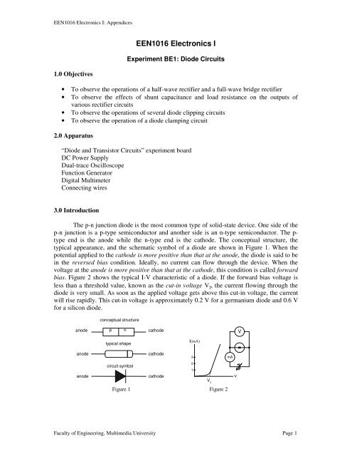
The p-n junction diode is the most common type <strong>of</strong> solid-state device. One side <strong>of</strong> the<br />
p-n junction is a p-type semiconductor and another side is an n-type semiconductor. The p-<br />
type end is the anode while the n-type end is the cathode. The conceptual structure, the<br />
typical appearance, and the schematic symbol <strong>of</strong> a diode are shown in Figure 1. When the<br />
potential applied to the cathode is more positive than that at the anode, the diode is said to be<br />
in the reversed bias condition. Ideally, no current can flow through the device. When the<br />
voltage at the anode is more positive than that at the cathode, this condition is called forward<br />
bias. Figure 2 shows the typical I-V characteristic <strong>of</strong> a diode. If the forward bias voltage is<br />
less than a threshold value, known as the cut-in voltage V γ , the current flowing through the<br />
diode is very small. As soon as the applied voltage gets above this cut-in voltage, the current<br />
will rise rapidly. This cut-in voltage is approximately 0.2 V for a germanium diode and 0.6 V<br />
for a silicon diode.<br />
conceptual structure<br />
anode<br />
p<br />
n<br />
cathode<br />
V<br />
typical shape<br />
I(mA)<br />
anode<br />
anode<br />
cathode<br />
circuit symbol<br />
cathode<br />
3<br />
2<br />
1<br />
V γ<br />
Figure 1 Figure 2<br />
mA<br />
V<br />
<strong>Faculty</strong> <strong>of</strong> <strong>Engineering</strong>, <strong>Multimedia</strong> <strong>University</strong> Page 1
<strong>EEN1016</strong> <strong>Electronics</strong> I: Appendices<br />
Consider a silicon diode that is connected in series with a 1 kΩ resistor, as shown in<br />
Figure 3. When a battery voltage <strong>of</strong> 3 V is applied, the diode is forward-biased and an electric<br />
current will start to flow in both the diode and the resistor. The voltage across the resistor will<br />
rise to a value V R = I×R which is slightly lower than 2.4 V. The current is limited to 2.4 mA<br />
(= 2.4 V/1 kΩ). This voltage will not rise above 2.4 V because otherwise the voltage across<br />
the diode will become lower than 0.6 V, which will then put the diode into a “high<br />
resistance” state that will allow only a very small current to flow in the circuit. Therefore, in<br />
the analysis <strong>of</strong> a diode circuit, we can usually assume the voltage across a silicon diode to be<br />
0.6 V, provided that the voltage source in the circuit is higher than 0.6 V and the polarity is to<br />
bias the diode in the forward direction (forward biased). The diode acts like a switch that is<br />
turned on. If the polarity is reversed, the diode will be reverse-biased and no current can flow<br />
in the circuit. In this condition, the diode acts like a switch that is turned <strong>of</strong>f. As a result, the<br />
voltage across the resistor will become zero (since I = 0).<br />
3V<br />
0.6V<br />
+ -<br />
I<br />
Figure 3<br />
1 kΩ<br />
+<br />
-<br />
V R<br />
Due to the unidirection characteristic <strong>of</strong> the device, a diode can be configured as a<br />
rectifier that allows current flow for only half a cycle <strong>of</strong> an AC waveform. A half-wave<br />
rectifier circuit is shown in Figure 4. When the potential at point A is more positive than that<br />
at point B, i.e. the supply voltage V S is positive, the diode is forward-biased. The voltage<br />
across the resistor will have the same waveform as the supply voltage V S (minus away 0.6V,<br />
to be exact). In the second half cycle, the voltage at A becomes negative, so the diode is<br />
reverse-biased. The voltage across the resistor will be zero throughout this half cycle. As a<br />
result, a half-wave waveform is obtained at the resistor. As the current flows only in the X-to-<br />
Y direction, therefore a direct current is obtained from the AC source.<br />
AC voltage<br />
A<br />
B<br />
+<br />
V S<br />
-<br />
v<br />
X<br />
+ V m<br />
R V o<br />
-<br />
Y φ<br />
Figure 4<br />
π<br />
V S<br />
V o<br />
2 π<br />
ω t<br />
Since the above diode circuit operates only for half a cycle, the efficiency is low. A<br />
bridge-rectifier circuit constructed using 4 diodes, as shown in Figure 5, can be used to<br />
double the efficiency. In the first half cycle <strong>of</strong> an AC waveform, diodes D1 and D2 are turned<br />
on while D3 and D4 are <strong>of</strong>f. Current flows from X to Y. In the second half cycle, when the<br />
potential at point B is more positive than point A, diode D3 and D4 are on while D1 and D3<br />
are turned <strong>of</strong>f. Current flows from X to Y again. Since there is always a current flow during<br />
both the positive cycle and the negative cycle, a rectified full-wave waveform is obtained, as<br />
<strong>Faculty</strong> <strong>of</strong> <strong>Engineering</strong>, <strong>Multimedia</strong> <strong>University</strong> Page 2
<strong>EEN1016</strong> <strong>Electronics</strong> I: Appendices<br />
shown in Figure 5. Note that there is 1.2 V (=2×0.6 V) lost in V o because 2 diodes conduct in<br />
series.<br />
v o<br />
V<br />
m<br />
D 1<br />
& D 2<br />
on<br />
D 3<br />
& D 4<br />
on<br />
D 1<br />
& D 2<br />
on<br />
Figure 5<br />
ω t<br />
A rectifier circuit is usually used to convert an AC voltage into a DC voltage. A<br />
transformer can be connected to the 240 V AC mains supply at the wall outlet to step down<br />
the voltage to a desired level. The large ripples in the half-wave and full-wave rectified<br />
waveforms can be suppressed using a capacitor filter connected in parallel with the load<br />
resistor (see Figure 6). This provides a more stable DC voltage, comparable to a battery, for<br />
operating an electronic system. However, the ripple cannot be totally eliminated. The<br />
amplitude <strong>of</strong> the residual ripple depends on the size <strong>of</strong> the capacitor and the load resistance.<br />
If the load resistance is small, a large capacitance is required to obtain a DC source with<br />
acceptably small ripples.<br />
V m<br />
V 1<br />
Figure 6<br />
Diodes can also be used to change the shape <strong>of</strong> an AC waveform. The circuits in<br />
Figure 7 are known as the clipping circuits. The diodes are turned on for only the period <strong>of</strong><br />
time when the AC voltage is at least 0.6 V higher than the reference voltage, V ref . During this<br />
period, a current flow through the diode and the voltage across the diode is about 0.6 V. As a<br />
result, part <strong>of</strong> the output AC waveform, V o , is clipped <strong>of</strong>f.<br />
+<br />
R<br />
+<br />
-<br />
V S<br />
+<br />
V ref<br />
+<br />
-<br />
V o<br />
V ref - V γ<br />
V ref<br />
+V γ<br />
-<br />
Figure 7(a)<br />
V S<br />
V o<br />
π<br />
2π<br />
ωt<br />
+<br />
R<br />
+<br />
V m - V γ<br />
V m -V γ<br />
V SVo<br />
V S<br />
-<br />
V ref<br />
-<br />
-<br />
V o<br />
V ref<br />
Figure 7(b)<br />
Vref<br />
π<br />
2π<br />
ωt<br />
<strong>Faculty</strong> <strong>of</strong> <strong>Engineering</strong>, <strong>Multimedia</strong> <strong>University</strong> Page 3
<strong>EEN1016</strong> <strong>Electronics</strong> I: Appendices<br />
Another wave shaping circuit, as shown in Figure 8, is the clamping circuit. The<br />
capacitor is fully charged to the peak voltage <strong>of</strong> the AC source when the diode is forwardbiased.<br />
(For simplicity, we have assumed the forward voltage drop <strong>of</strong> the diode is negligible.)<br />
As the diode acts like a switch that is turned on, the output voltage taken across the diode is<br />
zero when the AC waveform is at its peak. As soon as the AC voltage falls below the peak<br />
value, the diode becomes reverse-biased by the voltage sum <strong>of</strong> the transformer and the<br />
capacitor which is a negative value. The resulting waveform is an AC waveform that is<br />
“clamped” down below zero volt. If the 0.6 V forward voltage drop <strong>of</strong> the diode is<br />
considered, the capacitor is charge to (V m – 0.6) V and the average value <strong>of</strong> V o is – (V m – 0.6<br />
) V. The V o peak voltage is 0.6 V above zero volt.<br />
C<br />
+<br />
V m<br />
V S<br />
V S<br />
~<br />
V o<br />
-Vm + 0.6<br />
ωt<br />
-<br />
V o<br />
Instructions<br />
Figure 8<br />
The lab is divided into two parts: Part A Theoretical Prediction and Part B Experiment.<br />
Read through both parts carefully, attempt and prepared for all the questions in both parts.<br />
Students must complete the theoretical predictions before attending the corresponding lab<br />
session. During the processes <strong>of</strong> theoretical predictions, students should attempt to<br />
understand the purposes <strong>of</strong> the experiments. The Short Report Form for Part A has to be<br />
submitted to the Lab’s technician at least two days before the scheduled lab session. The<br />
instructor will check your predictions and then return it back to you during your lab session.<br />
Use the predicted results to verify your measured data. Students are required to submit the<br />
Short Report Form for Part B, attached with Short Report Form for Part A<br />
immediately after the lab session.<br />
Cautions<br />
Oscilloscope: Make sure the INTENSITY <strong>of</strong> the displayed waveforms is not too high,<br />
which can burn the screen material <strong>of</strong> the oscilloscope.<br />
Function generator: Never short-circuit the output (the clip with red sleeve), which may<br />
burn the output stage <strong>of</strong> the function generator.<br />
Sketching oscilloscope waveforms on graph papers<br />
Refer to Appendix D for efficient waveform sketching.<br />
Factors affecting your experiment progress<br />
Your preparation before coming to the lab (your understanding on the theories, the<br />
procedures and the information in the appendices; your planning to carry out the<br />
experiments and to take data), attempt all questions before the lab.<br />
Your understanding on the functions and the operations <strong>of</strong> the equipment (Your learning<br />
on using the equipment during the Induction Program Lab Session; your understanding on<br />
checking and presetting the equipment)<br />
The technique you use to sketch waveforms on graph papers<br />
<strong>Faculty</strong> <strong>of</strong> <strong>Engineering</strong>, <strong>Multimedia</strong> <strong>University</strong> Page 4
<strong>EEN1016</strong> <strong>Electronics</strong> I: Appendices<br />
Part A: Theoretical Predictions<br />
For the cases where V S is a sinusoidal voltage source, apply V S = 10 sin (2π×10000t) V.<br />
4.1 Half-wave Rectifier<br />
1. Use diode forward voltage drop <strong>of</strong> 0.6 V, predict the maximum currents flow through the<br />
diode D1 (I D, max ) in the circuit <strong>of</strong> Experiment 4.1, if R3 = 18 kΩ and 10 kΩ. Record the<br />
values in Table T4.1 <strong>of</strong> the Short Report Form provided.<br />
2. From Appendix E, find the more exact values <strong>of</strong> the diode forward voltage drops (V F ) at<br />
the corresponding maximum currents.<br />
3. Predict the maximum V o voltages (V o, max ) for both cases.<br />
4. Predict the minimum V o voltage (V o,min ).<br />
4.2 Full-wave Rectifier<br />
1. Use diode forward voltage drop <strong>of</strong> 0.6 V, predict the maximum currents flow through the<br />
diodes (I D, max ) in the circuit <strong>of</strong> Experiment 4.2, if R3 = 18 kΩ and 10 kΩ. Note that two<br />
diodes conduct at a time. Record the values in Table T4.2.<br />
2. From Appendix E, find the more exact values <strong>of</strong> the diode forward voltage drops (V F ) at<br />
the corresponding maximum currents.<br />
3. Predict the maximum V o voltages (V o, max ) for both cases.<br />
4. Predict the minimum V o voltage (V o, min ).<br />
4.3 Clipping Circuits<br />
1. Use diode forward voltage drop <strong>of</strong> 0.7 V when V S = 5 to 10 V, 0.65 V when V S = 2 to 4<br />
V and 0.6 V when V S = 1 V, predict the currents flow through the diode (I D ) in Procedure<br />
1 <strong>of</strong> Experiment 4.3 when V S = 1, 2, 3, 5, 10 V. Record the values in Table T4.3 (a).<br />
2. From Appendix E, find the more exact values <strong>of</strong> the diode forward voltage drops (V F ) at<br />
the corresponding diode currents. (Note for more precise results, iteration is required.<br />
Iteration: start with a V F to calculate I D and then find new V F . Use this new V F value to<br />
calculate I D and find another new V F . The process is repeated until subsequent V F values<br />
are about the same.)<br />
3. The set <strong>of</strong> values predicted in the above steps 1 and step 2 can be used to compare with<br />
the sketched waveform in the experimental Procedure 2 <strong>of</strong> Experiment 4.3. Note in this<br />
case V F = V o .<br />
4. Predict the minimum V o voltage (V o,min ).<br />
5. Hence, you have known that the dependence <strong>of</strong> V F on I D . For simplicity, use fixed V F =<br />
0.7 V to predict V o, max and V o¸ min for Procedure 4, Procedure 6 and Procedure 8 <strong>of</strong><br />
Experiment 4.3 for V DC = 0, 2, 4, 6 V. Note that the largest I D in Procedure 8 is (16 –<br />
0.7)/1k = 15.3 mA. Record the values in Table T4.3 (b), Table T4.3 (c) and Table T4.3<br />
(d), respectively.<br />
4.4 Clamping Circuit<br />
1. With fixed V F = 0.7 V, predict V o, max and V o¸ min for Procedure 1 <strong>of</strong> Experiment 4.4 for<br />
V DC = 0, 2, 4, 6 V. Record the values in Table T4.4.<br />
<strong>Faculty</strong> <strong>of</strong> <strong>Engineering</strong>, <strong>Multimedia</strong> <strong>University</strong> Page 5
<strong>EEN1016</strong> <strong>Electronics</strong> I: Appendices<br />
Part B: Experiments<br />
4.0 Diode test<br />
Procedures<br />
Referring to the circuit board layout in Appendix A, without any connections, test all the<br />
diodes on the board by using the go/no-go testing method.<br />
1. Set a multimeter in “diode test” mode (note that some multimeters need to push in two<br />
buttons together to set “diode test” mode as indicated on the control panel). The “COM”<br />
terminal is negative “–“ and the “V, Ω, mA” terminal is positive “+”.<br />
2. Test the diode D1 on the board in forward-biased condition, i.e. connect “+” terminal to<br />
anode the and “–“ to the cathode. A good diode will give forward voltage drop <strong>of</strong> about<br />
0.7 V or 700 mV. Record the reading in Table E4.0.<br />
3. Repeat Procedure 2 for other diodes.<br />
Equipment Setups for Experiments 4.1 to 4.4 (Refer to Appendix C for brief information<br />
or the Induction Program Lab Sheets for more information)<br />
1. Before starting the experiment, check and verify that the equipment (oscilloscope and<br />
function generator) to be used is functioning properly, including voltage probes [see<br />
Appendix B].<br />
2. Set the vertical sensitivities <strong>of</strong> CH1 and CH2 <strong>of</strong> the oscilloscope to 5 V/div. Set the<br />
horizontal (time base) sensitivity to 20 µs/div. Make sure the variable knobs <strong>of</strong> Volt/div<br />
and Time/div at the calibrated (CAL’D) positions. Set the input couplings (AC/GND/DC<br />
switches) <strong>of</strong> CH1 and CH2 to DC. Set the vertical mode to dual waveform display. Set<br />
the trigger source to CH1 and the triggering mode/coupling to AUTO. [For other<br />
presetting, refer to Appendix C]<br />
3. Set the function generator for a 10 kHz sine wave with 10 V amplitude. Check the<br />
waveform using the oscilloscope.<br />
4. Connect the sine wave signal to terminals P1 - P2 (grounded at P2). See the circuit board<br />
layout in Appendix A.<br />
5. Connect a probe from CH1 <strong>of</strong> the oscilloscope to P1 – P2 (grounded at P2).<br />
6. Connect the second probe from CH2 to T9 - P5 (grounded at P5).<br />
7. Carry out the following experiments with these setups.<br />
4.1 Half-wave Rectifier<br />
Procedures<br />
1. Using the circuit board provided, construct the circuit as shown below by connecting T1<br />
to TA5, T2 to TA6, T7 to TA17, T8 to TA18, and T3 to T4.<br />
signal<br />
in<br />
signal<br />
ground<br />
+<br />
–<br />
V I<br />
1 : 1<br />
+<br />
–<br />
V S<br />
D1<br />
R3<br />
+<br />
–<br />
V O<br />
oscilloscope<br />
ground<br />
2. Align the ground levels <strong>of</strong> CH1 and CH2 as indicated in Graph E4.1 (a). Finely adjust the<br />
function generator frequency so that CH1 waveform (V I ) has period <strong>of</strong> 5 divisions (5 div<br />
x 20 µs/div = 100 µs which is approximately equal to 1/f gen , where f gen is the frequency<br />
<strong>Faculty</strong> <strong>of</strong> <strong>Engineering</strong>, <strong>Multimedia</strong> <strong>University</strong> Page 6
<strong>EEN1016</strong> <strong>Electronics</strong> I: Appendices<br />
reading displayed on the function generator). Adjust the oscilloscope trigger level and the<br />
CH1 horizontal position so that CH1 waveform has peaks at the positions as shown in<br />
Graph E4.1 (a). This step is important for V o waveform to be drawn with respect to V I<br />
waveform. Keep the oscilloscope ON all the time because it needs to be warmed up.<br />
3. Sketch the CH2 waveform (V o ) displayed on the oscilloscope on Graph E4.1 (a). Do not<br />
move the waveform positions during the sketching. Measure the maximum and the<br />
minimum voltages <strong>of</strong> CH2 waveform (V o, max and V o, min ) and record them in Table E4.1<br />
(under column header: Procedure 3). Calculate the ripple voltage, V o,r = V o, max – V o,min .<br />
4. Repeat Procedure 3 for the following conditions at the rectifier output. Sketch the<br />
required V o waveforms on their corresponding graphs and record all the respective V o, max<br />
and V o, min in their corresponding columns in Table E4.1.<br />
(i) C3 (10 nF) and R3 (18 kΩ) in parallel (sketch V o waveform)<br />
(ii) C3 and R2 (10 kΩ) in parallel<br />
(iii) C2 (470 pF) and R3 in parallel (sketch V o waveform)<br />
(iv) C3 alone<br />
(v) C2 alone (sketch V o waveform)<br />
Ask the instructor to check your results. Show all the sketched waveforms, Table E4.1<br />
readings and the waveforms <strong>of</strong> Procedure 4 (v) displayed on the oscilloscope.<br />
4.2 Full-wave Rectifier<br />
Procedures<br />
1. Construct the circuit as shown below.<br />
signal<br />
in<br />
+<br />
–<br />
signal<br />
ground<br />
V I<br />
1 : 1<br />
+<br />
–<br />
V S<br />
D3<br />
D5<br />
D6<br />
D4<br />
R3<br />
+<br />
–<br />
V O<br />
oscilloscope oscillascope<br />
ground<br />
2. Align the channel ground levels. Adjust and align the CH1 waveform as mentioned in<br />
Procedure 2 <strong>of</strong> Experiment 4.1.<br />
3. Sketch V o waveform displayed on the oscilloscope on Graph E4.2 (a). Measure V o, max<br />
and V o, min and record them in Table E4.2. Calculate V o,r = V o, max – V o,min .<br />
4. Repeat Procedure 3 for the following conditions at the rectifier output. Sketch the<br />
required V o waveforms on their corresponding graphs and record all the respective V o, max<br />
and V o, min in their corresponding columns in Table E4.2.<br />
(i) C3 (10 nF) and R3 (18 kΩ) in parallel (sketch V o waveform)<br />
(ii) C3 and R2 (10 kΩ) in parallel<br />
(iii) C2 (470 pF) and R3 in parallel (sketch V o waveform)<br />
(iv) C3 alone<br />
(v) C2 alone (sketch V o waveform)<br />
Ask the instructor to check your results. Show all the sketched waveforms, Table E4.2<br />
readings and the waveforms <strong>of</strong> Procedure 4 (v) displayed on the oscilloscope.<br />
<strong>Faculty</strong> <strong>of</strong> <strong>Engineering</strong>, <strong>Multimedia</strong> <strong>University</strong> Page 7
<strong>EEN1016</strong> <strong>Electronics</strong> I: Appendices<br />
4.3 Clipping Circuits<br />
Procedures<br />
1. Construct the circuit as shown below.<br />
signal<br />
in<br />
+<br />
–<br />
signal<br />
ground<br />
V I<br />
1 : 1<br />
+<br />
–<br />
V S<br />
1kΩ<br />
D<br />
+<br />
V O<br />
–<br />
oscilloscope oscillascope<br />
2. Align the channel ground levels. Adjust and align the CH1 waveform as mentioned in<br />
Procedure 2 <strong>of</strong> Experiment 4.1. Sketch V o waveform displayed on the oscilloscope on<br />
Graph E4.3 (a) and label the waveform with V DC = 0 V. Record V o,max and V o,min in Table<br />
E4.3 (a) under V DC = 0 V column.<br />
3. Set the DC Power Supply to 0 V. Set the current scale switch to LO (if any). Set the<br />
current adjustment knob to about ¼ turn from the min position. Make sure that the<br />
negative terminal <strong>of</strong> the DC power supply is not connected to the ground.<br />
4. Switch <strong>of</strong>f the DC power supply and connect it to the circuit as shown below.<br />
signal<br />
in<br />
+<br />
–<br />
signal<br />
ground<br />
V I<br />
1 : 1<br />
+<br />
–<br />
V S<br />
1kΩ<br />
V DC<br />
D<br />
+<br />
–<br />
DC<br />
+<br />
V O<br />
–<br />
oscilloscope oscillascope<br />
5. Switch on the DC power supply. Set it to V DC = 2 V (measured by a multimeter accurate<br />
to 0.1 V). Sketch V o waveform on Graph E4.3 (a). Record V o, max and V o,min in Table E4.3<br />
(a). Repeat for V DC = 4 V and 6 V (accurate to 0.1 V). Label the waveforms.<br />
6. Switch <strong>of</strong>f the DC power supply. Construct the circuit as shown below.<br />
signal<br />
in<br />
+<br />
–<br />
signal<br />
ground<br />
V I<br />
1 : 1<br />
+<br />
–<br />
V S<br />
D<br />
1kΩ<br />
V DC<br />
+<br />
–<br />
DC<br />
+<br />
V O<br />
–<br />
oscilloscope oscillascope<br />
7. Switch on the DC power supply. Set it to V DC = 0 V (turn the voltage knob <strong>of</strong> the power<br />
supply to the minimum position and then short the power supply output with a wire).<br />
Sketch V o waveform on Graph E4.3 (b). Record V o, max and V o,min in Table E4.3 (b).<br />
Repeat for V DC = 2, 4 and 6 V (accurate to 0.1 V). Label the waveforms.<br />
8. Switch <strong>of</strong>f the power supply and reconnect it to the circuit as shown below.<br />
signal<br />
in<br />
+<br />
–<br />
signal<br />
ground<br />
V I<br />
1 : 1<br />
+<br />
–<br />
V S<br />
D<br />
V DC<br />
1kΩ<br />
–<br />
+<br />
DC<br />
+<br />
V O<br />
–<br />
oscilloscope oscillascope<br />
<strong>Faculty</strong> <strong>of</strong> <strong>Engineering</strong>, <strong>Multimedia</strong> <strong>University</strong> Page 8
<strong>EEN1016</strong> <strong>Electronics</strong> I: Appendices<br />
9. Switch on the DC power supply. Sketch V o waveforms on Graph E4.3 (c) for V DC = 0, 2,<br />
4 and 6 V (accurate to 0.1 V). Label the waveforms. Record V o, max and V o,min in Table<br />
E4.3 (c).<br />
Ask the instructor to check your results. Show all the sketched waveforms, table<br />
readings and the oscilloscope waveforms <strong>of</strong> Procedure 9 for V DC = 6 V.<br />
4.4 Clamping Circuit<br />
Procedures<br />
1. Make sure that the DC power supply is <strong>of</strong>f. Construct the circuit as shown below.<br />
signal<br />
in<br />
+<br />
–<br />
signal<br />
ground<br />
V I<br />
1 : 1<br />
+<br />
–<br />
V S<br />
10nF<br />
V DC<br />
D<br />
+<br />
–<br />
DC<br />
+<br />
V O<br />
–<br />
oscillascope oscilloscope<br />
2. Align the channel ground levels. Adjust and align the CH1 waveform as mentioned in<br />
Procedure 2 <strong>of</strong> Experiment 4.1. Sketch V o waveforms on Graph E4.4 for V DC = 0 V and 2<br />
V (accurate to 0.1 V). Label the waveforms. Record V o,max and V o,min in Table E4.4.<br />
3. Record also V o, max and V o, min when V DC = 4 V and 6 V. Calculate the peak-to-peak<br />
voltages <strong>of</strong> V o waveforms, V o, pp = V o, max – V o,min .<br />
Ask the instructor to check your results. Show all the sketched waveforms, Table E4.4<br />
readings and the oscilloscope waveforms <strong>of</strong> Procedure 3 for V DC = 6 V.<br />
Report Submission<br />
Students are to submit the report Part A and Part B together, immediately upon completion<br />
<strong>of</strong> the laboratory session.<br />
End <strong>of</strong> Lab Sheet<br />
<strong>Faculty</strong> <strong>of</strong> <strong>Engineering</strong>, <strong>Multimedia</strong> <strong>University</strong> Page 9
<strong>EEN1016</strong> <strong>Electronics</strong> I: Appendices<br />
APPENDICES<br />
APPENDIX A: Circuit Board Layout<br />
P1<br />
P3<br />
P2<br />
P4<br />
TRANSISTOR CIRCUIT<br />
R16<br />
VCC<br />
INPUT<br />
P8<br />
R17<br />
GND<br />
R18<br />
P9<br />
R1<br />
TA1 TA2<br />
C1<br />
TA3 TA4<br />
DIODE CIRCUIT<br />
D1<br />
TA5 TA6<br />
T1 T2<br />
T5 T7 T9<br />
TA11 TA13<br />
TA15 TA17<br />
TA19<br />
TA7<br />
D3 D4<br />
C2 C3 R2 R3 D2 R4<br />
TA10<br />
D5<br />
D6<br />
TA8 P6<br />
TA12 TA14<br />
TA16 TA18<br />
TA9<br />
TA20<br />
T3 T4 T6 T8<br />
T10<br />
P10 C5<br />
TB1<br />
TB2<br />
VAR2<br />
TB4<br />
V R15<br />
P16<br />
TB9<br />
R13<br />
TB10 R14<br />
TB5<br />
P12<br />
TB6<br />
R11<br />
P15<br />
TB12<br />
R12<br />
TB13<br />
P13<br />
Q1<br />
TB7<br />
P11<br />
TB8<br />
TB11 TB14<br />
R9 R10<br />
C6<br />
CC<br />
P14<br />
TB3<br />
GND<br />
V CC<br />
TB15<br />
VAR1<br />
Voltage Source<br />
C4<br />
V CC<br />
R5 R6<br />
R8 R7<br />
Inverting Amplifier<br />
Q2<br />
TA21<br />
P7<br />
P5<br />
P17<br />
P18<br />
R1=1kΩ<br />
R2=10kΩ<br />
R3=18kΩ<br />
R4=1kΩ<br />
C1=10nF<br />
C2=470pF<br />
C3=10nF<br />
R5=120kΩ<br />
R6=2.7kΩ<br />
R7=1kΩ<br />
R8=39kΩ<br />
R9=39kΩ<br />
R10=1kΩ<br />
R11=2.7kΩ<br />
R12=10kΩ<br />
R13=110kΩ<br />
R14=100Ω<br />
R15=150kΩ<br />
R16=18kΩ<br />
R17=1kΩ<br />
R18=100Ω<br />
VAR1=10kΩ<br />
VAR2=500kΩ<br />
C4=0.1µF<br />
C5=0.1µF<br />
C6=47µF<br />
Circuit diagram improved by twhaw Apr 2002<br />
<strong>Faculty</strong> <strong>of</strong> <strong>Engineering</strong>, <strong>Multimedia</strong> <strong>University</strong><br />
Appendix A
<strong>EEN1016</strong> <strong>Electronics</strong> I: Appendices<br />
APPENDIX B<br />
The Resistor color code chart<br />
Capacitance<br />
ABC<br />
.abc<br />
AB x 10 C pF<br />
0.abc µF<br />
Potentiometer<br />
EQUIPMENT CHECKS<br />
The go/no-go method <strong>of</strong> testing is used. Always do these checks before starting your<br />
experiment.<br />
Oscilloscope voltage probe check<br />
Use oscilloscope calibration (CAL) terminal. A good probe will give a waveform <strong>of</strong> positive<br />
square wave with 2 V peak-to-peak and about 1 kHz.<br />
Oscilloscope channel check<br />
Use oscilloscope calibration (CAL) terminal and a good voltage probe. A good input channel<br />
will give the corresponding waveform <strong>of</strong> the CAL terminal.<br />
Function generator check<br />
Check the output waveform by oscilloscope. A good function generator will give a stable<br />
waveform on the oscilloscope screen. Caution: Never short-circuit the output to ground,<br />
this can burn the output stage <strong>of</strong> the function generator.<br />
<strong>Faculty</strong> <strong>of</strong> <strong>Engineering</strong>, <strong>Multimedia</strong> <strong>University</strong><br />
Appendix B
<strong>EEN1016</strong> <strong>Electronics</strong> I: Appendices<br />
APPENDIX C<br />
OSCILLOSCOPE INFORMATION<br />
Below are the functions <strong>of</strong> switches/knobs/buttons:<br />
INTENSITY knob: control brightness <strong>of</strong> displayed waveforms. Make sure the intensity is<br />
not too high.<br />
FOCUS knob: adjust for clearest line <strong>of</strong> displayed waveforms.<br />
TRIG LEVEL knob: adjust for voltage level where triggering occur (push down to be<br />
positive slope trigger and pull up to be negative slope trigger).<br />
Trigger COUPLING switch: Select trigger mode. Use either AUTO or NORM.<br />
Trigger SOURCE switch: Select the trigger source. Use either CH1 or CH2.<br />
HOLDOFF knob: seldom be used. Stabilize trigger. Pull out the knob is CHOP operation.<br />
This operation is used for displaying two low frequency waveforms at the same time.<br />
X-Y button: seldom be used. Make sure this button is not pushed in.<br />
POSITION (Horizontal) knob: control horizontal position <strong>of</strong> displayed waveforms. Make<br />
sure that it is pushed in (pulled up to be ten times sweep magnification).<br />
POSITION (vertical) knobs: control vertical positions <strong>of</strong> displayed waveforms. Pulled out<br />
CH1 POSITION knob leads to alternately trigger <strong>of</strong> CH1 and CH2. Pulled out CH2<br />
POSITION knob leads to inversion <strong>of</strong> CH2 waveform.<br />
Time base:<br />
TIME DIV: provide step selection <strong>of</strong> sweep rate in 1-2-5 step.<br />
VARIABLE (for time div) knob: Provides continuously variable sweep rate by a factor <strong>of</strong> 5.<br />
Make sure that it is in full clockwise (at the CAL’D position, i.e. calibrated sweep rate as<br />
indicated at the time div knob).<br />
Vertical deflection:<br />
VOLTS DIV: provide step selection <strong>of</strong> deflection in 1-2-5 step.<br />
VARIABLE (for volts div) knob: A smaller knob located at the center <strong>of</strong> VOLTS DIV knob.<br />
Fine adjustment <strong>of</strong> sensitivity, with a factor <strong>of</strong> 1/3 or lower <strong>of</strong> the panel-indicated value.<br />
Make sure that it is in full clockwise (at the CAL’D position). Pulled out knob leads to<br />
increase the sensitivity <strong>of</strong> the panel-indicated value by a factor <strong>of</strong> 5 (x 5 MAG state).<br />
Make sure that it is pushed down.<br />
AC/GND/DC switches: select input coupling options for CH1 and CH2. AC: display AC<br />
component <strong>of</strong> input signal on oscilloscope screen. DC: display AC + DC components <strong>of</strong><br />
input signal on oscilloscope screen. GND: display ground level on screen, incorporate<br />
with AUTO trigger COUPLING selection).<br />
CH1/CH2/DUAL/ADD switch: select the operation mode <strong>of</strong> the vertical deflection. CH1:<br />
CH1 operates alone. CH2: CH2 operates alone. DUAL: Dual-channel operates with CH1<br />
and CH2 swept alternately. This operation is used for displaying two high frequency<br />
waveforms at the same time.<br />
Note: Keep the oscilloscope ON. The oscilloscope needs an amount <strong>of</strong> warm up time for<br />
stabilization.<br />
CAUTION: Never allow the INTENSITY <strong>of</strong> the displayed waveforms too bright. This can<br />
burn the screen material <strong>of</strong> the oscilloscope.<br />
<strong>Faculty</strong> <strong>of</strong> <strong>Engineering</strong>, <strong>Multimedia</strong> <strong>University</strong><br />
Appendix C
<strong>EEN1016</strong> <strong>Electronics</strong> I: Appendices<br />
APPENDIX D<br />
Sketching oscilloscope waveforms on graph paper<br />
Sketch is a quick drawing technique without loss <strong>of</strong> important or interested information <strong>of</strong><br />
the waveforms being sketched. Hence, the important or interested points <strong>of</strong> a waveform as<br />
displayed on the oscilloscope screen will be marked first on a graph paper before the<br />
waveform is sketched.<br />
Procedures<br />
1. Set suitable “time/div” and “V/div” to display the interested waveform portions. Often,<br />
the required “time/div” and “V/div” are estimated first.<br />
2. Mark & label channel ground level, normally at the vertical major grid position.<br />
3. Mark the important/interested points.<br />
4. Sketch the waveform by connecting the points together accordingly.<br />
5. Label waveform labels (if more than one channel involved).<br />
6. Write down “time/div” and “V/div”<br />
Example 1:<br />
A sinusoidal waveform is<br />
amplified through an amplifier<br />
with a delay network.<br />
Interested points: maxima,<br />
minima, points crossing<br />
ground level, etc<br />
Information retained: amplitudes,<br />
peak-to-peak values, period,<br />
phase shift, approximate<br />
shapes <strong>of</strong> the waveforms<br />
Note: The ground level is<br />
important to indicate the values<br />
<strong>of</strong> average, positive peak,<br />
negative peak, turning points, etc.<br />
CH2 Gnd<br />
V out<br />
CH1 Gnd<br />
V in<br />
5 ms/div, CH1: 10 mV/div, CH2: 2 V/div<br />
Example 2:<br />
Diode clipping circuit with 2.5 V<br />
DC reference<br />
CH2 Gnd<br />
V out<br />
CH1 Gnd<br />
V in<br />
20 µs/div, CH1: 5 V/div, CH2: 5V/div<br />
<strong>Faculty</strong> <strong>of</strong> <strong>Engineering</strong>, <strong>Multimedia</strong> <strong>University</strong><br />
Appendix D
<strong>EEN1016</strong> <strong>Electronics</strong> I: BE1<br />
APPENDIX E<br />
Diode and BJT characteristics<br />
Figure AE1: Forward voltage characteristics <strong>of</strong> diode 1N4148 (from National<br />
Semiconductor data sheets)<br />
Table AE 1: DC current gain h FE <strong>of</strong> 2N3904 at 25°C (from Motolora data sheets)<br />
Conditions (DC) h FE,min h FE,max<br />
I C = 0.1 mA, V CE = 1.0 V 40 -<br />
I C = 1.0 mA, V CE = 1.0 V 70 -<br />
I C = 10 mA, V CE = 1.0 V 100 300<br />
Figure AE 2: PSpice simulated output characteristics <strong>of</strong> 2N3904<br />
6.0mA<br />
30 µA<br />
4.0mA<br />
20 µA<br />
15 µA<br />
2.0mA<br />
10 µA<br />
0.75mA<br />
6.5 µA<br />
5 µA<br />
0A<br />
0V 5V 10V 15V<br />
IC(Q1)<br />
V_Vce 10.1V 13V 15V<br />
<strong>Faculty</strong> <strong>of</strong> <strong>Engineering</strong>, <strong>Multimedia</strong> <strong>University</strong><br />
Appendix E
<strong>EEN1016</strong> <strong>Electronics</strong> I: BE1<br />
Figure AE 3: Input resistance h ie <strong>of</strong> 2N3904 at V CE = 10 V, f = 1 kHz and 25°C (from<br />
Motolora data sheets)<br />
4.5k<br />
0.75m<br />
Figure AE 4: DC current gain h FE curves <strong>of</strong> 2N3904 at V CE = 1.0 V and various junction<br />
temperature T J (from Motolora data sheets)<br />
Reading Log Scale<br />
Let the distance in a decade <strong>of</strong> the log scale in the figure below is measured as x mm. Since log 10 1 = 0, it is take<br />
as the origin (0 mm) in the linear scale. Then, the reading 10 is located x mm and the reading 0.1 is located at –<br />
x mm. For reading y, it is located at [1og 10 (y)]*x mm.<br />
Examples: Reading 2.5 is loacted at [1og 10 (2.5)]*x mm = 0.39x mm<br />
Reading 0.25 is located at [1og 10 (0.25)]*x mm = -0.602x mm<br />
z / x<br />
Reversely, a point at z mm location is read as 10 .<br />
Examples: 0.6x mm is read as 10 (0.6x/x) = 3.98<br />
-0.3x mm is read as 10 (-0.3x/x) = 0.501<br />
-0.3x<br />
0.6x<br />
-x -0.602x 0 0.39x x<br />
Linear scale<br />
(mm)<br />
0.1 0.2 0.3 0.5 1 2 3 5 10<br />
0.25 2.5<br />
5.01<br />
3.98<br />
wosiew Mar 2004, wosiew Sep 2005<br />
Log scale<br />
(unit)<br />
<strong>Faculty</strong> <strong>of</strong> <strong>Engineering</strong>, <strong>Multimedia</strong> <strong>University</strong><br />
Appendix E