
You also want an ePaper? Increase the reach of your titles
YUMPU automatically turns print PDFs into web optimized ePapers that Google loves.
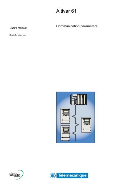
<strong>Altivar</strong> <strong>61</strong><br />
User's manual<br />
Communication parameters<br />
Retain for future use
Table of Contents<br />
Table of Contents _____________________________________________________________________________________________ 3<br />
Documentation structure________________________________________________________________________________________ 6<br />
Presentation _________________________________________________________________________________________________ 7<br />
Notation ____________________________________________________________________________________________________ 9<br />
Description of parameters ________________________________________________________________________________ 9<br />
Drive terminal displays ___________________________________________________________________________________ 9<br />
Profiles ____________________________________________________________________________________________________ 10<br />
What is a profile? ______________________________________________________________________________________ 10<br />
Functional profiles supported by the <strong>Altivar</strong> <strong>61</strong> _______________________________________________________________ 11<br />
I/O profile __________________________________________________________________________________________________ 12<br />
Definition ____________________________________________________________________________________________ 12<br />
Control word - run on state [2 wire] (2C) ____________________________________________________________________ 14<br />
Control word - run on state [3 wire] (3C) ____________________________________________________________________ 15<br />
Status word (ETA) _____________________________________________________________________________________ 16<br />
DSP402 profile ______________________________________________________________________________________________ 17<br />
Functional description __________________________________________________________________________________ 17<br />
DSP402 state chart ____________________________________________________________________________________ 18<br />
Description of states ___________________________________________________________________________________ 19<br />
Control word (CMD) ____________________________________________________________________________________ 21<br />
Status word (ETA) _____________________________________________________________________________________ 23<br />
Starting sequence _____________________________________________________________________________________ 24<br />
Sequence for a drive powered by the power section line supply __________________________________________________ 25<br />
Sequence for a drive with separate control section ____________________________________________________________ 27<br />
Sequence for a drive with line contactor control ______________________________________________________________ 30<br />
Command/reference switching __________________________________________________________________________________ 33<br />
Channels ____________________________________________________________________________________________ 33<br />
Not separate mode ____________________________________________________________________________________ 34<br />
Separate mode _______________________________________________________________________________________ 34<br />
Switching in not separate mode ___________________________________________________________________________ 35<br />
Switching in separate mode ______________________________________________________________________________ 35<br />
Channel switching _____________________________________________________________________________________ 36<br />
Reference switching principle ____________________________________________________________________________ 38<br />
Command switching principle ____________________________________________________________________________ 39<br />
Assigning control word bits ______________________________________________________________________________ 40<br />
Copy on switching _____________________________________________________________________________________ 43<br />
Forced local mode ___________________________________________________________________________________________ 44<br />
Definition ____________________________________________________________________________________________ 44<br />
Forced local mode and reference switching _________________________________________________________________ 45<br />
Forced local mode and command switching _________________________________________________________________ 46<br />
Priority stops________________________________________________________________________________________________ 48<br />
Priority stops on the graphic display terminal ________________________________________________________________ 48<br />
I/O profile ____________________________________________________________________________________________ 48<br />
DSP402 profile ________________________________________________________________________________________ 49<br />
Communication monitoring_____________________________________________________________________________________ 50<br />
Principle _____________________________________________________________________________________________ 50<br />
Network monitoring criteria ______________________________________________________________________________ 50<br />
Detailed operation _____________________________________________________________________________________ 51<br />
Reaction to a communication fault _________________________________________________________________________ 54<br />
Assignment of setpoints from a network___________________________________________________________________________ 55<br />
Setpoint parameters ___________________________________________________________________________________ 55<br />
Without PID regulator __________________________________________________________________________________ 56<br />
With PID regulator _____________________________________________________________________________________ 57<br />
Configuration saving and switching ______________________________________________________________________________ 58<br />
Saving the configuration ________________________________________________________________________________ 58<br />
Restore configuration ___________________________________________________________________________________ 60<br />
Configuration switching via control word ____________________________________________________________________ <strong>61</strong><br />
Configuration switching by selection _______________________________________________________________________ 64<br />
Parameter set switching _______________________________________________________________________________________ 66<br />
Control parameters___________________________________________________________________________________________ 70<br />
Setpoint parameters __________________________________________________________________________________________ 73<br />
Status parameters ___________________________________________________________________________________________ 74<br />
Output value parameters ______________________________________________________________________________________ 82<br />
Output values (speed) __________________________________________________________________________________ 82<br />
Output values (torque) __________________________________________________________________________________ 82<br />
Output values (motor) __________________________________________________________________________________ 83<br />
Reference parameters ________________________________________________________________________________________ 84<br />
References (speed) ____________________________________________________________________________________ 84<br />
Reference (regulator) ___________________________________________________________________________________ 85<br />
3
Table of Contents<br />
Measurement parameters______________________________________________________________________________________ 86<br />
Input measurements ___________________________________________________________________________________ 86<br />
Thermal states ________________________________________________________________________________________ 86<br />
Time ________________________________________________________________________________________________ 86<br />
I/O parameters ______________________________________________________________________________________________ 89<br />
Fault parameters_____________________________________________________________________________________________ 93<br />
Log parameters______________________________________________________________________________________________ 99<br />
Identification parameters _____________________________________________________________________________________ 118<br />
Communication parameters ___________________________________________________________________________________ 120<br />
"Controller Inside" parameters _________________________________________________________________________________ 125<br />
DSP402 standard configuration and adjustment parameters__________________________________________________________ 134<br />
ODVA standard configuration and adjustment parameters ___________________________________________________________ 137<br />
[1.1 SIMPLY START] (SIM-)___________________________________________________________________________________ 138<br />
[1.3 SETTINGS] (SEt-) _______________________________________________________________________________________ 139<br />
[1.4 MOTOR CONTROL] (drC-) ________________________________________________________________________________ 142<br />
[1.5 INPUTS / OUTPUTS CFG] (I-O-) ___________________________________________________________________________ 157<br />
[LI1 CONFIGURATION] (LI-) ____________________________________________________________________________ 158<br />
[LIx CONFIGURATION] (L--) ____________________________________________________________________________ 158<br />
[AI1 CONFIGURATION] (AI1-) __________________________________________________________________________ 160<br />
[AI2 CONFIGURATION] (AI2-) __________________________________________________________________________ 1<strong>61</strong><br />
[AI3 CONFIGURATION] (AI3-) __________________________________________________________________________ 163<br />
[AI4 CONFIGURATION] (AI4-) __________________________________________________________________________ 165<br />
[RP CONFIGURATION] (PLI-) ___________________________________________________________________________ 167<br />
[R1 CONFIGURATION] (RI-) ____________________________________________________________________________ 168<br />
[R2 CONFIGURATION] (R2-) ___________________________________________________________________________ 170<br />
[R3 CONFIGURATION] (r3-) ____________________________________________________________________________ 171<br />
[R4 CONFIGURATION] (r4-) ____________________________________________________________________________ 172<br />
[LO1 CONFIGURATION] (LO1-) _________________________________________________________________________ 173<br />
[LO2 CONFIGURATION] (LO2-) _________________________________________________________________________ 174<br />
[LO3 CONFIGURATION] (LO3-) _________________________________________________________________________ 175<br />
[LO4 CONFIGURATION] (LO4-) _________________________________________________________________________ 176<br />
[AO1 CONFIGURATION] (AO1-) _________________________________________________________________________ 177<br />
[AO2 CONFIGURATION] (AO2-) _________________________________________________________________________ 179<br />
[AO3 CONFIGURATION] (AO3-) _________________________________________________________________________ 180<br />
[1.6 COMMAND] (CtL-)_______________________________________________________________________________________ 181<br />
Assignment conditions for logic inputs and control bits ________________________________________________________ 181<br />
[1.7 APPLICATION FUNCT.] (FUn-) ____________________________________________________________________________ 187<br />
[REFERENCE SWITCH.] (rEF-) _________________________________________________________________________ 187<br />
[REF. OPERATIONS] (OAI-) ____________________________________________________________________________ 188<br />
[RAMP] (rPt-) ________________________________________________________________________________________ 190<br />
[STOP CONFIGURATION] (Stt-) _________________________________________________________________________ 194<br />
[AUTO DC INJECTION] (AdC-) __________________________________________________________________________ 197<br />
[JOG] (JOG-) ________________________________________________________________________________________ 198<br />
[PRESET SPEEDS] (PSS-) _____________________________________________________________________________ 199<br />
[+/- SPEED] (UPd-) ___________________________________________________________________________________ 202<br />
[+/-SPEED AROUND REF.] (SrE-) _______________________________________________________________________ 203<br />
[MEMO REFERENCE] (SPM-) __________________________________________________________________________ 205<br />
[FLUXING BY LI] (FLI-) ________________________________________________________________________________ 206<br />
[PID REGULATOR] (PId-) ______________________________________________________________________________ 207<br />
[PID PRESET REFERENCES] (PRI-) _____________________________________________________________________ 213<br />
[TORQUE LIMITATION] (tOL-) __________________________________________________________________________ 215<br />
[2nd CURRENT LIMIT.] (CLI-) ___________________________________________________________________________ 217<br />
[LINE CONTACTOR COMMAND] (LLC-) __________________________________________________________________ 218<br />
[OUTPUT CONTACTOR CMD] (OCC-) ___________________________________________________________________ 219<br />
[PARAM. SET SWITCHING] (MLP-) ______________________________________________________________________ 221<br />
[MULTIMOTORS/CONFIG.] (MMC-) ______________________________________________________________________ 222<br />
[AUTO TUNING BY LI] (tnL-) ____________________________________________________________________________ 224<br />
[1.8 FAULT MANAGEMENT] (FLt-) _____________________________________________________________________________ 226<br />
[PTC MANAGEMENT] (PtC-) ___________________________________________________________________________ 226<br />
[FAULT RESET] (rSt-) _________________________________________________________________________________ 227<br />
[AUTOMATIC RESTART] (Atr-) __________________________________________________________________________ 228<br />
[CATCH ON THE FLY] (FLr-) ___________________________________________________________________________ 229<br />
[MOTOR THERMAL PROT.] (tHt-) _______________________________________________________________________ 230<br />
[OUTPUT PHASE LOSS] (OPL-) ________________________________________________________________________ 232<br />
[INPUT PHASE LOSS] (IPL-) ___________________________________________________________________________ 232<br />
[DRIVE OVERHEAT] (OHL-) ____________________________________________________________________________ 233<br />
[THERMAL ALARM STOP] (SAt-) ________________________________________________________________________ 234<br />
[EXTERNAL FAULT] (EtF-) _____________________________________________________________________________ 235<br />
4
Table of Contents<br />
[UNDERVOLTAGE MGT] (USb-) ________________________________________________________________________ 236<br />
[IGBT TESTS] (tIt-) ___________________________________________________________________________________ 238<br />
[4-20mA LOSS] (LFL-) _________________________________________________________________________________ 239<br />
[FAULT INHIBITION] (InH-) _____________________________________________________________________________ 240<br />
[COM. FAULT MANAGEMENT] (CLL-) ____________________________________________________________________ 241<br />
[TORQUE OR I LIM. DETECT.] (tId-) _____________________________________________________________________ 242<br />
[DB RES. PROTECTION] (brP-) _________________________________________________________________________ 243<br />
[AUTO-TUNING FAULT] (tnF-) __________________________________________________________________________ 244<br />
[CARDS PAIRING] (PPI-) ______________________________________________________________________________ 244<br />
[FALLBACK SPEED] (LFF-) ____________________________________________________________________________ 244<br />
[RAMP DIVIDER] (FSt-) ________________________________________________________________________________ 245<br />
[DC INJECTION] (dCI-)) _______________________________________________________________________________ 246<br />
Index of parameter names ____________________________________________________________________________________ 247<br />
Index of parameter codes_____________________________________________________________________________________ 271<br />
Index of parameter logic addresses _____________________________________________________________________________ 295<br />
Index of parameter CANopen addresses _________________________________________________________________________ 319<br />
Index of parameter INTERBUS addresses________________________________________________________________________ 342<br />
Index of parameter DeviceNet addresses ________________________________________________________________________ 366<br />
5
Documentation structure<br />
Installation manual<br />
This manual describes:<br />
• How to assemble the drive<br />
• How to connect the drive<br />
Programming manual<br />
This manual describes:<br />
• The functions<br />
• The parameters<br />
• How to use the drive display terminal (integrated display terminal and graphic display terminal)<br />
Communication Parameters Manual<br />
This manual describes:<br />
• The drive parameters with specific information for use via a bus or communication network<br />
• The operating modes specific to communication (state chart)<br />
• The interaction between communication and local control<br />
Modbus, CANopen, Ethernet, Profibus, INTERBUS, Uni-Telway, FIPIO Modbus Plus, and DeviceNet<br />
manuals<br />
These manuals describe:<br />
• Assembly<br />
• Connection to the bus or network<br />
• Diagnostics<br />
• Configuration of the communication-specific parameters via the integrated display terminal or the graphic display terminal<br />
They describe the protocol communication services in detail.<br />
<strong>Altivar</strong> 58/58F migration manual<br />
This manual describes the differences between the <strong>Altivar</strong> <strong>61</strong> and the <strong>Altivar</strong> 58/58F.<br />
It explains how to replace an <strong>Altivar</strong> 58 or 58F, including how to replace drives communicating on a bus or network.<br />
6
Presentation<br />
Magelis XBT<br />
Premium<br />
The <strong>Altivar</strong> <strong>61</strong> drive has been designed to meet all the configuration requirements<br />
encountered within the context of industrial communication installations.<br />
It includes the Modbus and CANopen communication protocols as standard.<br />
FTM<br />
FTM<br />
ATV 31<br />
ATV <strong>61</strong><br />
Sensors<br />
Sensors<br />
Example of configuration on CANopen bus<br />
Two integrated communication ports enable direct access to the Modbus protocol:<br />
• One RJ45 Modbus connector port 2 , located on the drive front panel,<br />
which is used to connect:<br />
• The remote graphic display terminal<br />
• A Magelis industrial HMI terminal<br />
• The PowerSuite software workshop<br />
• One RJ45 Modbus network port 1 , located on the drive’s control terminals,<br />
which is dedicated to control and signaling by a PLC or other type of controller.<br />
It can also be used to connect a display terminal or the PowerSuite software<br />
workshop.<br />
The CANopen protocol can be accessed from the Modbus network port via the<br />
CANopen adapter 3 (1).<br />
The <strong>Altivar</strong> <strong>61</strong> can also be connected to other networks and industrial communication<br />
buses by using one of the communication option cards:<br />
• Ethernet TCP/IP<br />
• Modbus/Uni-Telway. This card provides access to additional functions, which<br />
complement those of the integrated ports: Modbus ASCII and 4-wire RS 485<br />
• Fipio<br />
• Modbus Plus<br />
• Profibus DP<br />
• DeviceNet<br />
• INTERBUS<br />
2<br />
1<br />
3<br />
The control section can be powered separately, thus allowing communication<br />
(monitoring, diagnostics) to be maintained even if the power supply section fails.<br />
The main communication functions of the <strong>Altivar</strong> 58 and <strong>Altivar</strong> 58F drives are<br />
compatible with the <strong>Altivar</strong> <strong>61</strong> (2):<br />
- Connection<br />
- Communication services<br />
- Drive behavior (profile)<br />
- Control and monitoring parameters<br />
- Basic adjustment parameters<br />
The PowerSuite software workshop supports the transfer of configurations from<br />
<strong>Altivar</strong> 58 and <strong>Altivar</strong> 58F drives to the <strong>Altivar</strong> <strong>61</strong>.<br />
(1) If the CANopen adapter is installed, Modbus will not be available on the network port 1 .<br />
(2) Please refer to the ATV 58(F)/ATV <strong>61</strong> migration manual supplied on the documentation CD-ROM.<br />
7
Presentation<br />
All the drive functions are accessible via the network:<br />
• Control<br />
• Monitoring<br />
• Adjustment<br />
• Configuration<br />
If the "Controller Inside" programmable card is installed on the drive, its variables (%MW, etc.) can be accessed via the integrated Modbus<br />
ports or the Ethernet option card.<br />
The speed/torque command and reference can come from different control sources:<br />
• The I/O terminals<br />
• The communication network<br />
• The "Controller Inside" programmable card<br />
• The remote graphic display terminal<br />
• The PowerSuite software workshop (for commissioning and maintenance)<br />
The advanced functions of the <strong>Altivar</strong> <strong>61</strong> enable the switching of these drive control sources to be managed in accordance with application<br />
requirements.<br />
The assignment of periodic communication variables can be selected via:<br />
• The network configuration software (Sycon, etc.)<br />
• The <strong>Altivar</strong> <strong>61</strong>’s communication scanner function<br />
With the exception of DeviceNet, regardless of network type, the <strong>Altivar</strong> <strong>61</strong> can be controlled:<br />
• In accordance with the Drivecom profile (CANopen CiA DSP 402)<br />
• In accordance with the I/O profile, whereby control is as straightforward and flexible as control via the I/O terminals<br />
The DeviceNet card supports the ODVA standard profile.<br />
Communication is monitored on the basis of criteria that are specific to each protocol. Regardless of protocol type, the reaction of the drive<br />
to a communication fault can be configured:<br />
• Drive fault involving: freewheel stop, stop on ramp, fast stop or braked stop<br />
• Stop without drive fault<br />
• Maintain last command received<br />
• Fallback position at preset speed<br />
• Ignore fault<br />
A commands from the CANopen bus is handled with the same priority as an input from the drive terminals. This enables very good response<br />
times to be achieved on the network port via the CANopen adapter.<br />
8
Notation<br />
Description of parameters<br />
Identification<br />
A parameter is described by means of various character strings:<br />
• Code: 4 characters max. The code makes it possible to identify the parameter on the integrated 7-segment display terminal<br />
(Examples: tLIG)<br />
• Name: Description in plain text (used by the PowerSuite software workshop)<br />
• Terminal name: Character string in square brackets for the graphic display terminal [Gen. torque lim]<br />
Addresses<br />
There are 4 formats for specifying parameter addresses:<br />
• Logic address: In decimal and hexadecimal for Modbus, Ethernet TCI/IP, Fipio, Profibus DP protocols<br />
• CANopen index: Index/subindex in hexadecimal<br />
• Interbus-S index: Index/subindex in hexadecimal<br />
• DeviceNet path: Class instance attribute, in hexadecimal<br />
Read/write<br />
• R: Read only<br />
• R/W: Read and write<br />
• R/WS: Read and write, but write only possible when motor is at standstill<br />
Type<br />
• WORD (bit register): Word where each bit represents an item of command, monitoring or configuration information.<br />
• WORD (listing): Word where each value represents an available configuration or a state option.<br />
• INT: Signed integer<br />
• UINT: Unsigned integer<br />
• DINT: Signed double integer<br />
• UDINT: Unsigned double integer<br />
Format<br />
Hexadecimal values are written as follows: 16#pppp.<br />
Drive terminal displays<br />
The menus that appear on the remote graphic display terminal are shown in square brackets.<br />
Example: [1.9 COMMUNICATION].<br />
The menus that appear on the integrated 7-segment display terminal always end with a dash and appear between round brackets.<br />
Example: (COM-).<br />
Parameter names that appear on the remote graphic display terminal are shown in square brackets.<br />
Example: [FALLBACK SPEED].<br />
Parameter codes that appear on the integrated 7-segment display terminal are shown in round brackets.<br />
Example: (LFF).<br />
9
Profiles<br />
What is a profile?<br />
There are 3 types of profile:<br />
• Communication profiles<br />
• Functional profiles<br />
• Application profiles<br />
Communication profiles<br />
A communication profile describes the characteristics of the bus or network:<br />
• Cables<br />
• Connectors<br />
• Electrical characteristics<br />
• Access protocol<br />
• Addressing system<br />
• Periodic exchange service<br />
• Messaging service<br />
• ...<br />
A communication profile is unique to a type of network (Fipio, Profibus DP, etc.) and is used by various different types of device.<br />
Functional profiles<br />
A functional profile describes the behavior of a type of device. It defines:<br />
• The functions<br />
• The parameters (name, format, unit, type, etc.)<br />
• The periodic I/O variables<br />
• State chart(s)<br />
• ...<br />
A functional profile is common to all members of a device family (variable speed drives, encoders, I/O modules, displays, etc.).<br />
Ideally, functional profiles should be network-independent, but in reality they are not. They can feature common or similar parts. As far as<br />
speed drives are concerned, the main profiles are:<br />
• DRIVECOM (INTERBUS)<br />
• DSP402 (CANopen)<br />
• PROFIDRIVE (Profibus)<br />
• ODVA (DeviceNet)<br />
DRIVECOM has been available since 1991.<br />
DSP402 "Device profile for drives and motion control" represents the next stage of this standard’s development and is published by<br />
CanInAutomation.<br />
Application profiles<br />
Application profiles define in their entirety the services to be provided by the devices on a machine. Example: "CiA DSP 417-2 V 1.01 part 2<br />
CANopen application profile for lift control systems - virtual device definitions".<br />
Interchangeability<br />
The aim of communication and functional profiles is to achieve interchangeability of the devices connected via the network.<br />
Although this aim is not always achieved, the profiles facilitate free competition.<br />
10
Profiles<br />
Functional profiles supported by the <strong>Altivar</strong> <strong>61</strong><br />
I/O profile<br />
Using the I/O profile simplifies PLC programming.<br />
The I/O profile is commonly used for control of the terminals and display terminal. It is also supported by the <strong>Altivar</strong> <strong>61</strong> for network control.<br />
The drive starts up as soon as the run command is sent.<br />
The 16 bits of the control word can be assigned to a function or a terminal input.<br />
This profile can be developed for simultaneous control of the drive via:<br />
• The terminals<br />
• The Modbus control word<br />
• The CANopen control word<br />
• The network card control word<br />
• The "Controller Inside" control word<br />
The I/O profile is supported by the drive itself and therefore in turn by all the communication ports (integrated Modbus, CANopen and the<br />
Ethernet, Fipio, ModbusPlus, Modbus, Uni-Telway, Profibus DP, DeviceNet, and INTERBUS communication cards).<br />
DSP402 profile<br />
The drive only starts up following a command sequence.<br />
The control word is standardized.<br />
5 bits of the control word (bits 11 to 15) can be assigned to a function or a terminal input.<br />
The DSP402 profile is supported by the drive itself and therefore in turn by all the communication ports (integrated Modbus, CANopen and<br />
the Ethernet, Fipio, ModbusPlus, Modbus, Uni-Telway, Profibus DP, DeviceNet, and INTERBUS communication cards).<br />
The <strong>Altivar</strong> <strong>61</strong> supports the DSP402 profile’s "Velocity mode".<br />
In DSP402 profile, there are 2 modes that are specific to the <strong>Altivar</strong> <strong>61</strong> and characterize command and reference management<br />
(see section “Command/reference switching”, page 33):<br />
• Separate mode [Separate] (SEP)<br />
• Not separate mode [Not separ.] (SIM)<br />
ODVA (Open DeviceNet Vendor Association) profile<br />
The drive starts up as soon as the run command is sent.<br />
The control word is standardized.<br />
The ODVA profile is supported by the DeviceNet communication card.<br />
11
I/O profile<br />
Definition<br />
The behavior of the drive is identical whether via the network or via the terminals.<br />
The I/O profile is achieved via the following configuration:<br />
Menu Parameter Value<br />
[1.6 - COMMAND] (CtL-) [Profile] (CHCF) [I/O profile] (IO)<br />
As well as to logic inputs of the terminals, drive functions can be assigned to control word bits.<br />
A function input can be assigned to:<br />
• A terminal input (LI2 to LI14)<br />
• A Modbus control word bit (C101 to C115)<br />
• A CANopen control word bit (C201 to C215)<br />
• A network card control word bit (C301 to C315)<br />
• A Controller Inside control word bit (C401 to C415)<br />
• A switched bit (Cd00 to Cd15): See "Command/reference switching" section.<br />
Schematic diagrams:<br />
Fixed assignment on CANopen:<br />
CANopen control word<br />
bit 15<br />
bit 14<br />
bit 13<br />
bit 12<br />
bit 11<br />
bit 10<br />
bit 9<br />
bit 8<br />
bit 7<br />
bit 6<br />
bit 5<br />
bit 4<br />
bit 3<br />
bit 2<br />
bit 1<br />
bit 0<br />
Function<br />
C201<br />
A<br />
C202<br />
B<br />
Fixed assignment to terminals and on CANopen::<br />
CANopen control word<br />
bit 15<br />
bit 14<br />
bit 13<br />
bit 12<br />
bit 11<br />
bit 10<br />
bit 9<br />
bit 8<br />
bit 7<br />
bit 6<br />
bit 5<br />
bit 4<br />
bit 3<br />
bit 2<br />
bit 1<br />
bit 0<br />
Function<br />
C201<br />
A<br />
C202<br />
B<br />
Terminals<br />
LI2<br />
C<br />
LI14<br />
LI13<br />
LI12<br />
LI11<br />
LI10<br />
LI9<br />
LI8<br />
LI7<br />
LI6<br />
LI5<br />
LI4<br />
LI3<br />
LI2<br />
LI1<br />
12
I/O profile<br />
Fixed assignment to terminals on CANopen and on "Controller Inside" card:<br />
CANopen control word<br />
bit 15<br />
bit 14<br />
bit 13<br />
bit 12<br />
bit 11<br />
bit 10<br />
bit 9<br />
bit 8<br />
bit 7<br />
bit 6<br />
bit 5<br />
bit 4<br />
bit 3<br />
bit 2<br />
bit 1<br />
bit 0<br />
Function<br />
C201<br />
A<br />
C202<br />
B<br />
Terminals<br />
LI2<br />
C<br />
C401<br />
bit 15<br />
bit 14<br />
bit 13<br />
bit 12<br />
bit 11<br />
bit 10<br />
bit 9<br />
bit 8<br />
bit 7<br />
bit 6<br />
bit 5<br />
bit 4<br />
bit 3<br />
bit 2<br />
bit 1<br />
bit 0<br />
LI14<br />
LI13<br />
LI12<br />
LI11<br />
LI10<br />
LI9<br />
LI8<br />
LI7<br />
LI6<br />
LI5<br />
LI4<br />
LI3<br />
LI2<br />
LI1<br />
Fast stop<br />
CANopen control word<br />
Stop<br />
Fixed assignment to terminals and on CANopen with command switching :<br />
CANopen control word<br />
bit 15<br />
bit 14<br />
bit 13<br />
bit 12<br />
bit 11<br />
bit 10<br />
bit 9<br />
bit 8<br />
bit 7<br />
bit 6<br />
bit 5<br />
bit 4<br />
bit 3<br />
bit 2<br />
bit 1<br />
bit 0<br />
Function<br />
C201<br />
A<br />
Cd02<br />
B<br />
CANopen<br />
Switching<br />
of command<br />
CCS<br />
Terminals<br />
Terminals<br />
LI14<br />
LI13<br />
LI12<br />
LI11<br />
LI10<br />
LI9<br />
LI8<br />
LI7<br />
LI6<br />
LI5<br />
LI4<br />
LI3<br />
LI2<br />
LI1<br />
LI2<br />
LI5<br />
C<br />
13
I/O profile<br />
Control word - run on state [2 wire] (2C)<br />
Please refer to the [1.5 INPUTS / OUTPUTS CFG] (I-O-) section of the programming manual.<br />
The forward run command is automatically assigned to input LI1 and to bit 0 of the control words.<br />
This assignment cannot be modified.<br />
The run command is active on state 1:<br />
• Of input LI1, if the terminals are active<br />
• Of bit 0 of the control word, if the network is active<br />
Bits 1 to 15 of the control words can be assigned to drive functions.<br />
bit 7 bit 6 bit 5 bit 4 bit 3 bit 2 bit 1 bit 0<br />
Configurable Configurable Configurable Configurable Configurable Configurable Configurable Forward<br />
bit 15 bit 14 bit 13 bit 12 bit 11 bit 10 bit 9 bit 8<br />
Configurable Configurable Configurable Configurable Configurable Configurable Configurable Configurable<br />
In the case of a [2 wire] (2C) run on state command and I/O profile, fixed assignment of a function input is possible using the following<br />
codes:<br />
Bit<br />
Drive terminals<br />
Logic I/O card<br />
Extended I/O<br />
card<br />
Fixed assignments<br />
Modbus CANopen Network card<br />
"Controller Inside"<br />
card<br />
bit 0<br />
Forward<br />
bit 1 LI2 - - C101 C201 C301 C401<br />
bit 2 LI3 - - C102 C202 C302 C402<br />
bit 3 LI4 - - C103 C203 C303 C403<br />
bit 4 LI5 - - C104 C204 C304 C404<br />
bit 5 LI6 - - C105 C205 C305 C405<br />
bit 6 - LI7 - C106 C206 C306 C406<br />
bit 7 - LI8 - C107 C207 C307 C407<br />
bit 8 - LI9 - C108 C208 C308 C408<br />
bit 9 - LI10 - C109 C209 C309 C409<br />
bit 10 - - LI11 C110 C210 C310 C410<br />
bit 11 - - LI12 C111 C211 C311 C411<br />
bit 12 - - LI13 C112 C212 C312 C412<br />
bit 13 - - LI14 C113 C213 C313 C413<br />
bit14 - - - C114 C214 C314 C414<br />
bit15 - - - C115 C215 C315 C415<br />
For example, to assign the operating direction command to bit 1 of CANopen, simply configure the [Reverse assign.] (rrS) parameter with<br />
the value [C201] (C201).<br />
14
I/O profile<br />
Control word - run on state [3 wire] (3C)<br />
Please refer to the [1.5 INPUTS / OUTPUTS CFG] (I-O-).section of the programming manual.<br />
The stop command is automatically assigned to input LI1 and to bit 0 of the control words.<br />
This assignment cannot be modified.<br />
This command enables running on state 1:<br />
• Of input LI1, if the terminals are active<br />
• Of bit 0 of the control word, if the network is active<br />
The forward run command is automatically assigned to input LI2 and to bit 1 of the control words.<br />
This assignment cannot be modified.<br />
The forward run command is active if the stop command is at 1 and on a rising edge (0 V 1):<br />
• Of input LI2, if the terminals are active<br />
• Of bit 1 of the control word, if the network is active<br />
Bits 2 to 15 of the control words can be assigned to drive functions.<br />
bit 7 bit 6 bit 5 bit 4 bit 3 bit 2 bit 1 bit 0<br />
Configurable Configurable Configurable Configurable Configurable Configurable Forward Stop<br />
bit 15 bit 14 bit 13 bit 12 bit 11 bit 10 bit 9 bit 8<br />
Configurable Configurable Configurable Configurable Configurable Configurable Configurable Configurable<br />
In the case of a [3 wire] (3C) run on state command and I/O profile, fixed assignment of a function input is possible using the following<br />
codes:<br />
Bit<br />
Drive terminals<br />
Logic I/O card<br />
Extended I/O<br />
card<br />
Fixed assignments<br />
Modbus CANopen Network card<br />
"Controller Inside"<br />
card<br />
bit 0<br />
Run authorization (Stop)<br />
bit 1<br />
Forward<br />
bit 2 LI3 - - C102 C202 C302 C402<br />
bit 3 LI4 - - C103 C203 C303 C403<br />
bit 4 LI5 - - C104 C204 C304 C404<br />
bit 5 LI6 - - C105 C205 C305 C405<br />
bit 6 - LI7 - C106 C206 C306 C406<br />
bit 7 - LI8 - C107 C207 C307 C407<br />
bit 8 - LI9 - C108 C208 C308 C408<br />
bit 9 - LI10 - C109 C209 C309 C409<br />
bit 10 - - LI11 C110 C210 C310 C410<br />
bit 11 - - LI12 C111 C211 C311 C411<br />
bit 12 - - LI13 C112 C212 C312 C412<br />
bit 13 - - LI14 C113 C213 C313 C413<br />
bit14 - - - C114 C214 C314 C414<br />
bit15 - - - C115 C215 C315 C415<br />
For example, to assign the operating direction command to bit 2 of CANopen, simply configure the [Reverse assign.] (rrS) parameter with<br />
the value [C202] (C202).<br />
15
I/O profile<br />
Status word (ETA)<br />
bit 7 bit 6 bit 5 bit 4 bit 3 bit 2 bit 1 bit 0<br />
Alarm<br />
Reserved<br />
(= 0 or 1)<br />
Reserved (=1) Power present Fault Running Ready<br />
Reserved<br />
(= 0 or 1)<br />
bit 15 bit 14 bit 13 bit 12 bit 11 bit 10 bit 9 bit 8<br />
Direction of<br />
rotation<br />
Stop via STOP<br />
key<br />
Reserved (=0) Reserved (=0)<br />
Reference<br />
outside limits<br />
Reference<br />
reached<br />
Command or<br />
reference via<br />
network<br />
16
DSP402 profile<br />
Functional description<br />
The operation of the drive is encapsulated in 2 main functions, which are illustrated by the 2 diagrams below:<br />
• Control diagram:<br />
Control word<br />
(6040)<br />
State machine<br />
Status word<br />
(6041)<br />
• Simplified diagram, speed reference in "Velocity" mode:<br />
vl_target_velocity<br />
(6042)<br />
Limit<br />
Ramp<br />
vl_velocity_demand<br />
(6043)<br />
Power<br />
module<br />
3<br />
M<br />
vl_velocity_min_max amount (6046)<br />
vl_velocity_acceleration (6048)<br />
vl_velocity_acceleration (6049)<br />
vl_control_effort<br />
(6044)<br />
The main parameters are shown together with their DSP402 name and DSP402/Drivecom index.<br />
These diagrams translate as follows for the <strong>Altivar</strong> system:<br />
Control word<br />
(CMD)<br />
State machine<br />
Status word<br />
(ETA)<br />
Speed reference<br />
(LFRD)<br />
Reference limit<br />
Ramp<br />
Speed reference<br />
after ramp<br />
(FRHD)<br />
Power<br />
module<br />
3<br />
M<br />
Minimum speed (SMIL)<br />
Maximum speed (SMAL)<br />
Acceleration - Speed delta (SPAL)<br />
Acceleration - Time delta (SPAT)<br />
Deceleration - Speed delta (SPDL)<br />
Deceleration - Time delta (SPDT)<br />
Output speed<br />
(RFRD)<br />
17
DSP402 profile<br />
DSP402 state chart<br />
Drive power section line supply not necessarily present<br />
Entry in<br />
state chart<br />
Fault<br />
For all states<br />
13 Fault<br />
Not ready to switch on<br />
Switch on disabled<br />
Fault disappeared<br />
and faults<br />
reset<br />
CMD=16#0080<br />
Fault reaction active<br />
14<br />
Fault<br />
or<br />
Disable<br />
voltage<br />
CMD=16#0000<br />
or<br />
STOP key<br />
or<br />
freewheel<br />
stop<br />
at terminals<br />
Shutdown<br />
CMD=16#0006<br />
or<br />
Ready to switch on<br />
Disable<br />
voltage<br />
CMD=16#0000<br />
or<br />
Quick stop<br />
CMD=16#0002<br />
or<br />
STOP key<br />
Disable<br />
voltage<br />
CMD=16#0000<br />
or<br />
Quick stop<br />
CMD=16#0002<br />
or<br />
STOP key<br />
or<br />
freewheel<br />
stop<br />
at terminals<br />
or<br />
modification<br />
of a configuration<br />
parameter<br />
Disable<br />
voltage<br />
CMD=16#0000<br />
or<br />
STOP key<br />
or<br />
freewheel<br />
stop<br />
at terminals<br />
Switch on<br />
CMD=16#0007<br />
Shutdown<br />
CMD=16#0006<br />
Shutdown<br />
CMD=16#0006<br />
Switched on<br />
Enable<br />
operation<br />
CMD=16#xxxF<br />
Enable<br />
operation<br />
CMD=16#xxxF<br />
Operation enabled<br />
Disable<br />
operation<br />
CMD=16#0007<br />
or<br />
fast stop<br />
Quick stop<br />
CMD=16#0002<br />
Quick stop active<br />
Examples:<br />
ETA=16#0637: Stop or forward, speed reached<br />
ETA=16#8637: Stop or reverse, speed reached<br />
ETA=16#0237: Forward, accelerating or decelerating<br />
ETA=16#8237: Reverse, accelerating or decelerating<br />
Drive power section line supply present<br />
Key:<br />
State<br />
Switched on<br />
Value of<br />
status word<br />
AC power<br />
absent<br />
Enable<br />
operation<br />
CMD=16#xxxF<br />
AC power<br />
present<br />
AC power absent<br />
or present<br />
Transition condition<br />
with example of command<br />
State display on<br />
graphic display terminal<br />
18
DSP402 profile<br />
Description of states<br />
Each state represents an internal reaction by the drive.<br />
This chart will change depending on whether the control word is sent (CMD) or an event occurs (a fault, for example).<br />
The drive state can be identified by the value of the status word (ETA).<br />
Not ready to switch on<br />
Initialization starts. This is a transient state invisible to the communication bus.<br />
Switch on disabled<br />
The drive is inactive.<br />
The drive is locked, no power is supplied to the motor.<br />
For a separate control section, it is not necessary to supply AC power to the power section.<br />
For a separate control section with line contactor, the contactor is not controlled.<br />
The configuration and adjustment parameters can be modified.<br />
Ready to switch on<br />
Power section line supply pending.<br />
For a separate control section, it is not necessary to supply AC power to the power section, but the system will expect it in order to change<br />
to "Switch on" state.<br />
For a separate control section with line contactor, the contactor is not controlled.<br />
The drive is locked, no power is supplied to the motor.<br />
The configuration and adjustment parameters can be modified.<br />
Switched on<br />
The drive is supplied with AC power but is stationary.<br />
For a separate control section, the power section line supply must be present.<br />
For a separate control section with line contactor, the contactor is controlled.<br />
The drive is locked, no power is supplied to the motor.<br />
The power stage of the drive is ready to operate, but voltage has not yet been applied to the output.<br />
The adjustment parameters can be modified.<br />
Modifying a configuration parameter (motor stopped) will switch the drive back to the "Switch on disabled" state.<br />
Operation enabled<br />
The drive is running.<br />
For a separate control section, the power section line supply must be present.<br />
For a separate control section with line contactor, the contactor is controlled.<br />
The drive is unlocked, power is supplied to the motor.<br />
The drive functions are activated and voltage is applied to the motor terminals.<br />
However, in the case of an open-loop drive, if the reference is zero or the "Halt" command is applied, no power is supplied to the motor and<br />
no torque is applied.<br />
Auto-tuning (tUn) requires an injection of current into the motor. The drive must therefore be in the "Operation enabled" state for this<br />
command.<br />
The adjustment parameters can be modified.<br />
Modifying a configuration parameter (motor stopped) will switch the drive back to the "Switch on disabled" state.<br />
19
DSP402 profile<br />
Quick stop active<br />
Emergency stop<br />
The drive performs a fast stop, after which restarting will only be possible once the drive has changed to the "Switch on disabled" state.<br />
During fast stop, the drive is unlocked and power is supplied to the motor.<br />
Fault reaction active<br />
Transient state during which the drive performs an action appropriate to the type of fault.<br />
The drive function is activated or deactivated according to the type of reaction configured in the fault management parameters used for fault<br />
management.<br />
Fault<br />
Drive faulty.<br />
The drive is locked, no power is supplied to the motor.<br />
Summary<br />
State<br />
Power section line supply for<br />
separate control section<br />
Power supplied to motor<br />
Modification of configuration<br />
parameters<br />
Not ready to switch on Not required No Yes<br />
Switch on disabled Not required No Yes<br />
Ready to switch on Not required No Yes<br />
Switched on Required No<br />
Yes, return to "2 - Switch on<br />
disabled" state<br />
Operation enabled<br />
Required<br />
Yes, apart from an open-loop<br />
drive with a zero reference or in<br />
the event of a "Halt" command<br />
No<br />
for an open-loop drive.<br />
Quick stop Required Yes, during fast stop No<br />
Fault reaction active<br />
Depends on fault management<br />
configuration<br />
Depends on fault management<br />
configuration<br />
Fault Not required No Yes<br />
-<br />
20
DSP402 profile<br />
Control word (CMD)<br />
bit 7 bit 6 bit 5 bit 4 bit 3 bit 2 bit 1 bit 0<br />
Fault reset<br />
Enable<br />
Switch on<br />
Quick stop Enable voltage<br />
operation<br />
Ack. fault<br />
Reserved (=0) Reserved (=0) Reserved (=0)<br />
Authorization<br />
Emergency<br />
Contactor<br />
Run command<br />
to supply<br />
stop<br />
control<br />
AC power<br />
bit 15 bit 14 bit 13 bit 12 bit 11 bit 10 bit 9 bit 8<br />
By default,<br />
Halt<br />
direction of<br />
Assignable Assignable Assignable Assignable<br />
Reserved (=0) Reserved (=0)<br />
rotation<br />
Halt<br />
command.<br />
Command<br />
Transition<br />
address<br />
Shutdown 2, 6, 8<br />
Final state<br />
3 - Ready to<br />
switch on<br />
bit7 bit3 bit2 bit1 bit0<br />
Fault<br />
reset<br />
Enable<br />
operation<br />
Quick<br />
stop<br />
Enable<br />
voltage<br />
Switch on<br />
Example value<br />
x x 1 1 0 16#0006<br />
Switch on 3 4 - Switched on x x 1 1 1 16#0007<br />
Enable<br />
operation<br />
Disable<br />
operation<br />
Disable voltage 7, 9, 10, 12<br />
Quick stop<br />
x: Value is of no significance for this command.<br />
0 V 1: Command on rising edge.<br />
4<br />
5 - Operation<br />
enabled<br />
x 1 1 1 1 16#000F<br />
5 4 - Switched on x 0 1 1 1 16#0007<br />
11<br />
7, 10<br />
Fault reset 15<br />
2-Switch on<br />
disabled<br />
6 - Quick stop<br />
active<br />
2-Switch on<br />
disabled<br />
2-Switch on<br />
disabled<br />
x x x 0 x 16#0000<br />
x x 0 1 x 16#0002<br />
0 V 1 x x x x 16#0080<br />
21
DSP402 profile<br />
"Halt" command:<br />
The "Halt" command enables movement to be interrupted without having to leave the "5 - Operation enabled" state. The stop is performed<br />
in accordance with the [Type of stop] (Stt) parameter.<br />
In the case of an open-loop drive, if the "Halt" command is active, no power is supplied to the motor and no torque is applied.<br />
In the case of a closed-loop drive, if the "Halt" command is active, power continues to be supplied to the motor and torque is applied during<br />
stopping.<br />
Assigning control word bits<br />
In DSP402 profile, fixed assignment of a function input is possible using the following codes:<br />
Bit Integrated Modbus CANopen Network card "Controller Inside" card<br />
bit 11 C111 C211 C311 C411<br />
bit 12 C112 C212 C312 C412<br />
bit 13 C113 C213 C313 C413<br />
bit 14 C114 C214 C314 C414<br />
bit 15 C115 C215 C315 C415<br />
For example, to assign the DC injection braking to bit 13 of CANopen, simply configure the [DC injection assign.] (dCI) parameter with<br />
the [C213] (C213) value.<br />
Bit 11 is assigned by default to the operating direction command [Reverse assign.] (rrS).<br />
22
DSP402 profile<br />
Status word (ETA)<br />
bit 7 bit 6 bit 5 bit 4 bit 3 bit 2 bit 1 bit 0<br />
Warning<br />
Alarm<br />
Switch on<br />
disabled<br />
Power section<br />
line supply<br />
disabled<br />
Quick stop<br />
Emergency<br />
stop<br />
Voltage<br />
enabled<br />
Power section<br />
line supply<br />
present<br />
Fault<br />
Operation<br />
enabled<br />
Switched on<br />
Fault Running Ready<br />
Ready to<br />
switch on<br />
Power section<br />
line supply<br />
pending<br />
bit 15 bit 14 bit 13 bit 12 bit 11 bit 10 bit 9 bit 8<br />
Direction of<br />
rotation<br />
Stop via<br />
STOP key<br />
Reserved (=0) Reserved (=0)<br />
Internal limit<br />
active<br />
Reference<br />
outside limits<br />
Target<br />
reached<br />
Reference<br />
reached<br />
Remote<br />
Command or<br />
reference via<br />
network<br />
Reserved (=0)<br />
State<br />
1-Not ready to<br />
switch on<br />
2 - Switch on<br />
disabled<br />
3 - Ready to<br />
switch on<br />
bit6 bit5 bit4 bit3 bit2 bit1 bit0 ETA (W3201)<br />
Switch on Quick Voltage<br />
Operation Switched Ready to masked by<br />
Fault<br />
disabled stop enabled<br />
enabled on switch on 16#006F (1)<br />
0 x x 0 0 0 0 -<br />
1 x x 0 0 0 0 16#0040<br />
0 1 x 0 0 0 1 16#0021<br />
4 - Switched on 0 1 1 0 0 1 1 16#0023<br />
5 - Operation<br />
enabled<br />
6 - Quick stop<br />
active<br />
7 - Fault reaction<br />
active<br />
x: In this state, the value of the bit can be 0 or 1.<br />
0 1 1 0 1 1 1 16#0027<br />
0 0 1 0 1 1 1 16#0007<br />
0 x x 1 1 1 1 -<br />
8 -Fault 0 x x 1 0 0 0<br />
(1) This mask can be used by the PLC program to test the chart state.<br />
16#0008 (2)<br />
or 16#0028<br />
(2) Fault following state "6 - Quick stop active".<br />
23
DSP402 profile<br />
Starting sequence<br />
The command sequence in the state chart depends on how power is being supplied to the drive.<br />
There are three possible scenarios:<br />
Power section<br />
line supply<br />
Control section<br />
power supply<br />
Power section<br />
line supply<br />
Control section<br />
power supply<br />
Power section<br />
line supply<br />
DRIVE DRIVE DRIVE<br />
M M M<br />
Power section<br />
line supply<br />
Direct<br />
Direct<br />
Line contactor<br />
controlled<br />
by the drive<br />
Control section<br />
power supply<br />
Via the power<br />
section<br />
Separate<br />
Separate<br />
24
DSP402 profile<br />
Sequence for a drive powered by the power section line supply<br />
Both the power and control sections are powered by the power section line supply.<br />
If power is supplied to the control section, it has to be supplied to the power section as well.<br />
The following sequence must be applied:<br />
• "2 - Shutdown" command<br />
From all states<br />
Bus or network<br />
Power section<br />
line supply<br />
DRIVE<br />
Disable<br />
9<br />
voltage<br />
1<br />
2<br />
Shutdown<br />
Entry in state machine<br />
3<br />
2<br />
Switch on 3<br />
0<br />
Not ready to<br />
switch on<br />
1<br />
Switch on<br />
disabled<br />
7<br />
Ready to<br />
switch on<br />
Disable voltage<br />
or Quick stop<br />
6 Shutdown<br />
7<br />
8<br />
15<br />
Disable voltage<br />
10<br />
or Quick stop<br />
13<br />
Fault reaction<br />
active<br />
14<br />
Fault<br />
12<br />
Shutdown 8<br />
4<br />
Switched on<br />
M<br />
Enable<br />
operation<br />
4<br />
5<br />
Disable<br />
operation<br />
Operation<br />
5 11 6<br />
enabled<br />
Quick stop<br />
Quick stop<br />
active<br />
25
DSP402 profile<br />
• Check that the drive is in the "3 - Ready to switch on" state.<br />
• Then send the "4 - Enable operation" command.<br />
• The motor can be controlled (send a reference not equal to zero).<br />
From all states<br />
Bus or network<br />
Power section<br />
line supply<br />
DRIVE<br />
Disable<br />
9<br />
voltage<br />
Entry in state machine<br />
1<br />
2<br />
Switch on 2<br />
3<br />
Switch on 3<br />
0<br />
Not ready to<br />
switch on<br />
1<br />
Switch on<br />
disabled<br />
7<br />
Ready to<br />
switch on<br />
Disable voltage<br />
or Quick stop<br />
6 Shutdown<br />
7<br />
8<br />
15<br />
Disable voltage<br />
10<br />
or Quick stop<br />
13<br />
Fault reaction<br />
active<br />
14<br />
Fault<br />
12<br />
M<br />
Shutdown 8<br />
4<br />
Enable<br />
operation<br />
Switched on<br />
4<br />
5<br />
Disable<br />
operation<br />
Operation<br />
5 11 6<br />
enabled<br />
Quick stop<br />
Quick stop<br />
active<br />
26
DSP402 profile<br />
Sequence for a drive with separate control section<br />
Power is supplied separately to the power and control sections.<br />
If power is supplied to the control section, it does not have to be supplied to the power section as well.<br />
The following sequence must be applied:<br />
• The power section line supply is not necessarily present.<br />
• "2 - Shutdown" command<br />
From all states<br />
Bus or network<br />
Control section<br />
power supply<br />
Power section<br />
line supply<br />
DRIVE<br />
Disable<br />
9<br />
voltage<br />
1<br />
2<br />
Shutdown<br />
Entry in state machine<br />
3<br />
2<br />
Switch on 3<br />
0<br />
Not ready to<br />
switch on<br />
1<br />
Switch on<br />
disabled<br />
7<br />
Ready to<br />
switch on<br />
Disable voltage<br />
or Quick stop<br />
6 Shutdown<br />
7<br />
8<br />
15<br />
Disable voltage<br />
10<br />
or Quick stop<br />
13<br />
Fault reaction<br />
active<br />
14<br />
Fault<br />
12<br />
Shutdown 8<br />
4<br />
Switched on<br />
M<br />
Enable<br />
operation<br />
4<br />
5<br />
Disable<br />
operation<br />
Operation<br />
5<br />
enabled<br />
11 6<br />
Quick stop<br />
Quick stop<br />
active<br />
27
DSP402 profile<br />
• Check that the drive is in the "3 - Ready to switch on" state.<br />
• Check that the power section line supply is present ("Voltage enabled" of the status word).<br />
Power section<br />
line supply<br />
• Send the "3 - Switch on" command<br />
Terminal display<br />
Status word<br />
Absent nLP 16#pp21<br />
Present rdY 16#pp31<br />
From all states<br />
Bus or network<br />
Control section<br />
power supply<br />
Power section<br />
line supply<br />
DRIVE<br />
9<br />
Disable<br />
voltage<br />
1<br />
2<br />
Shutdown 2<br />
3<br />
Switch on<br />
Entry in state machine<br />
3<br />
0<br />
Not ready to<br />
switch on<br />
1<br />
Switch on<br />
disabled<br />
7<br />
Ready to<br />
switch on<br />
Disable voltage<br />
or Quick stop<br />
6 Shutdown<br />
7<br />
8<br />
15<br />
Disable voltage<br />
10<br />
or Quick stop<br />
13<br />
Fault reaction<br />
active<br />
14<br />
Fault<br />
12<br />
Shutdown 8<br />
4<br />
Switched on<br />
M<br />
Enable<br />
4 Disable<br />
operation 5<br />
operation<br />
Operation<br />
5<br />
enabled<br />
11 6<br />
Quick stop<br />
Quick stop<br />
active<br />
28
DSP402 profile<br />
• Check that the drive is in the "4 - Switched on" state.<br />
• Then send the "4 - Enable operation" command.<br />
• The motor can be controlled (send a reference not equal to zero).<br />
• If the power section line supply is still not present in the "4 - Switched on" state after a time delay [Mains V. time out] (LCt), the drive will<br />
switch to fault mode (LCF).<br />
From all states<br />
Bus or network<br />
Control section<br />
power supply<br />
Power section<br />
line supply<br />
DRIVE<br />
Disable<br />
9<br />
voltage<br />
Entry in state machine<br />
1<br />
2<br />
Shutdown 2<br />
3<br />
Switch on 3<br />
0<br />
Not ready to<br />
switch on<br />
1<br />
Switch on<br />
disabled<br />
7<br />
Ready to<br />
switch on<br />
Disable voltage<br />
or Quick stop<br />
6 Shutdown<br />
7<br />
8<br />
15<br />
Disable voltage<br />
10<br />
or Quick stop<br />
13<br />
Fault reaction<br />
active<br />
14<br />
Fault<br />
12<br />
M<br />
Shutdown 8<br />
4<br />
Enable<br />
operation<br />
Switched on<br />
4<br />
5<br />
Disable<br />
operation<br />
Operation<br />
5<br />
enabled<br />
11 6<br />
Quick stop<br />
Quick stop<br />
active<br />
29
DSP402 profile<br />
Sequence for a drive with line contactor control<br />
Power is supplied separately to the power and control sections.<br />
If power is supplied to the control section, it does not have to be supplied to the power section as well. The drive controls the line contactor.<br />
The following sequence must be applied:<br />
• The power section line supply is not present as the line contactor is not being controlled.<br />
• Send the "2 - Shutdown" command<br />
From all states<br />
Bus or network<br />
Control section<br />
power supply<br />
DRIVE<br />
Power section<br />
line supply<br />
Disable<br />
9<br />
voltage<br />
1<br />
2<br />
Shutdown<br />
Entry in state machine<br />
3<br />
2<br />
Switch on 3<br />
0<br />
Not ready to<br />
switch on<br />
1<br />
Switch on<br />
disabled<br />
7<br />
Ready to<br />
switch on<br />
Disable voltage<br />
or Quick stop<br />
6 Shutdown<br />
7<br />
8<br />
15<br />
Disable voltage<br />
10<br />
or Quick stop<br />
13<br />
Fault reaction<br />
active<br />
14<br />
Fault<br />
12<br />
Shutdown 8<br />
4<br />
Switched on<br />
M<br />
Enable<br />
4 Disable<br />
operation 5<br />
operation<br />
Operation<br />
5 11 6<br />
enabled<br />
Quick stop<br />
Quick stop<br />
active<br />
30
DSP402 profile<br />
• Check that the drive is in the "3 - Ready to switch on" state<br />
• Send the "3 - Switch on" command, which will close the line contactor and switch on the power section line supply.<br />
From all states<br />
Bus or network<br />
Control section<br />
power supply<br />
DRIVE<br />
Power section<br />
line supply<br />
9 Disable<br />
voltage<br />
Entry in state machine<br />
1<br />
2<br />
Shutdown 2<br />
3<br />
Switch on<br />
3<br />
0<br />
Not ready to<br />
switch on<br />
1<br />
Switch on<br />
disabled<br />
7<br />
Ready to<br />
switch on<br />
Disable voltage<br />
or Quick stop<br />
6 Shutdown<br />
7<br />
8<br />
15<br />
Disable voltage<br />
10<br />
or Quick stop<br />
13<br />
Fault reaction<br />
active<br />
14<br />
Fault<br />
12<br />
Shutdown 8<br />
4<br />
Switched on<br />
M<br />
Enable<br />
operation<br />
4<br />
5<br />
Disable<br />
operation<br />
Operation<br />
5 11 6<br />
enabled<br />
Quick stop<br />
Quick stop<br />
active<br />
31
DSP402 profile<br />
• Check that the drive is in the "4 - Switched on" state<br />
• Then send the "4 - Enable operation" command.<br />
• The motor can be controlled (send a reference not equal to zero).<br />
• If the power section line supply is still not present in the "4 - Switched on" state after a time delay [Mains V. time out] (LCt), the drive will<br />
switch to fault mode (LCF).<br />
From all states<br />
Bus or network<br />
Control section<br />
power supply<br />
DRIVE<br />
Power section<br />
line supply<br />
9<br />
Disable<br />
voltage<br />
Entry in state machine<br />
1<br />
2<br />
Shutdown 2<br />
3<br />
Switch on 3<br />
0<br />
Not ready to<br />
switch on<br />
1<br />
Switch on<br />
disabled<br />
7<br />
Ready to<br />
switch on<br />
Disable voltage<br />
or Quick stop<br />
6 Shutdown<br />
7<br />
8<br />
15<br />
Disable voltage<br />
10<br />
or Quick stop<br />
13<br />
Fault reaction<br />
active<br />
14<br />
Fault<br />
12<br />
M<br />
Shutdown 8<br />
4<br />
Enable<br />
operation<br />
Switched on<br />
4<br />
5<br />
Disable<br />
operation<br />
Operation<br />
5 11 6<br />
enabled<br />
Quick stop<br />
Quick stop<br />
active<br />
32
Command/reference switching<br />
Channels<br />
The 6 <strong>Altivar</strong> <strong>61</strong> channels are:<br />
• The terminals<br />
• The graphic display terminal<br />
• The integrated Modbus ports<br />
• The integrated CANopen port<br />
• The network card<br />
• The Controller Inside card<br />
The <strong>Altivar</strong> <strong>61</strong> has 2 integrated Modbus ports. These 2 ports are physically independent of one another but together constitute a single logic<br />
channel.<br />
The drive does not distinguish between commands and references that come from the Modbus network port and those that come from the<br />
Modbus HMI port.<br />
With the <strong>Altivar</strong> drive, the command and reference source can be selected together or separately:<br />
• Via configuration<br />
• Via switching at the terminals or via a bus or communication network<br />
Channel commands and references<br />
All the drive’s command and reference parameters are managed on a channel-by-channel basis.<br />
It is possible to identify the last value written for each channel and each command or reference parameter:<br />
Parameter name<br />
Taken into<br />
account by the<br />
drive<br />
Modbus<br />
Parameter code<br />
CANopen<br />
Communication<br />
card<br />
Controller<br />
Inside<br />
Control word CMd CMd1 CMd2 CMd3 CMd4<br />
Extended control word CMI CMI1 CMI2 CMI3 CMI4<br />
Speed reference (rpm) LFrd LFrd1 LFrd2 LFrd3 LFrd4<br />
Frequency reference (0.1 Hz) LFr LFr1 LFr2 LFr3 LFr4<br />
PI regulator reference PISP PIr1 PIr2 PIr3 PIr4<br />
Analog multiplier reference MFr MFr1 MFr2 MFr3 MFr4<br />
33
Command/reference switching<br />
Not separate mode<br />
Command and reference come from the same channel.<br />
-10 V<br />
+10 V<br />
TERMINALS<br />
Reference<br />
Command<br />
In DSP402 profile, not separate mode is configured via the terminal:<br />
Menu Parameter Value<br />
[1.6 - COMMAND] (CtL-) [Profile] (CHCF) [Not separ.] (SIM)<br />
Separate mode<br />
Command and reference may come from different channels.<br />
CANopen<br />
Digital<br />
reference<br />
CANopen<br />
TERMINALS<br />
Command<br />
Reference<br />
In DSP402 profile, the separate mode is achieved via configuration with the terminal:<br />
Menu Parameter Value<br />
[1.6 - COMMAND] (CtL-) [Profile] (CHCF) [Separate] (SEP)<br />
In I/O profile, the drive is automatically in separate mode.<br />
Menu Parameter Value<br />
[1.6 - COMMAND] (CtL-) [Profile] (CHCF) [I/O profile] (IO)<br />
34
Command/reference switching<br />
Switching in not separate mode<br />
Switching takes place between 2 channels simultaneously for both reference and command.<br />
CANopen<br />
Control register<br />
Digital reference<br />
CANopen<br />
-10V<br />
+10v<br />
TERMINALS<br />
Reference<br />
Command<br />
In this example, either CANopen or the terminals supply both command and reference.<br />
Switching in separate mode<br />
Switching can take place between 2 channels separately for reference and command.<br />
CANopen<br />
Digital reference<br />
CANopen<br />
-10 V<br />
+10 V<br />
TERMINALS<br />
Reference<br />
Command<br />
In this example, the command always comes from the terminals; the reference can come either from CANopen or from the terminals.<br />
35
Command/reference switching<br />
Channel switching<br />
Reference channel configuration<br />
Reference channel configuration enables reference sources to be predefined, which can be modified or switched subsequently via a<br />
command.<br />
There are 3 predefined reference channels:<br />
• Reference channel 1<br />
• Reference channel 1B<br />
• Reference channel 2<br />
Reference channels 1 and 1B are used for drive application functions.<br />
Reference channel 2 is connected directly to the reference limiting function, bypassing the application functions.<br />
The predefined reference channels are assigned via the [Ref. 1 channel] (Fr1), [Ref. 1B channel] (Fr1b) and [Ref. 2 channel] (Fr2)<br />
configuration parameters, which can have the following values:<br />
• [No] (nO): Not assigned<br />
• [AI1 ref.] (AI1): Analog input AI1<br />
• [AI2 ref.] (AI2): Analog input AI2<br />
• [AI3 ref.] (AI3): Analog input AI3 (if extension card present)<br />
• [AI4 ref.] (AI4): Analog input AI4 (if extension card present)<br />
• [Pulse Input] (PI): Frequency input (if card present)<br />
• [HMI] (LCC): Graphic display terminal<br />
• [Modbus] (Mdb): Integrated Modbus<br />
• [CANopen] (CAn): Integrated CANopen<br />
• [Com. card] (nEt): Communication card (if present)<br />
• [Prog. card] (APP): Controller Inside card (if present).<br />
• [Encoder] (PG): Encoder input (if card present)<br />
Note: The "+speed/-speed" function is on reference channel 2. See the programming manual for more information.<br />
Command channel configuration<br />
Command channel configuration enables command sources to be predefined, which can be modified or switched subsequently via a<br />
command.<br />
There are 2 predefined command channels:<br />
• Command channel 1<br />
• Command channel 2<br />
The predefined command channels are assigned via the [Cmd channel 1] (Cd1) and [Cmd channel 2] (Cd2) configuration parameters,<br />
which can have the following values:<br />
• [Terminals] (tEr): Terminals<br />
• [HMI] (LCC): Graphic display terminal<br />
• [Modbus] (Mdb): Integrated Modbus<br />
• [CANopen] (CAn): Integrated CANopen<br />
• [Com. card] (nEt): Communication card (if present)<br />
• [Prog. card] (APP): Controller Inside card (if present).<br />
36
Command/reference switching<br />
Switches<br />
A channel switch is used to select predefined channels.<br />
It can be:<br />
• Defined via configuration<br />
• Actuated either by an input or a network bit<br />
• Written via a network during operation<br />
The possible switch values are:<br />
Switching of<br />
function reference<br />
[Ref 1B switching] (rCb)<br />
The values Fr1, Fr1b, Fr2, Cd1 and Cd2 are either configured or written via the network during operation.<br />
In I/O and DSP402 profiles (separate), independent switching is possible:<br />
In DSP402 profile (not separate), switching is simultaneous:<br />
Switching of<br />
direct reference<br />
[Ref. 2 switching] (rFC)<br />
Command switching<br />
[Cmd switching] (CCS)<br />
Channel 1 Fr1 Fr1 Cd1<br />
Channel 1B Fr1b - -<br />
Channel 2 - Fr2 Cd2<br />
Drive input<br />
Logic I/O card input<br />
Extended I/O card input<br />
Modbus command bit<br />
CANopen command bit<br />
Network command bit<br />
Controller Inside command bit<br />
LI1 ... LI6<br />
LI7 ... LI10<br />
LI11 ... LI14<br />
bit 0 = C100 ... bit 15 = C115<br />
bit 0 = C200 ... bit 15 = C215<br />
bit 0 = C300 ... bit 15 = C315<br />
bit 0 = C400 ... bit 15 = C415<br />
Type Switching Channel 1 Channel 2<br />
Reference<br />
Command<br />
Function reference switching<br />
[Ref 1B switching] (rCb)<br />
Direct reference switching<br />
[Ref. 2 switching] (rFC)<br />
Command switching<br />
[Cmd switching] (CCS)<br />
Function reference 1<br />
[Ref. 1 channel] (Fr1)<br />
Function reference 1 or 1B<br />
[Ref. 1 channel] (Fr1)<br />
[Ref. 1B channel] (Fr1b)<br />
Command 1<br />
[Cmd channel 1] (Cd1)<br />
Type Switching Channel 1 Channel 2<br />
Reference<br />
and<br />
command<br />
Direct reference switching<br />
[Ref. 2 switching] (rFC)<br />
Function reference 1 or 1B<br />
[Ref. 1 channel] (Fr1)<br />
[Ref. 1B channel] (Fr1b)<br />
Command 1<br />
[Cmd channel 1] (Cd1)<br />
Function reference 1B<br />
[Ref. 1B channel] (Fr1b)<br />
Direct reference 2<br />
[Ref. 2 channel] (Fr2)<br />
Command 2<br />
[Cmd channel 2] (Cd2)<br />
Direct reference 2<br />
[Ref. 2 channel] (Fr2)<br />
Command 2<br />
[Cmd channel 2] (Cd1)<br />
37
Command/reference switching<br />
Reference switching principle<br />
A detailed description can be found in the programming manual.<br />
The diagram below shows reference switching as applicable to all modes:<br />
• I/O profile<br />
• DSP402 profile and separate mode<br />
• DSP402 profile and not separate mode<br />
Reference channel 1<br />
Fr1<br />
AI1C<br />
AI1<br />
AI2C<br />
AI2<br />
LFr<br />
Display Terminal terminal<br />
rFD1<br />
rFD2<br />
rFD3<br />
rFD4<br />
Modbus<br />
CANopen<br />
RØseau Network<br />
Controller<br />
Function<br />
reference<br />
switching<br />
rCb<br />
Function<br />
Reference channel 1B<br />
Fr1b<br />
AI1C<br />
AI2C<br />
LFr<br />
rFD1<br />
rFD2<br />
rFD3<br />
AI1<br />
AI2<br />
Display terminal<br />
Modbus<br />
CANopen<br />
Network<br />
Fr1<br />
Fr1b<br />
LI1pp<br />
C1pp<br />
C2pp<br />
C3pp<br />
C4pp<br />
Application<br />
function<br />
output<br />
reference<br />
Direct<br />
reference<br />
switching<br />
rFC<br />
Reference<br />
limit<br />
Ramp<br />
rFD4<br />
Controller<br />
AI1C<br />
AI2C<br />
LFr<br />
rFD1<br />
Reference channel 2<br />
Fr2<br />
AI1<br />
AI2<br />
Display terminal<br />
Modbus<br />
Direct<br />
reference 2<br />
Fr1<br />
Fr2<br />
LIpp<br />
C1pp<br />
C2pp<br />
C3pp<br />
C4pp<br />
rFD2<br />
CANopen<br />
rFD3<br />
Network<br />
rFD4<br />
Controller<br />
38
Command/reference switching<br />
Command switching principle<br />
A detailed description can be found in the programming manual.<br />
I/O profile or DSP402 profile (separate mode)<br />
Command channel 1<br />
Cd1<br />
Terminals<br />
LIx<br />
Display terminal<br />
RUN/STOP Terminal<br />
FWD/REV<br />
CMD1<br />
CMD2<br />
CMD3<br />
CMD4<br />
Modbus<br />
Modbus<br />
CANopen<br />
CANopen<br />
Network<br />
RØseau<br />
Controller<br />
Controller<br />
Command channel 2<br />
Cd2<br />
Terminals<br />
LIx Bornier<br />
Display terminal<br />
RUN/STOP Terminal<br />
FWD/REV<br />
CMD1<br />
Modbus<br />
CANopen<br />
CMD2<br />
Network<br />
CMD3<br />
Controller<br />
CMD4 Controller<br />
Command<br />
switching<br />
CCS<br />
Cd1<br />
Cd2<br />
LIpp<br />
C1pp<br />
C2pp<br />
C3pp<br />
C4pp<br />
Run<br />
Stop<br />
Forward<br />
Reverse<br />
DSP402 profile (not separate mode)<br />
Reference channel 1<br />
Fr1<br />
LIx<br />
RUN/STOP<br />
FWD/REV<br />
CMD1<br />
CMD2<br />
CMD3<br />
CMD4<br />
AI1<br />
AI2<br />
Display terminal<br />
Modbus<br />
CANopen<br />
Network<br />
Controller<br />
Reference channel 2<br />
Fr2<br />
LIx<br />
AI1<br />
AI2<br />
RUN/STOP<br />
FWD/REV<br />
CMD1<br />
CMD2<br />
CMD3<br />
CMD4<br />
Display terminal<br />
Modbus<br />
CANopen<br />
Network<br />
Controller<br />
Direct<br />
reference<br />
switching<br />
rFC<br />
Fr1<br />
Fr2<br />
LIpp<br />
C111 ... C115<br />
C211 ... C215<br />
C311 ... C315<br />
C411 ... C415<br />
Run<br />
Stop<br />
Forward<br />
Reverse<br />
39
Command/reference switching<br />
Assigning control word bits<br />
I/O profile<br />
The I/O profile is extremely flexible in terms of assigning and switching the 16 control word bits.<br />
To switch a control word bit using:<br />
• an input from the terminals<br />
• or a control word bit from another communication channel<br />
simply configure a switched assignment for the function input, instead of a fixed assignment.<br />
Inputs and bits of the same order are switched.<br />
Inputs LI1 to LI6 of the drive terminals can be used to switch control word bits 0 to 5.<br />
With a logic I/O card using inputs LI7 to LI10, control word bits 6 to 9 can also be switched.<br />
With an extended logic I/O card using inputs LI11 to LI14, control word bits 10 to 13 can also be switched.<br />
Once an item has been assigned as switchable, it can no longer be assigned as fixed, and vice versa.<br />
Example: Once a function input has been assigned to CD04, it cannot be assigned to LI5, C104, C204, C304 or C404.<br />
Example<br />
Function input A is always controlled by bit 1 of the CANopen control word.<br />
Function input B is always controlled by input LI5 on the terminals.<br />
Depending on the value of LI2, function input C is controlled:<br />
• Either by input LI3 on the terminals<br />
• Or by bit 2 of the CANopen control word<br />
CANopen control word<br />
bit 15<br />
bit 14<br />
bit 13<br />
bit 12<br />
bit 11<br />
bit 10<br />
bit 9<br />
bit 8<br />
bit 7<br />
bit 6<br />
bit 5<br />
bit 4<br />
bit 3<br />
bit 2<br />
bit 1<br />
bit 0<br />
Function<br />
C201<br />
A<br />
Cd02<br />
C<br />
CANopen<br />
Switching<br />
of command<br />
CCS<br />
Terminals<br />
Terminals<br />
LI14<br />
LI13<br />
LI12<br />
LI11<br />
LI10<br />
LI9<br />
LI8<br />
LI7<br />
LI6<br />
LI5<br />
LI4<br />
LI3<br />
LI2<br />
LI1<br />
LI2<br />
LI5<br />
B<br />
40
Command/reference switching<br />
The tables below show assignments on the basis of input or bit.<br />
Run on state command [2 wire] (2C):<br />
In all macro configurations, bit 1 is assigned by default to the operating direction command [Reverse assign.] (rrS)<br />
Bit<br />
Switched<br />
assignment<br />
Drive<br />
terminals<br />
Logic I/O card<br />
Extended I/O<br />
card<br />
Fixed assignments<br />
Integrated<br />
Modbus<br />
CANopen<br />
Network card<br />
Run on edge command [3 wire] (3C):<br />
In all macro configurations, bit 2 is assigned by default to the operating direction command [Reverse assign.] (rrS)<br />
"Controller<br />
Inside" card<br />
bit 0<br />
Forward<br />
bit 1 Cd01 LI2 - - C101 C201 C301 C401<br />
bit 2 Cd02 LI3 - - C102 C202 C302 C402<br />
bit 3 Cd03 LI4 - - C103 C203 C303 C403<br />
bit 4 Cd04 LI5 - - C104 C204 C304 C404<br />
bit 5 Cd05 LI6 - - C105 C205 C305 C405<br />
bit 6 Cd06 - LI7 - C106 C206 C306 C406<br />
bit 7 Cd07 - LI8 - C107 C207 C307 C407<br />
bit 8 Cd08 - LI9 - C108 C208 C308 C408<br />
bit 9 Cd09 - LI10 - C109 C209 C309 C409<br />
bit 10 Cd10 - - LI11 C110 C210 C310 C410<br />
bit 11 Cd11 - - LI12 C111 C211 C311 C411<br />
bit 12 Cd12 - - LI13 C112 C212 C312 C412<br />
bit 13 Cd13 - - LI14 C113 C213 C313 C413<br />
bit 14 Cd14 - - - C114 C214 C314 C414<br />
bit 15 Cd15 - - - C115 C215 C315 C415<br />
Bit<br />
Switched<br />
assignment<br />
Drive<br />
terminals<br />
Logic I/O card<br />
Extended I/O<br />
card<br />
Fixed assignments<br />
Integrated<br />
Modbus<br />
CANopen<br />
Network card<br />
"Controller<br />
Inside" card<br />
bit 0<br />
Run authorization<br />
bit 1<br />
Forward<br />
bit 2 Cd02 LI3 - - C102 C202 C302 C402<br />
bit 3 Cd03 LI4 - - C103 C203 C303 C403<br />
bit 4 Cd04 LI5 - - C104 C204 C304 C404<br />
bit 5 Cd05 LI6 - - C105 C205 C305 C405<br />
bit 6 Cd06 - LI7 - C106 C206 C306 C406<br />
bit 7 Cd07 - LI8 - C107 C207 C307 C407<br />
bit 8 Cd08 - LI9 - C108 C208 C308 C408<br />
bit 9 Cd09 - LI10 - C109 C209 C309 C409<br />
bit 10 Cd10 - - LI11 C110 C210 C310 C410<br />
bit 11 Cd11 - - LI12 C111 C211 C311 C411<br />
bit 12 Cd12 - - LI13 C112 C212 C312 C412<br />
bit 13 Cd13 - - LI14 C113 C213 C313 C413<br />
bit 14 Cd14 - - - C114 C214 C314 C414<br />
bit 15 Cd15 - - - C115 C215 C315 C415<br />
41
Command/reference switching<br />
DSP402 profile<br />
Control word bits of the same order are switched if the function inputs are assigned to switchable bits.<br />
Switching may be possible using LI12, LI13 or LI14 on an extended I/O card.<br />
Once a bit has been assigned to a switchable assignment, it can no longer be assigned to a fixed assignment, and vice versa.<br />
Example: Once a function input has been assigned to Cd04, it cannot be assigned to LI5, C104, C204, C304 or C404.<br />
The table below shows assignments on the basis of input or bit.<br />
Bit<br />
Switched<br />
assignment<br />
Drive<br />
terminals<br />
Logic I/O card<br />
Extended I/O<br />
card<br />
Fixed assignments<br />
Integrated<br />
Modbus<br />
CANopen<br />
Network card<br />
"Controller<br />
Inside" card<br />
bit 0 - LI1 - - - - - -<br />
bit 1 - LI2 - - - - - -<br />
bit 2 - LI3 - - - - - -<br />
bit 3 - LI4 - - - - - -<br />
bit 4 - LI5 - - - - - -<br />
bit 5 - LI6 - - - - - -<br />
bit 6 - - LI7 - - - - -<br />
bit 7 - - LI8 - - - - -<br />
bit 8 - - LI9 - - - - -<br />
bit 9 - - LI10 - - - - -<br />
bit 10 - - - LI11 - - - -<br />
bit 11 Cd11 - - LI12 C111 C211 C311 C411<br />
bit 12 Cd12 - - LI13 C112 C212 C312 C412<br />
bit 13 Cd13 - - LI14 C113 C213 C313 C413<br />
bit 14 Cd14 - - - C114 C214 C314 C414<br />
bit 15 Cd15 - - - C115 C215 C315 C415<br />
42
Command/reference switching<br />
Copy on switching<br />
When switching channels, it is possible to copy the reference or command from function channel 1 to direct channel 2.<br />
Menu<br />
[1.6 COMMAND] (CtL-)<br />
Submenu<br />
Parameter<br />
[Copy channel 1 --> 2]<br />
Possible values<br />
No copy.<br />
[No] (nO)<br />
Copy reference<br />
[Reference] (SP)<br />
Copy command<br />
[Command] (Cd)<br />
Copy command and reference<br />
[Cmd + ref.] (ALL)<br />
If a copy is not made, the drive stops according to the configured stop type [Type of stop] (Stt) until the first command and reference are<br />
received.<br />
The reference before ramp (FrH) is copied unless the direct channel 2 reference is via +/- speed.<br />
If the direct channel 2 reference is via +/- speed, the after ramp (rFr) reference is copied.<br />
If the direct channel 2 command is via the terminals, the function channel 1 command is not copied even in pulse control (3-wire)<br />
[3 wire] (3C).<br />
If the direct channel 2 reference is via AI1, AI2, AI3, AI4, the encoder input or frequency input, the function channel 1 reference is not copied.<br />
43
Forced local mode<br />
Definition<br />
Forced local mode supports switching to the terminals or display terminal.<br />
This function complements channel switching and makes it possible to make use of an existing function from the <strong>Altivar</strong> 58 range.<br />
Forced local mode is only available in DSP402 profile, not in I/O profile.<br />
All other communication takes priority over forced local mode.<br />
Forced local mode can be configured via the display terminal:<br />
Menu<br />
Submenu<br />
[1.9 COMMUNICATION] (COM-) [FORCED LOCAL] (LCF-)<br />
Parameter<br />
Forced local switch<br />
[Forced local assign.] (FLO)<br />
Forced local channel<br />
[Forced local Ref.] (FLOC)<br />
Possible values<br />
Function inactive:<br />
[No] (nO)<br />
Assignment to a logic input (LI1 ... LI14):<br />
[LI1] (LI1) ... [LI14] (LI14)<br />
Forced local mode is active when the input is at state 1.<br />
Forced local on stop.<br />
[No] (nO)<br />
Assignment of the command to the terminals and of the reference to one of the analog inputs<br />
AI1 ... AI4<br />
[AI2 ref.] (AI2), [AI3 ref.] (AI3), [AI4 ref.] (AI4)<br />
Assignment of the command to the terminals and of the reference to the frequency input (if card<br />
present)<br />
[Pulse Input] (PI)<br />
Assignment of the reference [HMI Frequency ref.] (LFr) and of the command<br />
(RUN/STOP/FWD/REV buttons) to the graphic display terminal<br />
[HMI] (LCC)<br />
In "forced local" state:<br />
• Any attempts to write the parameter via one of these channels is rejected (applies to command, reference and adjustment<br />
parameters).<br />
• However, the parameters can be read.<br />
• The drive does not register a communication fault.<br />
On exiting "forced local" mode:<br />
• The drive copies the run commands, the direction and the forced local reference to the active channel (maintained).<br />
• Monitoring of the active command and reference channels resumes following a time delay [Time-out forc. local] (FLOt).<br />
• Drive control only takes effect once the drive has received the reference and the command.<br />
The time delay [Time-out forc. local] (FLOt) (default value = 10 s) can be configured via the remote graphic display terminal:<br />
Menu Submenu Parameter<br />
[1.9 COMMUNICATION] (COM-) [FORCED LOCAL] (LCF-) [Time-out forc. local] (FLOt)<br />
44
Forced local<br />
Forced local mode and reference switching<br />
A detailed description can be found in the programming manual.<br />
This diagram shows reference switching as applicable to all modes:<br />
• DSP402 profile and separate mode<br />
• DSP402 profile and not separate mode<br />
Reference channel 1<br />
Fr1<br />
AI1C<br />
AI1<br />
AI2C<br />
LFr<br />
AI2<br />
Display terminal<br />
Forced local channel<br />
FLOC<br />
rFD1<br />
rFD2<br />
rFD3<br />
rFD4<br />
Modbus<br />
CANopen<br />
Network<br />
Controller<br />
Function<br />
reference<br />
switching<br />
rCB<br />
Function<br />
AI1C<br />
AI2C<br />
AI3C<br />
AI4C<br />
AI1<br />
AI2<br />
AI3<br />
AI4<br />
Reference channel 1B<br />
Fr1B<br />
LFr<br />
Display terminal<br />
AI1C<br />
AI2C<br />
LFr<br />
rFD1<br />
rFD2<br />
AI1<br />
AI2<br />
Display terminal<br />
Modbus<br />
CANopen<br />
Fr1<br />
Fr1b<br />
LIpp<br />
C111 ... C115<br />
C211 ... C215<br />
C311 ... C315<br />
C411 ... C415<br />
Application<br />
function<br />
output<br />
reference<br />
Direct reference<br />
switching<br />
rFB<br />
Forced<br />
local<br />
switching<br />
FLO<br />
Reference<br />
limit<br />
Ramp<br />
rFD3<br />
Network<br />
rFD4<br />
Controller<br />
AI1C<br />
AI2C<br />
LFr<br />
rFD1<br />
Reference channel 2<br />
Fr2<br />
AI1<br />
AI2<br />
Display terminal<br />
Modbus<br />
Direct<br />
reference 2<br />
Fr1<br />
Fr2<br />
LIpp<br />
C111 ... C115<br />
C211 ... C215<br />
C311 ... C315<br />
C411 ... C415<br />
LI1 ... LI14<br />
rFD2<br />
CANopen<br />
rFD3<br />
Network<br />
rFD4<br />
Controller<br />
45
Forced local<br />
Forced local mode and command switching<br />
A detailed description can be found in the programming manual.<br />
DSP402 profile (separate mode)<br />
Command channel 1<br />
Cd1<br />
LIx<br />
RUN/STOP<br />
FWD/REV<br />
CMD1<br />
CMD2<br />
CMD3<br />
Terminals<br />
Display terminal<br />
Modbus<br />
CANopen<br />
Network<br />
LIx<br />
Forced local channel<br />
FLOC<br />
AI1<br />
AI2<br />
AI3<br />
AI4<br />
CMD4<br />
Controller<br />
RUN/STOP<br />
FWD/REV<br />
Display terminal<br />
LIx<br />
RUN/STOP<br />
FWD/REV<br />
Command channel 2<br />
Cd2<br />
Terminals<br />
Display terminal<br />
Command<br />
switching<br />
CCS<br />
Forced<br />
local<br />
switching<br />
FLO<br />
Run<br />
Stop<br />
Forward<br />
Reverse<br />
CMD1<br />
Modbus<br />
CMD2<br />
CMD3<br />
CMD4<br />
CANopen<br />
Network<br />
Controller<br />
Cd1<br />
Cd2<br />
LIpp<br />
C111 ... C115<br />
C211 ... C215<br />
C311 ... C315<br />
C411 ... C415<br />
LI1 ... LI14<br />
46
Forced local<br />
DSP402 profile (not separate mode)<br />
LIx<br />
Reference channel 1<br />
Fr1<br />
AI1<br />
Forced local channel<br />
FLOC<br />
AI2<br />
LIx<br />
AI1<br />
RUN/STOP<br />
FWD/REV<br />
CMD1<br />
CMD2<br />
Display terminal<br />
Modbus<br />
CANopen<br />
AI2<br />
AI3<br />
AI4<br />
CMD3<br />
CMD4<br />
Network<br />
Controller<br />
RUN/STOP<br />
FWD/REV<br />
Display terminal<br />
LIx<br />
Reference channel 2<br />
Fr2<br />
AI1<br />
AI2<br />
Direct<br />
reference<br />
switching<br />
rFC<br />
Forced<br />
local<br />
switching<br />
FLO<br />
Run<br />
Stop<br />
Forward<br />
Reverse<br />
RUN/STOP<br />
FWD/REV<br />
CMD1<br />
CMD2<br />
CMD3<br />
CMD4<br />
Display terminal<br />
Modbus<br />
CANopen<br />
Network<br />
Controller<br />
Fr1<br />
Fr2<br />
LIpp<br />
C111 ... C115<br />
C211 ... C215<br />
C311 ... C315<br />
C411 ... C415<br />
LI1 ... LI14<br />
47
Priority stops<br />
Priority stops<br />
Priority stops on the graphic display terminal<br />
Even if the graphic display terminal is not the active command channel, pressing the STOP key on the graphic display terminal will trigger<br />
a freewheel stop if:<br />
• the [Stop Key priority] (PSt) parameter has been configured as [Yes] (YES) (factory setting) in the [1.6 - COMMAND] (CtL-) menu, via the<br />
terminal.<br />
If the graphic display terminal is the active command channel, the STOP key will trigger a stop according to the type of stop configured with<br />
the [Type of stop] (Stt) parameter, regardless of the value of the [Stop Key priority] (PSt) parameter.<br />
The role played by the graphic display terminal is independent of the profile.<br />
I/O profile<br />
In the I/O profile:<br />
Stop and fault commands, configured as fixed assignments (LIpp, C1pp, C2pp, C3pp, C4pp) to terminal inputs or control word bits, are<br />
priority commands, even if the channel is not active.<br />
Commands, configured as switched assignments (Cd00 ... Cd15) are active only if the channel is active.<br />
Fixed assignments are configured using the following values:<br />
Channel<br />
Run on state command<br />
[2 wire] (2C)<br />
Run on edge command<br />
[3 wire] (3C)<br />
Drive terminals LI2 ... LI6 LI3 ... LI6<br />
Logic I/O card<br />
LI7 ... LI10<br />
Extended I/O card<br />
LI11 ... LI14<br />
Integrated Modbus C101 ... C115 C102 ... C115<br />
CANopen C201 ... C215 C202 ... C215<br />
Communication card C301 ... C315 C302 ... C315<br />
"Controller Inside" card C401 ... C415 C402 ... C415<br />
Command Configuration = 0 = 1 Value for starting (1)<br />
Freewheel stop [Freewheel stop ass.] (nSt) stop no stop 1<br />
Fast stop [Fast stop assign.] (FSt) stop no stop 1<br />
DC injection braking [DC injection assign.] (dCI) no braking braking 0<br />
External fault [External fault ass.] (EtF) no fault fault 0<br />
(1) If assignment is fixed, value required for starting, even if another channel is active.<br />
In the case of a run on edge command, configured via [3 wire] (3C):<br />
The stop command (run enable) is assigned by default to switched bit order 0 (equivalent to Cd00):<br />
• It is only active on the terminals (LI1) if the terminals are is active.<br />
• It is only active via the network (bit 0) if the network is active.<br />
48
Priority stops<br />
DSP402 profile<br />
In DSP402 profile, separate or not separate mode:<br />
Stop and fault commands configured for fixed assignment (LIpp, C1pp, C2pp, C3pp, C4pp) to terminal inputs or control word bits are<br />
priority commands, even if the channel is not active.<br />
Commands configured for switched assignment (Cd11 ... Cd15) are active only if the channel is active.<br />
Fixed assignments are configured using the following values:<br />
Cp11 is assigned by default to the reverse command [Reverse assign.] (rrS).<br />
On the terminal:<br />
Channel<br />
Run on state command<br />
[2 wire] (2C)<br />
(1) If assignment is fixed, value required for starting, even if another channel is active.<br />
Run on edge command<br />
[3 wire] (3C)<br />
Drive terminal LI2 ... LI6 LI3 ... LI6<br />
Logic I/O card<br />
LI7 ... LI10<br />
Extended I/O card<br />
LI11 ... LI14<br />
Integrated Modbus<br />
C111 ... C115<br />
CANopen<br />
C211 ... C215<br />
Communication card<br />
C311 ... C315<br />
"Controller Inside" card<br />
C411 ... C415<br />
Command Configuration = 0 = 1<br />
Value for<br />
starting (1)<br />
State reached since<br />
5-Operation enabled<br />
Freewheel stop<br />
[Freewheel stop ass.]<br />
(nSt)<br />
stop no stop 1 2-Switch on disabled<br />
Fast stop [Fast stop assign.] (FSt) stop no stop 1 4-Switched on<br />
DC injection braking<br />
[DC injection assign.]<br />
(dCI)<br />
no braking braking 0 5-Operation enabled<br />
External fault [External fault ass.] (EtF) no fault fault 0 8-Fault<br />
In the case of a run on edge command, configured via [3 wire] (3C), the stop command (run enable) is assigned by default to LI1. This<br />
command is active even if the terminal is not the active channel.<br />
Via the network:<br />
Command Configuration = 0 = 1<br />
Value for<br />
starting (1)<br />
State reached since<br />
5-Operation enabled<br />
Fast stop [Fast stop assign.] (FSt) no stop stop 0 4-Switched on<br />
DC injection braking<br />
[DC injection assign.]<br />
(dCI)<br />
no braking braking 0 5-Operation enabled<br />
External fault [External fault ass.] (EtF) no fault fault 0 8-Fault<br />
(1) If assignment is fixed, value required for starting, even if another channel is active.<br />
In DSP402 profile, it is not possible to assign the freewheel stop command [Freewheel stop ass.] (nSt) to the control word. Freewheel stop<br />
is achieved using the "5-Disable operation" or "Halt" commands with the type of stop [Type of stop] (Stt) parameter configured as<br />
[Freewheel] (nSt).<br />
49
Communication monitoring<br />
The <strong>Altivar</strong> <strong>61</strong> and its network ports feature mechanisms for monitoring and communication.<br />
Principle<br />
Following initialization (power-up), the drive checks that at least one command or reference parameter has been written for the first time by<br />
the active network.<br />
Then, if a communication fault occurs on this network (in accordance with the protocol-specific criteria) the drive will react according to the<br />
configuration (fault, maintain, fallback, etc.).<br />
The drive only starts once all the command and reference parameters of the active network have been written.<br />
Network monitoring criteria<br />
The network is monitored according to the protocol-specific criteria, which are summarized below. These criteria are described in the<br />
manual for the network concerned.<br />
If an anomaly is detected, the port or network card sends a communication alarm.<br />
Protocol Criteria Related fault (1)<br />
Integrated Modbus ports • Adjustable time-out for received requests destined for the drive. [Modbus fault] (SLF)<br />
Integrated CANopen port<br />
Modbus TCP/IP Ethernet<br />
card<br />
Fipio card<br />
Modbus Plus cards<br />
Modbus card<br />
Uni-Telway card<br />
Profibus DP card<br />
DeviceNet cards<br />
INTERBUS card<br />
• Heartbeat<br />
• Bus Off<br />
• Overrun<br />
• NMT state machine transition<br />
• FDR fault<br />
• IP address duplication fault<br />
(1) The fault is triggered under certain conditions.<br />
• Adjustable time-out for received control word (I/O scanning or<br />
messaging)<br />
• Network overload<br />
• Non-adjustable time-out for received periodic variables destined for<br />
the drive<br />
• Adjustable time-out:<br />
• Either for received periodic variables (Peer cop) destined for the<br />
drive<br />
• Or for Modbus messages destined for the drive, if no periodic<br />
variables (Peer cop) configured<br />
• Fixed time-out (10 s) for received requests destined for the drive<br />
• Fixed time-out (10 s) for master polling<br />
• Adjustable time-out (via the network configuration software) for<br />
received periodic variables (PZD and PKW) destined for the drive<br />
• Adjustable time-out:<br />
• Either for received periodic variables (Polling and COS)<br />
destined for the drive<br />
• Or for network activity, if no periodic variables configured<br />
• Time-out for received periodic variables destined for the drive<br />
[CANopen FAULT] (COF)<br />
[EXTERNAL FAULT NET.]<br />
(EPF2)<br />
[NETWORK FAULT] (CNF)<br />
50
Communication monitoring<br />
Detailed operation<br />
Detailed operation is complex.<br />
It is not necessary to read this chapter except in certain situations, including:<br />
- When several networks can be used to control the drive<br />
- When the control variables are not sent automatically in order to optimize scan time (at the risk of triggering a communication fault)<br />
Monitoring of parameters<br />
• A parameter is involved in controlling the drive if it is configured as a drive function input.<br />
Example:<br />
If the operation on reference function is active and reference 2 has been assigned to Modbus, the Modbus reference plays a part in control.<br />
• For each communication channel, the drive monitors all the command and reference parameters likely to be involved in controlling the<br />
drive:<br />
• The control word (CMD)<br />
• The speed reference (LFRD)<br />
• The frequency reference (LFR)<br />
• The PID regulator reference (PISP)<br />
• The PID regulator feedback (AIU1)<br />
• The reference multiplication coefficient (MFR)<br />
• As soon as one of these parameters has been written once to a communication channel, it is confirmed on that channel.<br />
• The confirmation of monitored network parameters is reset:<br />
• In the event of a communication alarm<br />
• In forced local<br />
Monitoring of communication channels<br />
• Certain communication channels are said to be obligatory participants if they are obliged to supply one of the following parameters:<br />
• The control word (CMD) from the active command channel<br />
• The control word containing the command switch (bit configured on [Cmd switching] (CCS))<br />
• The control word containing the switch for reference 1'1B (bit configured on [Ref 1B switching] (rCb))<br />
• The control word containing the switch for reference 1'2 (bit configured on [Ref. 2 switching] (rFC))<br />
• The frequency or speed reference (LFR or LFRD) from the active reference channel<br />
• Summing frequency or speed reference (LFR or LFRD) 2 (assigned to [Summing ref. 2] (SA2))<br />
• Summing frequency or speed reference (LFR or LFRD) 3 (assigned to [Summing ref. 3] (SA2))<br />
• Subtracting frequency or speed reference (LFR or LFRD) 2 (assigned to [Subtract ref. 2] (dA2))<br />
• Subtracting frequency or speed reference (LFR or LFRD) 3 (assigned to [Subtract ref. 3] (dA3))<br />
• The PID regulator reference (PISP)<br />
• The PID regulator feedback (AIU1)<br />
• The reference multiplication coefficient (MFR) 2 (assigned to [Multiplier ref. 2] (MA2))<br />
• The reference multiplication coefficient (MFR) 3 (assigned to [Multiplier ref. 3] (MA3))<br />
• Confirming a parameter on an obligatory participant channel activates monitoring for that channel.<br />
• If a communication alarm is sent (in accordance with the protocol criteria) by a monitored port or network card, the drive will trigger a<br />
communication fault.<br />
The drive reacts according to the communication fault configuration (fault, maintenance, fallback, etc.)<br />
• If a communication alarm occurs on a channel that is not being monitored, the drive will not trigger a communication fault.<br />
Example:<br />
A drive is powered up. It is connected to CANopen, which is the active channel.<br />
The PLC is powered up but is not in RUN mode. Therefore, the bus is active but no parameter is sent to the drive yet.<br />
If the CANopen bus is disconnected, a "Bus off" alarm is triggered, but not a communication fault.<br />
51
Communication monitoring<br />
• The drive does not monitor optional participant channels, which are obliged to supply:<br />
• A control word containing fixed assignment commands other than channel switches (example: fast stop assigned to C213)<br />
• A control word containing fixed assignment preset speeds<br />
• If there is a fixed assignment between a command and the control word bit of an inactive channel, a communication alarm on this network<br />
will not trigger a communication fault.<br />
Example:<br />
A drive is equipped with a "Controller Inside" card and an Ethernet card.<br />
The "Controller Inside" card controls the drive (command and reference).<br />
One bit of the Ethernet control word is assigned to "fast stop".<br />
If the drive is disconnected from the Ethernet network, the drive can no longer be stopped via Ethernet (however, a communication fault is<br />
not triggered).<br />
Enabling of communication channels<br />
• A communication channel is enabled once all the parameters involved have been confirmed.<br />
Example:<br />
A drive is in I/O profile with simple speed control. Modbus constitutes both the command and reference channel.<br />
The Modbus channel will be enabled as soon as the control word and speed reference have been received.<br />
• The drive is only able to start if all obligatory participant channels are enabled.<br />
Example:<br />
A drive in DSP402 profile is connected to Modbus, which is the active channel.<br />
Unless the reference has been written at least once, it will not be possible to proceed to the "5-Operation enabled" state, even if the<br />
"4-Enable operation" command is sent.<br />
Example:<br />
A drive is connected to Modbus.<br />
The terminals are both the reference and command channel.<br />
The operation function is activated and summing input 2 is assigned to Modbus.<br />
The drive will not start until the reference has been supplied by Modbus.<br />
Example:<br />
A drive is configured for switching between the terminals and CANopen.<br />
If the command switch is assigned to the Ethernet card, startup will only be possible once the Ethernet channel is enabled.<br />
• A communication channel is disabled:<br />
• In the event of a communication alarm<br />
• In forced local<br />
52
Communication monitoring<br />
Monitoring of inactive communication channels<br />
• An inactive channel is one that is not currently involved in the control of the drive.<br />
• An alarm on a port or network card does not trigger a communication fault on an inactive channel.<br />
Example:<br />
A drive is equipped with an Ethernet card solely for the purpose of monitoring the drive. If the drive is disconnected from the Ethernet<br />
network, no fault is triggered.<br />
Enabling of inactive communication channels<br />
• An inactive communication channel is enabled once all the monitored parameters assigned to it have been confirmed.<br />
Example:<br />
A drive is in I/O profile with simple speed control. Modbus constitutes both the command and reference channel.<br />
The Modbus channel will be enabled as soon as the control word and speed/frequency reference have been received.<br />
• When switching from an enabled channel to a disabled channel, the drive immediately triggers a communication fault.<br />
Special case involving Modbus TCP/IP Ethernet card<br />
• In the event of an FDR or IP address duplication fault, a communication fault is triggered regardless of the state of this channel (active,<br />
participant, etc.).<br />
53
Communication monitoring<br />
Reaction to a communication fault<br />
In the event of a communication fault (on a monitored channel), the drive reacts as specified in the [1.8 - FAULT MANAGEMENT] (FLt-) menu<br />
([COM. FAULT MANAGEMENT.] (CLL-) submenu) by the following parameters:<br />
• [Modbus fault mgt] (SLL) for integrated Modbus<br />
• [CANopen fault mgt] (COL) for CANopen<br />
• [Network fault mgt] (CLL) for a network card<br />
The Modbus TCP/IP Ethernet card can also trigger an external fault (in the event of an FDR fault or IP address duplication fault), to which<br />
the drive reacts as specified in the [1.8 – FAULT MANAGEMENT] (FLt-) menu ([EXTERNAL FAULT] (EtF-) submenu) by the<br />
[External fault mgt] (EPL) parameter.<br />
The drive can react in 4 possible ways:<br />
1. Drive fault<br />
[Freewheel] (YES):<br />
[Ramp stop] (rMP):<br />
[Fast stop] (FSt):<br />
[DC injection] (dCI):<br />
freewheel stop<br />
stop on ramp<br />
fast stop<br />
DC injection stop<br />
The fault displayed will depend on the source of the communication fault.<br />
• [Modbus fault] (SLF) for integrated Modbus<br />
• [CANopen FAULT] (COF) for CANopen<br />
• [NETWORK FAULT] (CNF) for a network card<br />
• [EXTERNAL FAULT NET.] (EPF2) for Ethernet card FRD and IP faults.<br />
The DSP402 state chart changes to "7 - Fault reaction active" and then to "8 - fault".<br />
2. Reference and command maintained<br />
[Ignore] (nO):<br />
[Spd maint.] (rLS):<br />
fault ignored<br />
The drive maintains the speed at the time the fault occurred, as long as the fault persists and the run command has<br />
not been removed.<br />
There is no drive fault.<br />
If the DSP402 state chart is in "5-Operation enabled", it remains there.<br />
3. Stop without fault<br />
[Per STT] (Stt):<br />
stop according to configuration of [Type of stop] (Stt).<br />
There is no drive fault.<br />
If the DSP402 state chart is in "5-Operation enabled", it changes to "4-Switched on" after stopping.<br />
4. Fallback<br />
[Fallback spd] (LFF): Change to fallback speed, maintained as long as the fault persists and the run command has not been removed.<br />
There is no drive fault.<br />
If the DSP402 state chart is in "5-Operation enabled", it remains there.<br />
The fallback speed can be configured in the [1.8 – FAULT MANAGEMENT] (FLt-) menu using the [Fallback speed] (LFF) parameter.<br />
Caution: The drive will not start up immediately at the fallback speed. If there is a loss of communication, the drive will only run at the fallback<br />
speed if the run command was present when the communication fault occurred.<br />
In the event of a control system being used to ensure switchover to an active safe state if there is a loss of communication: Drives that have<br />
been stopped must always be left in the run state (5 - Operation enabled) with zero reference to ensure that they change to the fallback<br />
speed.<br />
54
Assignment of setpoints from a network<br />
Setpoint parameters<br />
The <strong>Altivar</strong> <strong>61</strong> supports a number of setpoint parameters, which must be selected according to the functions used in the drive.<br />
Function used Input to be assigned Value Setpoint to be sent via the network<br />
Speed reference [Ref.1 channel] (Fr1) [Modbus] (Mdb) or<br />
[CANopen] (CAn) or<br />
[Com. card] (nEt)<br />
Frequency reference [Ref.1 channel] (Fr1) [Modbus] (Mdb) or<br />
[CANopen] (CAn) or<br />
[Com. card] (nEt)<br />
Sum<br />
Subtraction<br />
Multiplication<br />
[Summing ref. 2] (SA2)<br />
[Summing ref. 3] (SA3)<br />
[Subtract. ref. 2] (dA2)<br />
[Subtract. ref. 3] (dA3)<br />
[Multiplier ref. 2] (MA2)<br />
[Multiplier ref. 3] (MA3)<br />
[Modbus] (Mdb) or<br />
[CANopen] (CAn) or<br />
[Com. card] (nEt)<br />
[Modbus] (Mdb) or<br />
[CANopen] (CAn) or<br />
[Com. card] (nEt)<br />
[Modbus] (Mdb) or<br />
[CANopen] (CAn) or<br />
[Com. card] (nEt)<br />
PID regulator [Ref.1 channel] (Fr1) [Modbus] (Mdb) or<br />
[CANopen] (CAn) or<br />
[Com. card] (nEt)<br />
Example 1:<br />
The drive is to be controlled by sending the speed reference to the PID regulator via CANopen. No application function is used.<br />
The following assignment must be made: [Ref.1 channel] (Fr1) = [CANopen] (CAn).<br />
The following must be sent: Speed reference (LFRD).<br />
Example 2:<br />
The drive is to be controlled by sending the PID regulator reference via Modbus.<br />
The following assignment must be made: [Ref.1 channel] (Fr1) = [Modbus] (Mdb).<br />
The following must be sent: PID regulator reference (PISP).<br />
Speed reference (LFRD)<br />
Frequency reference (LFR)<br />
Speed reference (LFRD) or Frequency reference (LFR)<br />
Speed reference (LFRD) or Frequency reference (LFR)<br />
[Multiplying coeff.] (MFr)<br />
PID regulator reference (PISP)<br />
[PID feedback ass.] (PIF) [Network AI] (AIU1) PID regulator feedback (AIU1)<br />
[AI net. channel] (AIC1)<br />
[Modbus] (Mdb) or<br />
[CANopen] (CAn) or<br />
[Com. card] (nEt)<br />
Example 3:<br />
The drive is to be controlled by sending the PID regulator reference and the feedback via the Ethernet card.<br />
The following must be assigned:<br />
- [Ref.1 channel] (Fr1) = [Com. card] (nEt)<br />
- [PID feedback ass.] (PIF) = [Network AI] (AIU1)<br />
- [AI net. channel] (AIC1) = [Com. card] (nEt).<br />
The following must be sent:<br />
- PID regulator reference (PISP)<br />
- PID regulator feedback (AIU1)<br />
55
Assignment of references from a network<br />
Without PID regulator<br />
[Ref 1B switching]<br />
H/><br />
[Ref.1 channel]<br />
0V<br />
279/<br />
nO<br />
2H$<br />
2H$> FRA<br />
[Ref.1B channel]<br />
[Summing ref. 2]<br />
;-%<br />
[Summing ref. 3]<br />
;-&<br />
[Subtract ref. 2]<br />
@-%<br />
[Subtract ref. 3]<br />
@-&<br />
[Multiplier ref. 2]<br />
8-%<br />
[Multiplier ref. 3]<br />
8-&<br />
(FRA + SA2 + SA3 - dA2 - dA3) x MA2 x MA3<br />
Preset speeds<br />
nO<br />
(SP1)<br />
SP2<br />
SP8<br />
+/- speed around a<br />
reference<br />
Graphic<br />
display<br />
terminal<br />
nO<br />
AI1<br />
AI2<br />
AI3<br />
72H<br />
AI4<br />
LCC<br />
LI<br />
Jog operation<br />
Note: Forced local is not active in<br />
[I/O profile].<br />
[Ref.2 channel]<br />
2H%<br />
[PID REGULATOR]<br />
nO<br />
PID not assigned<br />
Key:<br />
:52<br />
Channel 2<br />
Channel 1<br />
nO<br />
H2/<br />
[Ref. 2 switching]<br />
LI<br />
[High<br />
speed]<br />
Ramps<br />
HSP ACC DEC<br />
FrH<br />
nO<br />
LSP<br />
FrHd<br />
AC2 DE2<br />
[Low speed]<br />
279<br />
Forced local<br />
FrO<br />
FrOd<br />
rFr<br />
rFrd<br />
Stage<br />
power<br />
M<br />
Parameter:<br />
The black square represents the<br />
factory setting assignment<br />
56
Assignment of references from a network<br />
With PID regulator<br />
[Ref 1B switching]<br />
H/><br />
279/<br />
[Ref.1 channel]<br />
0V<br />
nO<br />
2H$ FRA<br />
2H$><br />
[Ref.1B channel]<br />
[Summing ref. 2]<br />
;-%<br />
[Summing ref. 3]<br />
;-&<br />
[Subtract ref. 2]<br />
@-%<br />
[Subtract ref. 3]<br />
@-&<br />
FRA + SA2 + SA3 - dA2 - dA3<br />
A<br />
PID<br />
See diagram<br />
below<br />
B<br />
72H<br />
Graphic<br />
display<br />
AI1<br />
AI2<br />
AI3<br />
AI4<br />
LCC<br />
Note: Forced local is not active in<br />
[I/O profile].<br />
LI<br />
[High<br />
speed]<br />
Ramps (1)<br />
[Ref.2 channel]<br />
2H%<br />
Channel 1<br />
Channel 2<br />
H2/<br />
[Ref. 2 switching]<br />
HSP<br />
FrH<br />
nO<br />
FrHd<br />
LSP<br />
[Low speed]<br />
279<br />
Forced local<br />
ACC DEC<br />
AC2 DE2<br />
FrO<br />
FrOd<br />
rFr<br />
rFrd<br />
Stage<br />
power<br />
M<br />
Internal<br />
reference PII<br />
rPI YES<br />
A<br />
nO<br />
PIF<br />
rP2<br />
rP3<br />
rP4<br />
LI<br />
Pr2<br />
Pr4<br />
nO<br />
Ramp<br />
PrP<br />
rPF<br />
rPC<br />
+<br />
Error<br />
inversion<br />
PIC<br />
nO<br />
- rPE<br />
x(-1)<br />
YES<br />
tLS<br />
0<br />
Restart <strong>error</strong><br />
threshold<br />
(wake-up)<br />
rSL<br />
rdG<br />
rIG<br />
rPG<br />
Gains<br />
POH<br />
POL<br />
rPO<br />
+<br />
+<br />
Auto/<br />
Manual<br />
PAU<br />
(manu)<br />
B<br />
nO<br />
Preset PID references<br />
AI1<br />
.....<br />
AI4<br />
RP<br />
Encoder<br />
(AIU1) AI network<br />
PID<br />
feedback<br />
Manual<br />
reference<br />
PIN<br />
Scaling<br />
PIF1 / PIF2<br />
PIP1 / PIP2<br />
Preset manual references<br />
SP2<br />
nO<br />
Predictive<br />
speed<br />
reference<br />
FPI<br />
x PSr<br />
Key:<br />
Ramps<br />
ACC DEC<br />
SP8<br />
Parameter:<br />
The black rectangle<br />
represents the factory<br />
setting assignment<br />
57
Configuration saving and switching<br />
Saving the configuration<br />
When a parameter is modified via the drive’s integrated display terminal or graphic display terminal, this parameter is automatically saved<br />
to the EEPROM non-volatile memory.<br />
Display<br />
terminal<br />
Current<br />
configuration<br />
(RAM)<br />
Configuration 0<br />
(EEPROM)<br />
Configuration 1<br />
(EEPROM)<br />
Configuration 2<br />
(EEPROM)<br />
Factory settings<br />
When a parameter is modified using a PLC or an HMI terminal via a network (Modbus, CANopen or a network card), this parameter is written<br />
to the current configuration in the RAM volatile memory. It is not saved to the EEPROM non-volatile memory. If the drive control voltage is<br />
disconnected, when it is reconnected, the parameter reverts to the initial value and the setting is lost.<br />
Display<br />
terminal<br />
Current<br />
configuration<br />
(RAM)<br />
Modbus<br />
CANopen<br />
Network<br />
Industrial<br />
HMI<br />
terminal<br />
PLC<br />
No<br />
Configuration 0<br />
(EEPROM)<br />
Configuration 1<br />
(EEPROM)<br />
Configuration 2<br />
(EEPROM)<br />
Factory settings<br />
58
Configuration saving and switching<br />
To save the parameter, a save command must be executed using bit 1 of the extended control word (CMI).<br />
Display<br />
terminal<br />
Current<br />
configuration<br />
(RAM)<br />
Modbus<br />
CANopen<br />
Network<br />
Industrial<br />
HMI terminal<br />
PLC<br />
Extended control word:<br />
Save (CMI,1)<br />
Set to 1<br />
Configuration 0<br />
(EEPROM)<br />
Configuration 1<br />
(EEPROM)<br />
Configuration 2<br />
(EEPROM)<br />
Factory settings<br />
The save command is only active if the drive is stopped, and not in "5-Operation enabled" state.<br />
59
Configuration saving and switching<br />
Restore configuration<br />
The restore configuration command is executed using bit 2 of the extended control word (CMI).<br />
Display<br />
terminal<br />
Current<br />
configuration<br />
(RAM)<br />
Modbus<br />
CANopen<br />
Network<br />
Industrial<br />
HMI terminal<br />
PLC<br />
Extended control word:<br />
Restore configuration (CMI,2)<br />
Set to 1<br />
Configuration 0<br />
(EEPROM)<br />
Configuration 1<br />
(EEPROM)<br />
Configuration 2<br />
(EEPROM)<br />
Factory settings<br />
The return to factory settings command is executed using bit 0 of the extended control word (CMI). The type of setting is determined by the<br />
active macro configuration: [Macroconfiguration] (CFG) parameter.<br />
Display<br />
terminal<br />
Current<br />
configuration<br />
(RAM)<br />
Modbus<br />
CANopen<br />
Network<br />
Industrial<br />
HMI terminal<br />
PLC<br />
Extended control word:<br />
Factory setting (CMI,0)<br />
Set to 1<br />
Configuration 0<br />
(EEPROM)<br />
Configuration 1<br />
(EEPROM)<br />
Configuration 2<br />
(EEPROM)<br />
Factory settings<br />
[Macroconfiguration]<br />
(CFG)<br />
The restore command is only active if the drive is stopped, and not in "5-Operation enabled" state.<br />
60
Configuration saving and switching<br />
Configuration switching via control word<br />
The configuration or motor switching function (see the programming manual) can be used via the network or via the terminals.<br />
Display<br />
terminal<br />
Current<br />
configuration<br />
(RAM)<br />
Terminals<br />
Configuration switching<br />
[2 Configurations] (CnF1)<br />
[3 Configurations] (CnF2)<br />
Active<br />
configuration<br />
(CNFS)<br />
00 01<br />
10<br />
11<br />
Configuration 0<br />
(EEPROM)<br />
Configuration 1<br />
(EEPROM)<br />
Configuration 2<br />
(EEPROM)<br />
Factory settings<br />
To use this function via a network, simply assign one or two bits of the control word to the motor or configuration switching command via<br />
the [2 Configurations] (CnF1) and [3 Configurations] (CnF2) parameters.<br />
The active configuration can be read in the [Config. active] (CNFS) parameter.<br />
Display<br />
terminal<br />
Current<br />
configuration<br />
(RAM)<br />
Modbus<br />
CANopen<br />
Network<br />
Industrial<br />
HMI terminal<br />
PLC<br />
Control word:<br />
Configuration switching<br />
[2 Configurations] (CnF1)<br />
[3 Configurations] (CnF2)<br />
Set to 0/1<br />
Active<br />
configuration<br />
(CNFS) 00 01<br />
10<br />
11<br />
Configuration 0<br />
(EEPROM)<br />
Configuration 1<br />
(EEPROM)<br />
Configuration 2<br />
(EEPROM)<br />
Factory settings<br />
<strong>61</strong>
Configuration saving and switching<br />
When the configuration or motor switching function is configured on inputs or on control word bits, to save a configuration that is already<br />
active, set bit 1 of the extended control word (CMI) to 1.<br />
Display<br />
terminal<br />
Current<br />
configuration<br />
(RAM)<br />
Modbus<br />
CANopen<br />
Network<br />
Industrial<br />
HMI terminal<br />
PLC<br />
Extended control word:<br />
Save configuration (CMI,1)<br />
Set to 1<br />
Active<br />
configuration<br />
(CNFS)<br />
1 2 3<br />
Configuration 0<br />
(EEPROM)<br />
Configuration 1<br />
(EEPROM)<br />
Configuration 2<br />
(EEPROM)<br />
Factory settings<br />
When the configuration or motor switching function is configured on inputs or on control word bits, bit 2 of the extended control word (CMI)<br />
must be set to 1.<br />
Display<br />
terminal<br />
Current<br />
configuration<br />
(RAM)<br />
Modbus<br />
CANopen<br />
Network<br />
Industrial<br />
HMI terminal<br />
PLC<br />
Extended control word:<br />
Restore configuration (CMI,2)<br />
Set to 1<br />
Active<br />
configuration<br />
(CNFS)<br />
1 2 3<br />
Configuration 0<br />
(EEPROM)<br />
Configuration 1<br />
(EEPROM)<br />
Configuration 2<br />
(EEPROM)<br />
Factory settings<br />
The configuration switching commands are only active if the drive is stopped, and not in "5-Operation enabled" state.<br />
62
Configuration saving and switching<br />
Function parameters<br />
Code<br />
Description<br />
CNF1 Parameter name: Assignment for 2 configurations<br />
Terminal display:<br />
[2 Configurations]<br />
Logic address: 8021 = 16#1F55 Type: WORD (listing)<br />
CANopen index: 2032/16 Read/write: R/WS<br />
INTERBUS index: 5FBC/9C Factory setting: 0<br />
DeviceNet path: 89/01/16<br />
CNF2 Parameter name: Assignment for 3 configurations<br />
Terminal display:<br />
[3 Configurations]<br />
Logic address: 8022 = 16#1F56 Type: WORD (listing)<br />
CANopen index: 2032/17 Read/write: R/WS<br />
INTERBUS index: 5FBC/9D Factory setting: 0<br />
DeviceNet path: 89/01/17<br />
CNFS Parameter name: Active configuration<br />
Terminal display:<br />
[Config. active]<br />
Logic address: 8020 = 16#1F54 Type: WORD (listing)<br />
CANopen index: 2032/15 Read/write: R<br />
INTERBUS index:<br />
5FC5/18<br />
DeviceNet path: 89/01/15<br />
0 = The parameter set switching function is not configured<br />
1=(CNF0): Configuration no. 0 active<br />
2=(CNF1): Configuration no. 1 active<br />
3=(CNF2): Configuration no. 2 active<br />
Value of the control bit assigned by [2 Configurations] (CnF1) 0 1 0 1<br />
Value of the control bit assigned by [3 Configurations] (CnF2) 0 0 1 1<br />
Value of [Config. active] (CnFS) 1 2 3 3<br />
Active configuration 0 1 2 2<br />
63
Configuration saving and switching<br />
Configuration switching by selection<br />
The current configuration can be saved in one of the 3 non-volatile configurations in EEPROM using the "Save configuration" (SCS)<br />
parameter. In this case, it is not necessary to assign a function in the control word.<br />
Display<br />
terminal<br />
Current<br />
configuration<br />
(RAM)<br />
Modbus<br />
CANopen<br />
Network<br />
Industrial<br />
HMI terminal<br />
PLC<br />
Save configuration<br />
(SCS)<br />
Write<br />
1 2 3<br />
Configuration 0<br />
(EEPROM)<br />
Configuration 1<br />
(EEPROM)<br />
Configuration 2<br />
(EEPROM)<br />
Factory settings<br />
One of the 3 non-volatile configurations in EEPROM can be restored to the current configuration using the "Restore configuration" (FCS)<br />
parameter.<br />
Note: Value 64 controls the return to factory settings.<br />
Display<br />
terminal<br />
Current<br />
configuration<br />
(RAM)<br />
Modbus<br />
CANopen<br />
Network<br />
Industrial<br />
HMI terminal<br />
PLC<br />
Restore configuration<br />
(FCS)<br />
Write<br />
1 2 3 64<br />
Configuration 0<br />
(EEPROM)<br />
Configuration 1<br />
(EEPROM)<br />
Configuration 2<br />
(EEPROM)<br />
Factory settings<br />
[Macroconfiguration]<br />
(CFG)<br />
The configuration switching commands are only active if the drive is stopped, and not in "5-Operation enabled" state.<br />
64
Configuration saving and switching<br />
Function parameters<br />
Code<br />
Description<br />
SCS Parameter name: Save configuration<br />
Logic address: 8001 = 16#1F41 Type: WORD (listing)<br />
CANopen index: 2032/2 Read/write: R<br />
INTERBUS index:<br />
5FBC/9A<br />
DeviceNet path: 89/01/02<br />
0=No save<br />
1 = Save to configuration no. 0<br />
2 = Save to configuration no. 1<br />
3 = Save to configuration no. 2<br />
FCS Parameter name: Restore configuration<br />
Logic address: 8002 = 16#1F42 Type: WORD (listing)<br />
CANopen index: 2032/3 Read/write: R<br />
INTERBUS index:<br />
5FBC/9B<br />
DeviceNet path: 89/01/03<br />
0=No restore<br />
1 = Restore configuration no. 0<br />
2 = Restore configuration no. 1<br />
3 = Restore configuration no. 2<br />
64 = Factory setting<br />
65
Parameter set switching<br />
The parameter set switching function (see the programming manual) can be used via the network or via the terminals.<br />
To use this function via a network, simply assign one or two bits of the control word to parameter set switching via the [2 Parameter sets]<br />
(CHA1) and [3 Parameter sets] (CHA2) parameters.<br />
The active set can be read in the "Active parameter set" (CFPS) parameter.<br />
The parameter sets can be written via a network.<br />
The parameter sets can be switched with the motor running.<br />
Function parameters<br />
Code<br />
Description<br />
CHA1 Parameter name: Assignment for 2 sets<br />
Terminal display:<br />
[2 Parameter sets]<br />
Logic address: 12902 = 16#3266 Type: WORD (listing)<br />
CANopen index: 2063/3 Read/write: R/WS<br />
INTERBUS index: 5FBD/3A Factory setting: 0<br />
DeviceNet path:<br />
A1/01/67<br />
CHA2 Parameter name: Assignment for 3 sets<br />
Terminal display:<br />
[3 Parameter sets]<br />
Logic address: 12903= 16#3267 Type: WORD (listing)<br />
CANopen index: 2063/4 Read/write: R/WS<br />
INTERBUS index: 5FBD/3B Factory setting: 0<br />
DeviceNet path:<br />
A1/01/68<br />
CFPS Parameter name: Active parameter set<br />
Logic address: 12900 = 16#3264 Type: WORD (listing)<br />
CANopen index: 2063/01 Read/write: R<br />
INTERBUS index:<br />
DeviceNet path:<br />
5FC5/29<br />
A1/01/65<br />
0 = The parameter set switching function is not configured<br />
1=[Set 1 active] (CFP1): Parameter set no. 1 active<br />
2=[Set 2 active] (CFP2): Parameter set no. 2 active<br />
3=[Set 3 active] (CFP3): Parameter set no. 3 active<br />
Value of the control bit assigned by [2 Parameter sets] (CHA1) 0 1 0 1<br />
Value of the control bit assigned by [3 Parameter sets] (CHA2) 0 0 1 1<br />
Value of "Active parameter set" (CFPS) 1 2 3 3<br />
Active parameter set 1 2 3 3<br />
66
Parameter set switching<br />
Parameter sets can be loaded via the following parameters:<br />
Address table:<br />
No. Code Logic address: CANopen index: INTERBUS index: DeviceNet path:<br />
1 AD01 12911 = 16#326F 2063/C 5FBF/8C 9F/01/8C<br />
2 AD02 12912 = 16#3270 2063/D 5FBF/8D 9F/01/8D<br />
3 AD03 12913 = 16#3271 2063/E 5FBF/8E 9F/01/8E<br />
4 AD04 12914 = 16#3272 2063/F 5FBF/8F 9F/01/8F<br />
5 AD05 12915 = 16#3273 2063/10 5FBF/90 9F/01/90<br />
6 AD06 12916 = 16#3274 2063/11 5FBF/91 9F/01/91<br />
7 AD07 12917 = 16#3275 2063/12 5FBF/92 9F/01/92<br />
8 AD08 12918 = 16#3276 2063/13 5FBF/93 9F/01/93<br />
9 AD09 12919 = 16#3277 2063/14 5FBF/94 9F/01/94<br />
10 AD10 12920 = 16#3278 2063/15 5FBF/95 9F/01/95<br />
11 AD11 12921 = 16#3279 2063/16 5FBF/96 9F/01/96<br />
12 AD12 12922 = 16#327A 2063/17 5FBF/97 9F/01/97<br />
13 AD13 12923 = 16#327B 2063/18 5FBF/98 9F/01/98<br />
14 AD14 12924 = 16#327C 2063/19 5FBF/99 9F/01/99<br />
15 AD15 12925 = 16#327D 2063/1A 5FBF/9A 9F/01/9A<br />
Table of values for set no. 1:<br />
No. Code Logic address: CANopen index: INTERBUS index: DeviceNet path:<br />
1 S101 12931 = 16#3283 2063/20 5FBF/9B 9F/01/9B<br />
2 S102 12932 = 16#3284 2063/21 5FBF/9C 9F/01/9C<br />
3 S103 12933 = 16#3285 2063/22 5FBF/9D 9F/01/9D<br />
4 S104 12934 = 16#3286 2063/23 5FBF/9E 9F/01/9E<br />
5 S105 12935 = 16#3287 2063/24 5FBF/9F 9F/01/9F<br />
6 S106 12936 = 16#3288 2063/25 5FBF/A0 9F/01/A0<br />
7 S107 12937 = 16#3289 2063/26 5FBF/A1 9F/01/A1<br />
8 S108 12938 = 16#328A 2063/27 5FBF/A2 9F/01/A2<br />
9 S109 12939 = 16#328B 2063/28 5FBF/A3 9F/01/A3<br />
10 S110 12940 = 16#328C 2063/29 5FBF/A4 9F/01/A4<br />
11 S111 12941 = 16#328D 2063/2A 5FBF/A5 9F/01/A5<br />
12 S112 12942 = 16#328E 2063/2B 5FBF/A6 9F/01/A6<br />
13 S113 12943 = 16#328F 2063/2C 5FBF/A7 9F/01/A7<br />
14 S114 12944 = 16#3290 2063/2D 5FBF/A8 9F/01/9F<br />
15 S115 12945 = 16#3291 2063/2E 5FBF/A9 9F/01/A9<br />
67
Parameter set switching<br />
Table of values for parameter set no. 2:<br />
No. Code Logic address: CANopen index: INTERBUS index: DeviceNet path:<br />
1 S201 12951 = 16#3297 2063/34 5FBF/AA 9F/01/AA<br />
2 S202 12952 = 16#3298 2063/35 5FBF/AB 9F/01/AB<br />
3 S203 12953 = 16#3299 2063/36 5FBF/AC 9F/01/AC<br />
4 S204 12954 = 16#329A 2063/37 5FBF/AD 9F/01/AD<br />
5 S205 12955 = 16#329B 2063/38 5FBF/AE 9F/01/AE<br />
6 S206 12956 = 16#329C 2063/39 5FBF/AF 9F/01/AF<br />
7 S207 12957 = 16#329D 2063/3A 5FBF/B0 9F/01/B0<br />
8 S208 12958 = 16#329E 2063/3B 5FBF/B1 9F/01/B1<br />
9 S209 12959 = 16#329F 2063/3C 5FBF/B2 9F/01/B2<br />
10 S210 12960 = 16#32A0 2063/3D 5FBF/B3 9F/01/B3<br />
11 S211 129<strong>61</strong> = 16#32A1 2063/3E 5FBF/B4 9F/01/B4<br />
12 S212 12962 = 16#32A2 2063/3F 5FBF/B5 9F/01/B5<br />
13 S213 12963 = 16#32A3 2063/40 5FBF/B6 9F/01/B6<br />
14 S214 12964 = 16#32A4 2063/41 5FBF/B7 9F/01/B7<br />
15 S215 12965 = 16#32A5 2063/42 5FBF/B8 9F/01/B8<br />
Table of values for set no. 3:<br />
No. Code Logic address: CANopen index: INTERBUS index: DeviceNet path:<br />
1 S301 12971 = 16#32AB 2063/48 5FBF/B9 9F/01/B9<br />
2 S302 12972 = 16#32AC 2063/49 5FBF/BA 9F/01/BA<br />
3 S303 12973 = 16#32AD 2063/4A 5FBF/BB 9F/01/BB<br />
4 S304 12974 = 16#32AE 2063/4B 5FBF/BC 9F/01/BC<br />
5 S305 12975 = 16#32AF 2063/4C 5FBF/BD 9F/01/BD<br />
6 S306 12976 = 16#32B0 2063/4D 5FBF/BE 9F/01/BE<br />
7 S307 12977 = 16#32B1 2063/4E 5FBF/BF 9F/01/BF<br />
8 S308 12978 = 16#32B2 2063/4F 5FBF/C0 9F/01/C0<br />
9 S309 12979 = 16#32B3 2063/50 5FBF/C1 9F/01/C1<br />
10 S310 12980 = 16#32B4 2063/51 5FBF/C2 9F/01/C2<br />
11 S311 12981 = 16#32B5 2063/52 5FBF/C3 9F/01/C3<br />
12 S312 12982 = 16#32B6 2063/53 5FBF/C4 9F/01/C4<br />
13 S313 12983 = 16#32B7 2063/54 5FBF/C5 9F/01/C5<br />
14 S314 12984 = 16#32B8 2063/55 5FBF/C6 9F/01/C6<br />
15 S315 12985 = 16#32B9 2063/56 5FBF/C7 9F/01/C7<br />
68
Parameter set switching<br />
Code<br />
Description<br />
VAL Parameter name: Load parameter set command<br />
Logic address: 12901 = 16#3265 Type: WORD (listing)<br />
CANopen index: 2063/02 Read/write: R<br />
INTERBUS index: 0<br />
DeviceNet path:<br />
A1/01/66<br />
0 = Function not used or a new set of parameters has been taken into account<br />
1 = Request to write a new set of parameters<br />
2 = A new set of parameters is being written<br />
Procedure:<br />
• Write the addresses and values of the sets.<br />
• Set VAL to 1.<br />
• Once the new sets have been taken into account, the drive resets (VAL) to 0.<br />
69
Control parameters<br />
Code<br />
Description<br />
CMd Parameter name: Control word<br />
Terminal display:<br />
DSP402 name:<br />
DRIVECOM name:<br />
[Cmd value]<br />
controlword<br />
Control word<br />
Logic address: 8601 = 16#2199<br />
8501 = 16#2135 (1)<br />
Type:<br />
CANopen index: 6040 Read/write: R/W<br />
INTERBUS index: 6040<br />
DeviceNet path:<br />
8C/01/02<br />
Parameter conforming to DSP402 profile<br />
Possible values in IO profile<br />
On state command [2 wire] (2C)<br />
bit 0: Forward (on state) command<br />
= 0: No forward command<br />
= 1: Forward command<br />
The assignment of bit 0 cannot be modified. It corresponds to<br />
the assignment of the terminals. It can be switched.<br />
Bit 0 (Cd00) is only active if the channel of this control word<br />
is active.<br />
Bits 1 to 15 can be assigned to commands.<br />
WORD (bit register)<br />
On edge command [3 wire] (3C)<br />
bit 0: Stop (run authorization)<br />
= 0: Stop<br />
= 1: Run is authorized, on a forward or reverse<br />
command.<br />
bit 1: Forward (on 0 V 1 rising edge) command<br />
The assignment of bits 0 and 1 cannot be modified. It<br />
corresponds to the assignment of the terminals. It can be<br />
switched. Bits 0 (Cd00) and 1 (Cd01) are only active if the<br />
channel of this control word is active.<br />
Bits 2 to 15 can be assigned to commands.<br />
For example, to change the direction of operation using bit 2 of the control word of the active channel, simply configure the<br />
[Reverse assign.] (rrS) parameter:<br />
• to value [C102] (C102) ... [C402] (C402) for a fixed assignment<br />
• to value [CD02] (Cd02) for a switched assignment<br />
The stop commands:<br />
• Freewheel stop [Freewheel stop ass.] (nSt)<br />
• Fast stop [Fast stop assign.] (FSt) are active at value 0, in the same way as on the terminals.<br />
= 0: Stop<br />
= 1: No stop command<br />
DC injection braking [DC injection assign.] (dCI) is active at value 1, in the same way as on the terminals.<br />
= 0: No braking command<br />
= 1: Braking<br />
If a fixed assignment is made [C101] (C101) to [C115] (C115) ... [C401] (C401) to [C415] (C415), the freewheel stop, fast<br />
stop and DC injection braking commands are always active, even if the channel is not active. If these commands are<br />
configured as fixed assignments, the following settings must be made in order to start, even if another channel is active:<br />
• Freewheel stop = 1<br />
• Fast stop = 1<br />
• DC injection braking = 0<br />
If a switched assignment is made [CD00] (Cd00) to [Cd15] (Cd15) the freewheel stop, fast stop and DC injection braking<br />
commands are only active if the channel is active.<br />
(1) Both logical addresses may be used.<br />
If you need to access by Modbus messaging (function Modbus 16 = 16#10 Write Multiple Registers) to:<br />
- Control word,<br />
- Velocity setpoint,<br />
better use address 8601 for getting consecutive registers (the address of the setpoint is 8602).<br />
To access to:<br />
- Control word,<br />
- Frequency setpoint,<br />
better use address 8501 (the address of the setpoint is 8502).<br />
70
Control parameters<br />
Code<br />
Description<br />
Possible values in DSP402 profile, separate or not separate mode:<br />
bit 0: "Switch on"/Contactor command<br />
bit 1: "Disable voltage"/Authorization to supply AC power<br />
bit 2: "Quick stop"/Emergency stop<br />
bit 3: "Enable operation"/Run command<br />
bit 4: Reserved (set to 0)<br />
bit 5: Reserved (set to 0)<br />
bit 6: Reserved (set to 0)<br />
bit 7: "Fault reset"/Fault acknowledgment active on 0 V 1 rising edge<br />
bit 8: "Halt"/Halt<br />
bit 9: Reserved (set to 0)<br />
bit 10: Reserved (set to 0)<br />
bit 11: Direction of rotation command<br />
= 0: Forward rotation<br />
= 1: Reverse rotation. Default value, this bit can be assigned to another command.<br />
bit 12: Can be assigned to a command.<br />
bit 13: Can be assigned to a command.<br />
bit 14: Can be assigned to a command.<br />
bit 15: Can be assigned to a command.<br />
For the description of bits 0, 1, 2, 3, 7, and 8, see the "DSP402 profile" section.<br />
The DSP402 standard enables the drive manufacturer to use bits 11 to 15 in a specific way. On the <strong>Altivar</strong> <strong>61</strong>, they can be<br />
assigned to function commands. Bit 11 is assigned by default to control the direction of rotation, although it can be assigned<br />
to another command. A new assignment deletes the assignment to the direction of rotation command. Bits 12 to 15 have no<br />
default assignment. For example, to control DC injection braking using bit 12 of the Modbus control word, simply set the<br />
[DC injection assign.] (dCI)) parameter to value [C212] (C212).<br />
The fast stop command configured by [Fast stop assign.] (FSt) is active at 1:<br />
= 0: No stop command<br />
= 1: Stop<br />
The DC injection command configured by [DC injection assign.] (dCI) is active at 1:<br />
= 0: No braking command<br />
= 1: Braking<br />
With a fixed assignment ([C1pp], [C2pp], [C3pp] or [C4pp]), the fast stop and DC injection braking commands are priority<br />
stops, even if the channel is not active. If these commands are configured as fixed assignments, the following settings must<br />
be made in order to start, even if another channel is active:<br />
• Fast stop command = 0<br />
• DC injection braking command = 0<br />
With a switched assignment ([Cdpp]), the fast stop and DC injection braking commands are only operational if the channel<br />
is active.<br />
The freewheel stop [Freewheel stop ass.] (nSt) command cannot be assigned in DSP402 profile.<br />
71
Control parameters<br />
Code<br />
Description<br />
CMI Parameter name: Extended control word<br />
Logic address: 8504 = 16#2138 Type: WORD (bit register)<br />
CANopen index: 2037/5 Read/write: R/W<br />
INTERBUS index:<br />
DeviceNet path:<br />
5FB6/1E<br />
8B/01/69<br />
bit 0: Factory setting command (active at 1).<br />
bit 1: Save configuration to EEPROM non-volatile memory command (active at 1).<br />
This bit automatically changes to 0 after the request is taken into account. The command is only active if the drive<br />
is stopped, and not in "5-Operation enabled" state.<br />
Note: If CMI is a periodic network variable, the PLC program must write it to 0 after the first request is taken into<br />
account. The life of the EEPROM memory is limited to 100,000 write operations.<br />
Note: If the motor or configuration switching function is active, the configuration in the RAM is saved to the<br />
EEPROM in the configuration designated by [Config. Active] (CnFS).<br />
bit 2: Restore configuration to EEPROM non-volatile memory command (active on 0 to 1 rising edge).<br />
This bit automatically changes to 0 after the request is taken into account.<br />
The command is only active if the drive is stopped, and not in "5-Operation enabled" state.<br />
Note: If CMI is a periodic network variable, the PLC program must write it to 0 after the first request is taken into<br />
account.<br />
This does not adversely affect the life of the EEPROM memory, but permanently copies the configuration<br />
in the memory to the current configuration.<br />
Note: If the motor or configuration switching function is active, the configuration in the EEPROM designated by<br />
[Config. Active] (CnFS) is copied to the RAM.<br />
bit 3: Reserved (= 0)<br />
bit 4: Reserved (= 0)<br />
bit 5: Reserved (= 0)<br />
bit 6: Reserved (= 0)<br />
bit 7: Reserved (= 0)<br />
bit 8: Reserved (= 0)<br />
bit 9: Definition of the frequency reference (LFr) and output frequency (rFr) unit:<br />
= 0: 0.1 Hz<br />
= 1: Standardized value 16 signed bits based on the maximum frequency. The value 32767 corresponds to [Max<br />
frequency] (tFr). The default value of [Max frequency] (tFr) is 60 Hz, and the resolution is then approximately<br />
0.0018 Hz.<br />
This function has no effect on the speed reference (LFrd) or the output speed (rFrd).<br />
bit 10: Fast stop command (active at 1)<br />
bit 11: DC injection braking command (active at 1)<br />
bit 12: Direction of rotation command<br />
= 0: Forward<br />
= 1: Reverse<br />
bit 13: Reserved (= 0)<br />
bit 14: Reserved (= 0)<br />
bit 15: Parameter consistency check<br />
= 0: The check is activated. Each time a parameter is written, the drive checks the relationship between the written<br />
parameter and the configuration in the drive. For example, the [High speed] (HSP) parameter must be less than<br />
the [Max frequency] (tFr) parameter. If an attempt is made to write a value greater than the [Max frequency] (tFr)<br />
parameter to the [High speed] (HSP) parameter, the write operation is accepted, but the value is limited to that of<br />
[Max frequency] (tFr).<br />
= 1: The check is deactivated. The drive is locked in stop mode. In this drive state, the configuration can be written<br />
parameter by parameter and the drive does not modify the values that are written.<br />
1V0: The switch from 1 to 0 triggers a calculation of the consistency of the configuration. Some parameters can be<br />
modified automatically by the drive.<br />
72
Setpoint parameters<br />
See section “Assignment of setpoints from a network”, page 55<br />
Code<br />
Description<br />
LFRD Parameter name: Speed reference<br />
DSP402 name:<br />
DRIVECOM name:<br />
vl target velocity<br />
Speed-Setpoint<br />
Logic address: 8602 = 16#219A Type: INT<br />
CANopen index: 6042 Read/write: R/W<br />
INTERBUS index: 6042 Unit: rpm<br />
DeviceNet path:<br />
2A/01/08 (1)<br />
8C/01/03 (2)<br />
Parameter conforming to DSP402 and ODVA profiles.<br />
Signed value.<br />
LFR Parameter name: Frequency reference<br />
Terminal display:<br />
[Frequency ref.]<br />
Logic address: 8502 = 16#2136 Type: INT<br />
CANopen index: 2037/3 Read/write: R/W<br />
INTERBUS index: 5FB6/1C Unit: 0.1 Hz or standardized<br />
DeviceNet path:<br />
8B/01/67<br />
16 signed bits based on the<br />
maximum frequency (TFR)<br />
Signed value.<br />
The unit depends on the value of bit 9 of the extended control word:<br />
= 0: 0.1 Hz<br />
= 1: Standardized value on 16 signed bits at maximum frequency. The value 32767 corresponds to [Max frequency]<br />
(tFr). The default value of [Max frequency] (tFr) is 60 Hz, and the resolution is then approximately 0.0018 Hz.<br />
PISP Parameter name: PID regulator reference<br />
Logic address: 8503 = 16#2137 Type: INT<br />
CANopen index: 2037/4 Read/write: R/W<br />
INTERBUS index: 5FB6/1D Unit: 1<br />
DeviceNet path:<br />
8B/01/68<br />
Signed value.<br />
If the PID regulator is to be controlled via a network, this reference must be written, in accordance with the protocol:<br />
• Either via messaging<br />
• Or by assigning this parameter in the periodic variables<br />
AIU1 Parameter name: PID regulator feedback<br />
Logic address: 5281 = 16#14A1 Type: INT<br />
CANopen index: 2016/52 Read/write: R/W<br />
INTERBUS index: 5FB9/43 Unit: 1<br />
DeviceNet path:<br />
7B/01/52<br />
MFr Parameter name: Multiplying coefficient<br />
Terminal display:<br />
[Multiplying coeff.]<br />
Logic address: 11831 = 16#2E37 Type: UINT<br />
CANopen index: 2058/20 Read/write: R/W<br />
INTERBUS index: 5FB6/38 Unit: 1%<br />
DeviceNet path:<br />
9C/01/20<br />
(1) path standard ODVA. It can be used for explicit messaging. Do not use for the assignment of an assembly.<br />
(2) path <strong>Altivar</strong>. Avoid using for explicit messaging if you want to garantee future interchangeability. Use This path for the assignment in<br />
an assembly.<br />
73
Status parameters<br />
Code<br />
Description<br />
ETA Parameter name: Status word<br />
DSP402 name:<br />
DRIVECOM name:<br />
Statusword<br />
Statusword<br />
Logic address: 8603 = 16#219B<br />
3201 = 16#0C81 (1)<br />
Type:<br />
CANopen index: 6041 Read/write: R<br />
INTERBUS index: 6041<br />
DeviceNet path:<br />
8C/01/04<br />
Parameter conforming to DSP402 profile<br />
Possible values in the IO profile<br />
WORD (bit register)<br />
Note: The value is identical in DSP402 and I/O profiles. In I/O profile, the description of the values is simplified and does not<br />
refer to the DSP402 (Drivecom) state chart.<br />
bit 0: Reserved (= 0 or 1)<br />
bit 1: Ready<br />
= 0: Not ready<br />
= 1: Ready<br />
bit 2: Running<br />
= 0: The drive will not start if a reference other than zero is applied.<br />
= 1: Running, if a reference other than zero is applied, the drive can start.<br />
bit 3: Fault<br />
= 0: No fault<br />
= 1: Fault<br />
bit 4: Power section line supply present<br />
= 0: Power section line supply absent<br />
= 1: Power section line supply present<br />
bit 5: Reserved (= 1)<br />
bit 6: Reserved (= 0 or 1)<br />
bit 7: Alarm<br />
= 0: No alarm<br />
= 1: Alarm<br />
bit 8: Reserved (= 0).<br />
bit 9: Command or reference via the network<br />
= 0: Command or reference via the terminals<br />
= 1: Command or reference via the network<br />
bit 10: Reference reached<br />
= 0: The reference is not reached<br />
= 1: The reference has been reached<br />
bit 11: Reference outside limits<br />
= 0: The reference is within the limits<br />
= 1: The reference is not within the limits<br />
When the drive is in speed mode, the limits are defined by the "Low speed (LSP)" and "High speed (HSP)" parameters.<br />
When the torque function is activated, refer to the description of this function (see the programming manual).<br />
bit 12: Reserved (= 0)<br />
bit 13: Reserved (= 0)<br />
bit 14: Stop via STOP key<br />
= 0: STOP key not pressed<br />
= 1: Stop triggered by the STOP key on the graphic display terminal<br />
bit 15: Direction of rotation<br />
= 0: Forward rotation at output<br />
= 1: Reverse rotation at output<br />
(1) Both logical addresses may be used.<br />
If you need to access by Modbus messaging (function Modbus 4 = 16#04 Read Input Registers) to:<br />
- Status word,<br />
- Actual velocity,<br />
better use address 8603 for getting consecutive registers (the address of the setpoint is 8604).<br />
To access to:<br />
- Status word,<br />
- Actual frequency,<br />
better use address 3201 (the address of the setpoint is 3202).<br />
74
Status parameters<br />
Code<br />
Description<br />
Possible values in DSP402 profile<br />
bit 0: "Ready to switch on", power section line supply pending<br />
bit 1: "Switched on", ready<br />
bit 2: "Operation enabled", running<br />
bit 3: "Fault"<br />
= 0: No fault<br />
= 1: Fault<br />
bit 4: "Voltage enabled", power section line supply present<br />
= 0: Power section line supply absent<br />
= 1: Power section line supply present<br />
When the drive is powered by the power section only, this bit is always at 1.<br />
bit 5: "Quick stop"/Emergency stop<br />
bit 6: "Switched on disabled", power section line supply locked.<br />
bit 7: "Warning", alarm<br />
= 0: No alarm<br />
= 1: Alarm<br />
bit 8: Reserved (= 0)<br />
bit 9: "Remote", command or reference via the network<br />
= 0: Command or reference via the terminals<br />
= 1: Command or reference via the network<br />
bit 10: "Target reached", reference reached<br />
= 0: The reference is not reached<br />
= 1: The reference has been reached<br />
When the drive is in speed mode, this is the speed reference. When the torque function is activated, refer to the<br />
description of this function (see the programming manual). When the drive stops, the reference has been reached.<br />
bit 11: "Internal limit active", reference outside limits<br />
= 0: The reference is within the limits<br />
= 1: The reference is not within the limits<br />
When the drive is in speed mode, the limits are defined by the "Low speed (LSP)" and "High speed (HSP)"<br />
parameters. When the torque function is activated, refer to the description of this function (see the programming<br />
manual).<br />
bit 12: Reserved (= 0)<br />
bit 13: Reserved (= 0)<br />
bit 14: "Stop key", STOP via stop key<br />
= 0: STOP key not pressed<br />
= 1: Stop triggered by the STOP key on the graphic display terminal<br />
bit 15:"Direction", direction of rotation<br />
= 0: Forward rotation at output<br />
= 1: Reverse rotation at output<br />
The combination of bits 0, 1, 2, 4, 5, and 6 defines the state in the DSP 402 state chart (see the DSP402 profile section).<br />
75
Status parameters<br />
Code<br />
Description<br />
ETI Parameter name: Extended status word 0<br />
Logic address: 3206 = 16#0C86 Type: WORD (bit register)<br />
CANopen index: 2002/7 Read/write: R<br />
INTERBUS index:<br />
5FC5/07<br />
DeviceNet path: 71/01/07<br />
bit 0: Access to the EEPROM non-volatile memory in progress<br />
bit 1: = 0: No parameter consistency check<br />
= 1: Parameter consistency check<br />
bit 2: = 0: The drive is not in fault state or a fault is present<br />
= 1: The drive is in fault state but the fault is no longer present (not reset)<br />
bit 3: Reserved (= 0)<br />
bit 4: Power section line supply present<br />
= 0: No run command or run command cancelled by a higher priority command<br />
= 1: Run command effective<br />
bit 5: = 1: DC injection braking (identical to LSR4, bit 11)<br />
bit 6: = 0: Drive in steady state<br />
= 1: Drive in transient state<br />
bit 7: = 1: Motor thermal state threshold reached for the active motor<br />
bit 8: = 1: Overbraking (identical to LSR5, bit 1)<br />
bit 9: = 1: Acceleration in progress (identical to LSR4, bit 13)<br />
bit 10: = 1: Deceleration in progress (identical to LSR4, bit 14)<br />
bit 11: = 1: Current or torque limiting in progress<br />
bit 12: = 1: Fast stop in progress (identical to LSR4, bit 15)<br />
bit 13: bit 13 = 0 and bit 14 = 0: Command via the terminals<br />
bit 14: bit 13 = 1 and bit 14 = 0: Command via the graphic display terminal<br />
bit 13 = 0 and bit 14 = 1: Command via Modbus<br />
bit 13 = 1 and bit 14 = 1: Command via CANopen, the network card or the "Controller Inside" card<br />
bit 15: = 0: Forward operation applied before the ramp<br />
= 1: Reverse operation applied before the ramp<br />
LRS1 Parameter name: Extended status word 1<br />
Logic address: 3250 = 16#0CB2 Type: WORD (bit register)<br />
CANopen index: 2002/33 Read/write: R<br />
INTERBUS index:<br />
5FC5/08<br />
DeviceNet path: 71/01/33<br />
bit 0: Reserved (= 0)<br />
bit 1: = 1: The drive is in fault state.<br />
bit 2: = 0: The drive is locked, the motor is not powered<br />
= 1: The drive is unlocked, power can be supplied to the motor (RUN state)<br />
bit 3: = 1: The output contactor is controlled<br />
bit 4: = 1: Frequency threshold (ftd) reached: [Freq. Th. attained] (FtA)<br />
bit 5: = 1: High speed (HSP) reached: [HSP attained] (FLA)<br />
bit 6: = 1: Current threshold (Ctd) reached: [Current Th. attained] (CtA)<br />
bit 7: = 1: Frequency reference reached: [Frequency ref. att.] (SrA)<br />
bit 8: = 1: Motor 1 thermal state threshold [Motor therm. level] (ttd) reached: [Motor th. state att.] (tSA)<br />
bit 9: Reserved<br />
bit 10: = 1: PID regulator <strong>error</strong> alarm: [PID <strong>error</strong> al] (PEE)<br />
bit 11: = 1: PID regulator feedback alarm: [PID fdbk al.] (PFA)<br />
bit 12: = 1: 4-20 mA alarm on analog input AI2: [AI2 4-20 mA loss] (LFF2)<br />
bit 13: = 1: Second frequency threshold (ftd) reached: [Freq. Th. 2 attained] (FA2)<br />
bit 14: = 1: Drive thermal state threshold [Drv therm. state al] (tHA) reached: [Th. drv. att.] (tAd)<br />
bit 15: = 1: The "traverse control" function is active<br />
76
Status parameters<br />
Code<br />
Description<br />
LRS2 Parameter name: Extended status word 2<br />
Logic address: 3251 = 16#0CB3 Type: WORD (bit register)<br />
CANopen index: 2002/34 Read/write: R<br />
INTERBUS index:<br />
5FB9/1F<br />
DeviceNet path: 71/01/34<br />
bit 0: Reserved (= 0)<br />
bit 1: Reserved (= 0)<br />
bit 2: Reserved (= 0)<br />
bit 3: Reserved (= 0)<br />
bit 4: Reserved (= 0)<br />
bit 5: Reserved (= 0)<br />
bit 6: Reserved (= 0)<br />
bit 7: Reserved (= 0)<br />
bit 8: Reserved (= 0)<br />
bit 9: Reserved (= 0)<br />
bit 10: Reserved (= 0)<br />
bit 11: Reserved (= 0)<br />
bit 12: Reserved (= 0)<br />
bit 13: Reserved (= 0)<br />
bit 14: Reserved (= 0)<br />
bit 15: Reserved (= 0)<br />
LRS3 Parameter name: Extended status word 3<br />
Logic address: 3252 = 16#0CB4 Type: WORD (bit register)<br />
CANopen index: 2002/35 Read/write: R<br />
INTERBUS index:<br />
5FB9/20<br />
DeviceNet path: 71/01/35<br />
bit 0: = 0: Reference channel 1 or 1B (Fr1) or (Fr1b) is active<br />
= 1: Reference channel 2 (Fr2) is active<br />
bit 1: = 0: Command channel 1 (Cd1) is active<br />
= 1: Command channel 2 (Cd2) is active<br />
bit 2: = 0: Ramp set 1 (ACC) and (dEC)<br />
= 1: Ramp set 2 (AC2) and (dE2)<br />
bit 3: = 0: Current limit 1 (CLI) is active<br />
= 1: Current limit 2 (CL2) is active<br />
bit 4: Reserved (= 0)<br />
bit 5: = 1: Motor 2 thermal state threshold [Motor2 therm. level] (ttd2) reached: [Th.mot2 att] (tS2)<br />
bit 6: = 1: Motor 3 thermal state threshold [Motor3 therm. level] (ttd3) reached: [Th.mot3 att] (tS3)<br />
bit 7: Reserved (= 0)<br />
bit 8: 24 VDC external power supply present<br />
bit 9: = 1: Stop on low speed time limit function [Low speed time out] (tLS)<br />
bit 10: Reserved (= 0)<br />
bit 11: Reserved (= 0)<br />
bit 12: Reserved (= 0)<br />
bit 13: Reserved (= 0)<br />
bit 14: Reserved (= 0)<br />
bit 15: = 0: The output torque is positive (forward)<br />
= 1: The output torque is negative (reverse)<br />
77
Status parameters<br />
Code<br />
Description<br />
LRS4 Parameter name: Extended status word 4<br />
Logic address: 3253 = 16#0CB5 Type: WORD (bit register)<br />
CANopen index: 2002/36 Read/write: R<br />
INTERBUS index:<br />
5FB9/21<br />
DeviceNet path: 71/01/36<br />
bit 0: = 1: Configuration 0 is active<br />
bit 1: = 1: Configuration 1 is active [Cnfg.1 act.] (CnF1)<br />
bit 2: = 1: Configuration 2 is active [Cnfg.2 act.] (CnF2)<br />
bit 3: Reserved (= 0)<br />
bit 4: = 1: Parameter set 1 is active: [Set 1 active] (CFP1)<br />
bit 5: = 1: Parameter set 2 is active: [Set 2 active] (CFP2)<br />
bit 6: = 1: Parameter set 3 is active: [Set 3 active] (CFP3)<br />
bit 7: Reserved (= 0)<br />
bit 8: = 0: Power section line supply present<br />
= 1: Power section line supply absent<br />
bit 9: = 1: Motor "fluxing" in progress: [In motor fluxing] (FLX)<br />
bit 10: = 1: The motor is "fluxed"<br />
bit 11: = 1: DC injection braking (identical to ETI, bit 5)<br />
bit 12: = 1: Current limiting in progress<br />
bit 13: = 1: Acceleration in progress (identical to ETI, bit 9)<br />
bit 14: = 1: Deceleration in progress (identical to ETI, bit 10)<br />
bit 15: = 1: Fast stop in progress: [Fast stop in prog.] (FSt) (identical to ETI, bit 12)<br />
LRS5 Parameter name: Extended status word 5<br />
Logic address: 3254 = 16#0CB6 Type: WORD (bit register)<br />
CANopen index: 2002/37 Read/write: R<br />
INTERBUS index:<br />
5FB9/22<br />
DeviceNet path: 71/01/37<br />
bit 0: = 1: Drive DC bus loading: [DC bus loading] (dbL)<br />
bit 1: = 1: Drive braking [In braking] (brS)<br />
bit 2: = 1: The "Power removal" function is active<br />
bit 3: = 1: Automatic restart attempts in progress: [Auto restart] (AUtO)<br />
bit 4: = 1: "Auto-tuning" in progress: [Auto-tuning] (tUn)<br />
bit 5: = 1: Controlled stop in progress following loss of power section line supply (CTL)<br />
bit 6: = 1: The drive cannot follow the configured deceleration ramp, deceleration automatically adapted (OBR)<br />
bit 7: = 1: Controlled output cut in progress (SOC)<br />
bit 8: Reserved (= 0)<br />
bit 9: = 1: The line contactor is active<br />
bit 10: Reserved (= 0 or 1)<br />
bit 11: Reserved (= 0 or 1)<br />
bit 12: Reserved (= 0 or 1)<br />
bit 13: = 1: Current present in the motor (MCP)<br />
bit 14: = 1: If the "limit switch management" [LIMIT SWITCHES] function is activated. The [Stop FW limit sw.] or<br />
[Stop RV limit sw.] stops are reached.<br />
bit 15: Reserved (= 0)<br />
78
Status parameters<br />
Code<br />
Description<br />
LRS6 Parameter name: Extended status word 6<br />
Logic address: 3255 = 16#0CB7 Type: WORD (bit register)<br />
CANopen index: 2002/38 Read/write: R<br />
INTERBUS index:<br />
5FB9/23<br />
DeviceNet path: 71/01/38<br />
bit 0: = 1: Alarm group 1 is active<br />
bit 1: = 1: Alarm group 2 is active<br />
bit 2: = 1: Alarm group 3 is active<br />
bit 3: = 1: Probe 1 alarm: [PTC1 alarm] (PtC1)<br />
bit 4: = 1: Probe 2 alarm: [PTC2 alarm] (PtC2)<br />
bit 5: = 1: LI6 PTC probe alarm: [LI6 =PTC alarm] (PtC3)<br />
bit 6: Reserved (= 0)<br />
bit 7: = 1: External fault [External fault alarm] (EtF)<br />
bit 8: = 1: Undervoltage alarm [Undervoltage] (USA)<br />
bit 9: = 1: The power section line supply loss detection threshold for a controlled stop has been reached (undervoltage<br />
warning).<br />
bit 10: = 1: Slipping alarm: [Load slipping] (AnA)<br />
bit 11: = 1: Drive overheat alarm (tHA)<br />
bit 12: Reserved (= 0)<br />
bit 13: = 1: Speed alarm in the brake control sequence (BSA)<br />
bit 14: = 1: Brake contact alarm in the brake control sequence (BCA)<br />
bit 15: = 1: Current or torque limit alarm after time-out [Trq/I limit. time out] (StO)<br />
LRS7 Parameter name: Extended status word 7<br />
Logic address: 3256 = 16#0CB8 Type: WORD (bit register)<br />
CANopen index: 2002/39 Read/write: R<br />
INTERBUS index:<br />
5FB9/24<br />
DeviceNet path: 71/01/39<br />
bit 0: = 1: Reference channel 1 or 1B (Fr1) or (Fr1b) is active<br />
bit 1: = 1: Reference channel 2 (Fr2) is active<br />
bit 2: = 1: Command channel 1 (Cd1) is active<br />
bit 3: = 1: Command channel 2 (Cd2) is active<br />
bit 4: = 1: Reference channel 1B (Fr1b) is active<br />
bit 5: = 1: Spool end ("traverse control" function)<br />
bit 6: = 1: Master-slave synchronization ("traverse control" function)<br />
bit 7: = 1: Torque regulation alarm<br />
bit 8: = 1: IGBT thermal state alarm<br />
bit 9: = 1: Braking resistor overload alarm<br />
bit 10: = 1: Alarm sent by the "Controller Inside" card<br />
bit 11: = 1: 4-20 mA alarm on analog input AI3: [AI3 4-20 mA loss] (LFF3)<br />
bit 12: = 1: 4-20 mA alarm on analog input AI4: [AI4 4-20 mA loss] (LFF4)<br />
bit 13: DC bus precharging contactor controlled (DC0)<br />
bit 14: Reserved (= 0)<br />
bit 15: Reserved (= 0)<br />
79
Status parameters<br />
Code<br />
Description<br />
LRS8 Parameter name: Extended status word 8<br />
Logic address: 3257 = 16#0CB9 Type: WORD (bit register)<br />
CANopen index: 2002/3A Read/write: R<br />
INTERBUS index:<br />
DeviceNet path:<br />
bit 0: Reserved (= 0)<br />
bit 1: Reserved (= 0)<br />
bit 2: Reserved (= 0)<br />
bit 3: Reserved (= 0)<br />
bit 4: Reserved (= 0)<br />
bit 5: Reserved (= 0)<br />
bit 6: Reserved (= 0)<br />
bit 7: Reserved (= 0)<br />
bit 8: Reserved (= 0)<br />
bit 9: Reserved (= 0)<br />
bit 10: Reserved (= 0)<br />
bit 11: Reserved (= 0)<br />
bit 12: Reserved (= 0)<br />
bit 13: Reserved (= 0)<br />
bit 14: Reserved (= 0)<br />
bit 15: = 1: Drive ready(rdY)<br />
5FB9/25<br />
71/01/3A<br />
CRC Parameter name: Active reference channel<br />
Logic address: 8441 = 16#20F9 Type: WORD (bit register)<br />
CANopen index: 2036/2A Read/write: R<br />
INTERBUS index:<br />
DeviceNet path:<br />
5FC5/19<br />
8B/01/2A<br />
bit 0: = 1: The terminals are involved in the reference via an analog input.<br />
bit 1: Reserved (= 0)<br />
bit 2: = 1: The graphic display terminal is involved in the reference.<br />
bit 3: = 1: Modbus is involved in the reference.<br />
bit 4: Reserved (= 0)<br />
bit 5: Reserved (= 0)<br />
bit 6: = 1: CANopen is involved in the reference.<br />
bit 7: = 1: The terminals are involved in the +/- speed reference.<br />
bit 8: Reserved (= 0)<br />
bit 9: = 1: The network card is involved in the reference.<br />
bit 10: = 1: The "Controller Inside" card is involved in the reference.<br />
bit 11: Reserved (= 0)<br />
bit 12: Reserved (= 0)<br />
bit 13: Reserved (= 0)<br />
bit 14: Reserved (= 0)<br />
bit 15: = 1: The PowerSuite software workshop is involved in the reference.<br />
80
Status parameters<br />
Code<br />
Description<br />
CCC Parameter name: Active command channel<br />
Logic address: 8442 = 16#20FA Type: WORD (bit register)<br />
CANopen index: 2036/2B Read/write: R<br />
INTERBUS index:<br />
DeviceNet path:<br />
5FC5/1A<br />
8B/01/2B<br />
bit 0: = 1: The terminals are involved in control.<br />
bit 1: Reserved (= 0)<br />
bit 2: = 1: The graphic display terminal is involved in control.<br />
bit 3: = 1: Modbus is involved in control.<br />
bit 4: Reserved (= 0)<br />
bit 5: Reserved (= 0)<br />
bit 6: = 1: CANopen is involved in control.<br />
bit 7: Reserved (= 0)<br />
bit 8: Reserved (= 0)<br />
bit 9: = 1: The network card is involved in control.<br />
bit 10: = 1: The "Controller Inside" card is involved in control.<br />
bit 11: Reserved (= 0)<br />
bit 12: Reserved (= 0)<br />
bit 13: Reserved (= 0)<br />
bit 14: Reserved (= 0)<br />
bit 15: = 1: The PowerSuite software workshop is involved in control.<br />
CFPS Parameter name: Active parameter set<br />
Logic address: 12900 = 16#3264 Type: WORD (listing)<br />
CANopen index: 2063/01 Read/write: R<br />
INTERBUS index:<br />
DeviceNet path:<br />
5FC5/29<br />
A1/01/65<br />
0: The parameter set switching function is not configured.<br />
1 = [Set 1 active] (CFP1): Parameter set no. 1 active<br />
2 = [Set 2 active] (CFP2): Parameter set no. 2 active<br />
3 = [Set 3 active] (CFP3): Parameter set no. 3 active<br />
CNFS Parameter name: Active configuration<br />
Terminal display:<br />
[Config. Active]<br />
Logic address: 8020 = 16#1F54 Type: WORD (listing)<br />
CANopen index: 2032/15 Read/write: R<br />
INTERBUS index:<br />
5FC5/18<br />
DeviceNet path: 89/01/15<br />
0: The motor or configuration switching function is not configured.<br />
1 = (CNF0): Configuration no. 0 active<br />
2 = (CNF1): Configuration no. 1 active<br />
3 = (CNF2): Configuration no. 2 active<br />
81
Output value parameters<br />
Output values (speed)<br />
Code<br />
Description<br />
rFrd Parameter name: Output speed<br />
DSP402 name:<br />
DRIVECOM name:<br />
Output values (torque)<br />
vl control effort<br />
Speed-Actual-Value<br />
Logic address: 8604 = 16#219C Type: INT<br />
CANopen index: 6044 Read/write: R<br />
INTERBUS index: 6044 Unit: rpm<br />
DeviceNet path:<br />
2A/01/07<br />
8C/01/05<br />
Parameter conforming to DSP402 and ODVA profiles.<br />
Signed value.<br />
If the drive is in open-loop mode, the speed value is estimated.<br />
If the drive is in closed-loop mode, the speed value is measured on the sensor.<br />
This parameter is linked to the "Output frequency" (rFr) parameter for which the unit is 0.1 Hz.<br />
rFr Parameter name: Output frequency<br />
Terminal display:<br />
[Output frequency]<br />
Logic address: 3202 = 16#C82 Type: INT<br />
CANopen index: 2002/3 Read/write: R<br />
INTERBUS index: 5FC5/03 Unit: 0.1 Hz or standardized 16<br />
DeviceNet path: 71/01/03<br />
signed bits based on the<br />
maximum frequency (TFR)<br />
Signed value.<br />
(1)<br />
(2)<br />
The unit depends on the value of bit 9 of the extended control word:<br />
= 0: 0.1 Hz.<br />
= 1: Standardized value on 16 signed bits at maximum frequency. The value 32767 corresponds to [Max frequency]<br />
(TFR). The default value of [Max frequency] (TFR) is 60 Hz, and the resolution is then approximately 0.0018 Hz.<br />
(1) path standard ODVA. It can be used for explicit messaging. Do not use for the assignment of an assembly.<br />
(2) path <strong>Altivar</strong>. Avoid using for explicit messaging if you want to garantee future interchangeability. Use This path for the assignment in<br />
an assembly.<br />
Code<br />
Description<br />
Otr Parameter name: Output torque<br />
Terminal display:<br />
DSP402 name:<br />
DRIVECOM name:<br />
[Motor torque]<br />
Torque actual value<br />
Torque-Actual-Value<br />
Logic address: 3205 = 16#0C85 Type: INT<br />
CANopen index: 2002/6 Read/write: R<br />
INTERBUS index: 5FC5/06 Unit: 0.01 "Nominal motor torque"<br />
DeviceNet path: 71/01/06<br />
Parameter conforming to DSP402 profile<br />
Signed value.<br />
The "Nominal motor torque" is only accessible as a drive parameter. It is the result of the other characteristics.<br />
82
Output value parameters<br />
Output values (motor)<br />
Code<br />
Description<br />
LCr Parameter name: Motor current<br />
Terminal display:<br />
[Motor current]<br />
Logic address: 3204 = 16#0C84 Type: UINT<br />
CANopen index: 2002/5 Read/write: R<br />
INTERBUS index: 5FC5/05 Unit: 0.1 A<br />
DeviceNet path:<br />
2A/01/09<br />
71/01/05<br />
(1)<br />
(2)<br />
Parameter conforming to ODVA profile<br />
UOP Parameter name: Motor voltage<br />
Terminal display:<br />
[Motor voltage]<br />
Logic address: 3208 = 16#0C88 Type: UINT<br />
CANopen index: 2002/9 Read/write: R<br />
INTERBUS index: 5FB9/0A Unit: 1 V<br />
DeviceNet path: 71/01/09<br />
OPr Parameter name: Motor power<br />
Terminal display:<br />
[Motor power]<br />
Logic address: 3211 = 16#0C8B Type: INT<br />
CANopen index: 2002/C Read/write: R<br />
INTERBUS index: 5FB9/0C Unit: 1%<br />
DeviceNet path:<br />
71/01/0C<br />
(1) path standard ODVA. It can be used for explicit messaging. Do not use for the assignment of an assembly.<br />
(2) path <strong>Altivar</strong>. Avoid using for explicit messaging if you want to garantee future interchangeability. Use This path for the assignment in<br />
an assembly.<br />
83
Reference parameters<br />
References (speed)<br />
Code<br />
Description<br />
FrHd Parameter name: Speed reference before ramp<br />
Logic address: 8605 = 16#219D Type: INT<br />
CANopen index: 2038/6 Read/write: R<br />
INTERBUS index: 5FB9/D9 Unit: rpm<br />
DeviceNet path: 8C/01/06 Factory setting:<br />
Adjustment range:<br />
FrOd Parameter name: Speed reference after ramp<br />
Terminal display:<br />
DSP402 name:<br />
DRIVECOM name:<br />
vl velocity demand<br />
Speed-Reference-Variable<br />
Logic address: 8641 = 16#21C1 Type: INT<br />
CANopen index: 6043 Read/write: R<br />
INTERBUS index: 5FB9/D8 Unit: rpm<br />
DeviceNet path: 8C/01/2A Factory setting:<br />
Parameter conforming to DSP402 profile<br />
Signed value.<br />
Adjustment range:<br />
This parameter is linked to the "Frequency after ramp" (FRO) parameter for which the unit is 0.1 Hz.<br />
FrH Parameter name: Frequency reference before ramp<br />
Terminal display:<br />
[Frequency ref.]<br />
Logic address: 3203 = 16#0C83 Type: INT<br />
CANopen index: 2002/4 Read/write: R<br />
INTERBUS index: 5FC5/04 Unit: 0.1 Hz<br />
DeviceNet path: 71/01/04<br />
FrO Parameter name: Frequency reference after ramp<br />
Logic address: 9021 = 16#233D Type: INT<br />
CANopen index: 203C/16 Read/write: R<br />
INTERBUS index: 5FB9/DC Unit: 0.1 Hz<br />
DeviceNet path:<br />
8E/01/16<br />
84
Reference parameters<br />
Reference (regulator)<br />
See section “Assignment of setpoints from a network”, page 55.<br />
Code<br />
Description<br />
rPC Parameter name: PID reference after ramp<br />
Terminal display:<br />
[PID reference]<br />
Logic address: 11982 = 16#2ECE Type: UINT<br />
CANopen index: 2059/53 Read/write: R<br />
INTERBUS index: 5FC5/1F Unit: 1<br />
DeviceNet path:<br />
9C/01/B7<br />
rPF Parameter name: PID regulator feedback reference<br />
Terminal display:<br />
[PID feedback]<br />
Logic address: 11981 = 16#2ECD Type: UINT<br />
CANopen index: 2059/52 Read/write: R<br />
INTERBUS index: 5FC5/1E Unit: 1<br />
DeviceNet path:<br />
9C/01/B6<br />
rPE Parameter name: PID regulator discrepancy<br />
Terminal display:<br />
[PID <strong>error</strong>]<br />
Logic address: 11980 = 16#2ECC Type: INT<br />
CANopen index: 2059/51 Read/write: R<br />
INTERBUS index: 5FC5/1D Unit: 1<br />
DeviceNet path:<br />
9C/01/B5<br />
rPO Parameter name: PID regulator limit output reference<br />
Terminal display:<br />
[PID Output]<br />
Logic address: 11983 = 16#2ECF Type: INT<br />
CANopen index: 2059/54 Read/write: R<br />
INTERBUS index: 5FC5/20 Unit: 0.1 Hz<br />
DeviceNet path:<br />
9C/01/B8<br />
85
Measurement parameters<br />
Input measurements<br />
Code<br />
Description<br />
ULn Parameter name: Power supply voltage<br />
Terminal display:<br />
[Mains voltage]<br />
Thermal states<br />
Logic address: 3207 = 16#0C87 Type: UINT<br />
CANopen index: 2002/8 Read/write: R<br />
INTERBUS index: 5FB9/09 Unit: 0.1V<br />
DeviceNet path: 71/01/08<br />
Code<br />
Description<br />
tHd Parameter name: Drive thermal state<br />
Terminal display:<br />
[Drv. thermal state]<br />
Logic address: 3209 = 16#0C89 Type: UINT<br />
CANopen index: 2002/A Read/write: R<br />
INTERBUS index: 5FB9/0B Unit: 1%<br />
DeviceNet path:<br />
71/01/0A<br />
tHr Parameter name: Motor thermal state<br />
Terminal display:<br />
[Motor thermal state]<br />
Logic address: 9630 = 16#259E Type: UINT<br />
CANopen index: 2042/1F Read/write: R<br />
INTERBUS index: 5FB9/DF Unit: 1%<br />
DeviceNet path:<br />
91/01/1F<br />
tHb Parameter name: DBR thermal state<br />
Terminal display:<br />
[DBR thermal state]<br />
Logic address: 14114 = 16#3722 Type: UINT<br />
CANopen index: 206F/F Read/write: R<br />
INTERBUS index: 5FBD/63 Unit: 1%<br />
DeviceNet path:<br />
A7/01/73<br />
Time<br />
Code<br />
Description<br />
rtH Parameter name: Total motor operating time<br />
Terminal display:<br />
[Run time]<br />
Logic address: 3231 = 16#0C9F Type: UINT<br />
CANopen index: 2002/20 Read/write: R<br />
INTERBUS index: 5FB9/15 Unit: ((UNT & 0x0030) == 0): 1 s<br />
DeviceNet path: 71/01/20<br />
else: {((UNT & 0x0030) ==<br />
0x0010): 1 min<br />
else: 1 h}<br />
86
Measurement parameters<br />
Code<br />
Description<br />
rtHI Parameter name: Internal motor operating time<br />
Logic address: 3232 = 16#0CA0 Type: UINT<br />
CANopen index: 2002/21 Read/write: R<br />
INTERBUS index: 5FB9/16 Unit: ((UNT & 0x00C0) == 0): 1 s<br />
DeviceNet path: 71/01/21<br />
else: {((UNT & 0x00C0) ==<br />
0x0040): 1 min<br />
else: 1 h}<br />
PtH Parameter name: Total drive operating time<br />
Terminal display:<br />
[Power on time]<br />
Logic address: 3233 = 16#0CA1 Type: UINT<br />
CANopen index: 2002/22 Read/write: R<br />
INTERBUS index: 5FB9/17 Unit: ((UNT & 0x000C) == 0): 1 s<br />
DeviceNet path: 71/01/22<br />
else: {((UNT & 0x000C) ==<br />
0x0004): 1 min<br />
else: 1 h}<br />
tAC Parameter name: IGBT alarm time<br />
Terminal display:<br />
[IGBT alarm counter]<br />
Logic address: 3235 = 16#0CA3 Type: UINT<br />
CANopen index: 2002/24 Read/write: R<br />
INTERBUS index: 5FB9/19 Unit: 1 s<br />
DeviceNet path: 71/01/24<br />
IdM Parameter name: Magnetizing current<br />
Logic address: 9650 = 16#25B2 Type: UINT<br />
CANopen index: 2042/33 Read/write: R<br />
INTERBUS index: 5FB9/E1 Unit: 0.1 A<br />
DeviceNet path: 91/01/33<br />
LFM Parameter name: Leakage inductance<br />
Logic address: 9660 = 16#25BC Type: UINT<br />
CANopen index: 2042/3D Read/write: R<br />
INTERBUS index: 5FB9/E2 Unit: 0.01 mH<br />
DeviceNet path:<br />
91/01/3D<br />
rSM Parameter name: Asynchronous motor cold state stator resistance<br />
Logic address: 9640 = 16#25A8 Type: UINT<br />
CANopen index: 2042/29 Read/write: R<br />
INTERBUS index: 5FB9/E0 Unit: (NCVI > "75"): 1 µOhm<br />
DeviceNet path: 91/01/29<br />
else: 1 mOhm<br />
trM Parameter name: Rotor time constant<br />
Logic address: 9665 = 16#25C1 Type: UINT<br />
CANopen index: 2042/42 Read/write: R<br />
INTERBUS index: 5FB9/E3 Unit: 1 ms<br />
DeviceNet path: 91/01/42<br />
87
Measurement parameters<br />
Code<br />
Description<br />
rSMS Parameter name: Synchronous motor cold state stator resistance<br />
Logic address: 9680 = 16#25D0 Type: UINT<br />
CANopen index: 2042/51 Read/write: R<br />
INTERBUS index: 5FB9/E4 Unit: (NCVI > "75"): 1 µOhm<br />
DeviceNet path: 91/01/51<br />
else: 1 mOhm<br />
88
I/O parameters<br />
Code<br />
Description<br />
IL1r Parameter name: Logic input map<br />
Logic address: 5202 = 16#1452 Type: WORD (bit register)<br />
CANopen index: 2016/3 Read/write: R<br />
INTERBUS index: 5FC5/09 Unit: -<br />
DeviceNet path:<br />
7B/01/03<br />
bit 0: Value of LI1<br />
bit 1: Value of LI2<br />
bit 2: Value of LI3<br />
bit 3: Value of LI4<br />
bit 4: Value of LI5<br />
bit 5: Value of LI6<br />
bit 6: Value of LI7<br />
bit 7: Value of LI8<br />
bit 8: Value of LI9<br />
bit 9: Value of LI10<br />
bit 10: Value of LI11<br />
bit 11: Value of LI12<br />
If a logic I/O extension card is installed.<br />
If an extended I/O extension card is installed.<br />
bit 12: Value of LI13<br />
bit 13: Value of LI14<br />
bit 14: Reserved (=0)<br />
bit 15: Reserved (=0)<br />
OL1r Parameter name: Logic output map<br />
Logic address: 5212 = 16#145C Type: WORD (bit register)<br />
CANopen index: 2016/D Read/write: R<br />
INTERBUS index: 5FC5/0A Unit: -<br />
DeviceNet path:<br />
7B/01/0D<br />
bit 0: Value of R1<br />
bit 1: Value of R2<br />
bit 2: Value of R3, if a logic I/O extension card is installed.<br />
bit 3: Value of R4, if an extended I/O extension card is installed.<br />
bit 4: Reserved (=0)<br />
bit 5: Reserved (=0)<br />
bit 6: Reserved (=0)<br />
bit 7: Reserved (=0)<br />
bit 8: Value of LO1<br />
bit 9: Value of LO2<br />
bit 10: Value of LO3<br />
bit 11: Value of LO4<br />
If a logic I/O extension card is installed.<br />
If an extended I/O extension card is installed.<br />
bit 12: Reserved (=0)<br />
bit 13: Reserved (=0)<br />
bit 14: Reserved (=0)<br />
bit 15: Reserved (=0)<br />
89
I/O parameters<br />
Code<br />
Description<br />
AI1C Parameter name: Physical image of analog input 1<br />
Logic address: 5242 = 16#147A Type: INT<br />
CANopen index: 2016/2B Read/write: R<br />
INTERBUS index: 5FC5/0B Unit: 0.001 V<br />
DeviceNet path:<br />
7B/01/2B<br />
AI1r Parameter name: Standardized image of analog input 1<br />
Logic address: 5232 = 16#1470 Type: INT<br />
CANopen index: 2016/21 Read/write: R<br />
INTERBUS index: 5FB9/32 Unit: 1<br />
DeviceNet path:<br />
7B/01/21<br />
AI2C Parameter name: Physical image of analog input 2<br />
Logic address: 5243 = 16#147B Type: INT<br />
CANopen index: 2016/2C Read/write: R<br />
INTERBUS index: 5FC5/0C Unit: 0.001 V or 0.001 mA<br />
DeviceNet path:<br />
7B/01/2C<br />
The unit is:<br />
• 0.001 V if parameter [AI2 Type] (AI2t) is configured as [Voltage] (10U)<br />
• 0.001 mA if parameter [AI2 Type] (AI2t) is configured as [Current] (0A)<br />
AI2r Parameter name: Standardized image of analog input 2<br />
Logic address: 5233 = 16#1471 Type: INT<br />
CANopen index: 2016/22 Read/write: R<br />
INTERBUS index: 5FB9/33 Unit: 1<br />
DeviceNet path:<br />
7B/01/22<br />
AI3C Parameter name: Physical image of analog input 3<br />
Logic address: 5244 = 16#147C Type: INT<br />
CANopen index: 2016/2D Read/write: R<br />
INTERBUS index: 5FC5/0D Unit: 0.001 mA<br />
DeviceNet path:<br />
7B/01/2D<br />
AI3r Parameter name: Standardized image of analog input 3<br />
Logic address: 5234 = 16#1472 Type: INT<br />
CANopen index: 2016/23 Read/write: R<br />
INTERBUS index: 5FB9/34 Unit: 1<br />
DeviceNet path:<br />
7B/01/23<br />
AI4C Parameter name: Physical image of analog input 4<br />
Logic address: 5245 = 16#147D Type: INT<br />
CANopen index: 2016/2E Read/write: R<br />
INTERBUS index: 5FC5/0E Unit: 0.001 V or 0.001 mA<br />
DeviceNet path:<br />
7B/01/2E<br />
The unit is:<br />
• 0.001 V if parameter [AI4 Type] (AI4t) is configured as [Voltage] (10U)<br />
• 0.001 mA if parameter [AI4 Type] (AI4t) is configured as [Current] (0A)<br />
90
I/O parameters<br />
Code<br />
Description<br />
AI4r Parameter name: Standardized image of analog input 4<br />
Logic address: 5235 = 16#1473 Type: INT<br />
CANopen index: 2016/24 Read/write: R<br />
INTERBUS index: 5FB9/35 Unit: 1<br />
DeviceNet path:<br />
7B/01/24<br />
AO1C Parameter name: Physical image of analog output 1<br />
Logic address: 5271 = 16#1497 Type: INT<br />
CANopen index: 2016/48 Read/write: R/W<br />
INTERBUS index: 5FC5/0F Unit: 0.001 mA or 0.001 V<br />
DeviceNet path:<br />
7B/01/48<br />
The unit is:<br />
• 0.001 V if parameter [AO1 Type] (AO1t) is configured as [Voltage] (10U)<br />
• 0.001 mA if parameter [AO1 Type] (AO1t) is configured as [Current] (0A)<br />
AO1r Parameter name: Standardized image of analog output 1<br />
Logic address: 52<strong>61</strong> = 16#148D Type: INT<br />
CANopen index: 2016/3E Read/write: R/W<br />
INTERBUS index: 5FB9/3D Unit: 1<br />
DeviceNet path:<br />
7B/01/3E<br />
AO2C Parameter name: Physical image of analog output 2<br />
Logic address: 5272 = 16#1498 Type: INT<br />
CANopen index: 2016/49 Read/write: R/W<br />
INTERBUS index: 5FC5/10 Unit: 0.001 mA or 0.001 V<br />
DeviceNet path:<br />
7B/01/49<br />
The unit is:<br />
• 0.001 V if parameter [AO2 Type] (AO2t) is configured as [Voltage] (10U) or [Voltage +/-] (n10U)<br />
• 0.001 mA if parameter [AO2 Type] (AO2t) is configured as [Current] (0A)<br />
AO2r Parameter name: Standardized image of analog output 2<br />
Logic address: 5262 = 16#148E Type: INT<br />
CANopen index: 2016/3F Read/write: R/W<br />
INTERBUS index: 5FB9/3E Unit: 1<br />
DeviceNet path:<br />
7B/01/3F<br />
AO3C Parameter name: Physical image of analog output 3<br />
Logic address: 5273 = 16#1499 Type: INT<br />
CANopen index: 2016/4A Read/write: R/W<br />
INTERBUS index: 5FC5/11 Unit: 0.001 mA or 0.001 V<br />
DeviceNet path:<br />
7B/01/4A<br />
The unit is:<br />
• 0.001 V if parameter [AO3 Type] (AO3t) is configured as [Voltage] (10U) or [Voltage +/-] (n10U)<br />
• 0.001 mA if parameter [AO3 Type] (AO3t)is configured as [Current] (0A)<br />
91
I/O parameters<br />
Code<br />
Description<br />
AO3r Parameter name: Standardized image of analog output 3<br />
Logic address: 5263 = 16#148F Type: INT<br />
CANopen index: 2016/40 Read/write: R/W<br />
INTERBUS index: 5FB9/3F Unit: 1<br />
DeviceNet path:<br />
7B/01/40<br />
PGI Parameter name: Encoder pulse counter<br />
Logic address: 5604 = 16#15E4 Type: UINT<br />
CANopen index: 201A/5 Read/write: R<br />
INTERBUS index: 5FBC/71 Unit: 1<br />
DeviceNet path:<br />
7D/01/05<br />
92
Fault parameters<br />
Code<br />
Description<br />
Errd Parameter name: DSP402 fault code<br />
DSP402 name:<br />
DRIVECOM name:<br />
Error code<br />
Malfunction code<br />
Logic address: 8606 = 16#219E Type: WORD (listing)<br />
CANopen index: 603F Read/write: R<br />
INTERBUS index: 603F Unit: -<br />
DeviceNet path:<br />
8C/01/07<br />
29/01/0D<br />
(1)<br />
(2)<br />
Parameter conforming to DSP402 profile.<br />
16#0000 : No fault written to memory (nOF)<br />
16#1000 : Capacitor precharge fault (CrF)<br />
or motor overload fault (OLF)<br />
or motor overspeed fault (SOF)<br />
16#2310 : Overcurrent fault (OCF)<br />
16#2320 : Impedant short-circuit fault (SCF)<br />
or power module fault (SCF)<br />
16#2330 : Motor short-circuit fault (to ground) (SCF)<br />
16#2340 : Motor short-circuit fault (phase to phase) (SCF)<br />
16#3110 : Line supply overvoltage fault (OSF)<br />
16#3120 : Line supply undervoltage fault (USF)<br />
16#3130 : Input phase loss fault (PHF)<br />
16#3310 : DC bus overvoltage fault (ObF)<br />
or motor phase loss fault (OPF)<br />
or motor phase loss fault - 3 phases (OPF)<br />
16#4210 : Drive overheat fault (OHF)<br />
16#5520 : EEPROM non-volatile memory fault (EEF)<br />
16#<strong>61</strong>00 : Internal fault (InF)<br />
16#6300 : Configuration (parameters) incorrect (CFF)<br />
or invalid (CFI)<br />
16#7300 : 4-20 mA fault on AI3 (LFF)<br />
16#7510 : Modbus communication fault (SLF)<br />
16#8100 : CANopen communication fault (COF)<br />
16#9000 : External fault (EPF)<br />
16#FF00 : Auto-tuning fault (tnF)<br />
16#FF01 : Brake control fault (bLF)<br />
(1) path standard ODVA. It can be used for explicit messaging. Do not use for the assignment of an assembly.<br />
(2) path <strong>Altivar</strong>. Avoid using for explicit messaging if you want to garantee future interchangeability. Use This path for the assignment in<br />
an assembly.<br />
93
Fault parameters<br />
Code<br />
Description<br />
LFt Parameter name: <strong>Altivar</strong> fault code<br />
Logic address: 7121 = 16#1BD1 Type: WORD (listing)<br />
CANopen index: 2029/16 Read/write: R<br />
INTERBUS index: 5FC5/17 Unit: -<br />
DeviceNet path:<br />
84/01/7A<br />
The fault remains saved in the "<strong>Altivar</strong> fault code" (LFt) parameter, even if it disappears.<br />
The "<strong>Altivar</strong> fault code" (LFt) parameter is reset after the drive is disconnected and then reconnected.<br />
0: (nOF) No fault<br />
1: Reserved<br />
2:[Control EEprom] (EEF1) Internal memory fault, control card.<br />
3:[Incorrect config.] (CFF) Option card changed or removed.<br />
Control card replaced by a control card configured on a drive with a different<br />
rating.<br />
The current configuration is inconsistent.<br />
4:[Invalid config.] (CFI) Invalid configuration. The configuration loaded in the drive via the bus or<br />
communication network is inconsistent.<br />
5:[Modbus com.] (SLF1) Interruption in communication on the Modbus bus<br />
6:[internal com. link] (ILF) Communication fault between option card and drive<br />
7:[Com. network] (CnF) Communication fault on communication card<br />
8:[External flt-LI/Bit] (EPF1) Fault triggered by an external device, depending on user<br />
9:[Overcurrent] (OCF) Parameters in the [SETTINGS] (SEt-) and [1.4 MOTOR CONTROL] (drC-)<br />
menus are not correct.<br />
Inertia or load too high.<br />
Mechanical locking.<br />
10 : [Precharge] (CrF1) Pre-charge relay control fault or charging resistor damaged.<br />
11 : [Speed fdback loss] (SPF) Encoder feedback signal missing.<br />
12 : [Load slipping] (AnF) The encoder speed feedback does not match the reference.<br />
13 : [AI2 4-20 mA loss] (LFF2) Loss of the 4-20 mA reference on analog input AI2.<br />
14 : [PTC1 probe] (PtF1) PTC1 probes open or short-circuited.<br />
15 : [PTC1 overheat] (OtF1) Overheating of the PTC1 probes detected.<br />
16 : [Drive overheat] (OHF) Drive temperature too high.<br />
17 : [Motor overload] (OLF) Triggered by excessive motor current.<br />
18 : [Overbraking] (ObF) Braking too sudden or driving load.<br />
19 : [Mains overvoltage] (OSF) Line voltage too high.<br />
Disturbed line supply.<br />
20 : [1 motor phase loss] (OPF1) Loss of one phase at drive output.<br />
21 : [Input phase loss] (PHF) Drive incorrectly supplied or a fuse blown.<br />
Loss of one phase.<br />
3-phase ATV<strong>61</strong> used on a single-phase line supply.<br />
Unbalanced load.<br />
This protection only operates with the drive on load.<br />
22 : [Undervoltage] (USF) Line supply too low.<br />
Transient voltage dip.<br />
Damaged precharge resistor.<br />
23 : [Motor short-circuit] (SCF1) Short-circuit or grounding at the drive output.<br />
Significant earth leakage current at the drive output if several motors are<br />
connected in parallel.<br />
24 : [Overspeed] (SOF) Instability or driving load too high.<br />
25 : [Auto-tuning] (tnF) Special motor or motor whose power is not suitable for the drive.<br />
Motor not connected to the drive.<br />
26 : [Rating <strong>error</strong>] (InF1) The power card is not the one stored.<br />
27 : [Incompatible PB] (InF2) The power card is incompatible with the control card.<br />
28 : [Internal serial link] (InF3) Communication fault between the internal cards.<br />
29 : [Internal MFG area] (InF4) Internal data inconsistent.<br />
30 : [Power EEprom] (EEF2) Internal memory fault, power card.<br />
31 : [Impedant sh. circuit] (SCF2) Impedant short-circuit.<br />
32 : [Ground short circuit] (SCF3) Ground short-circuit.<br />
33 : [3 output phase loss] (OPF2) Motor not connected or motor power too low.<br />
Output contactor open.<br />
Instantaneous instability in the motor current.<br />
34 : [CANopen. com.] (COF) Interruption in communication on the CANopen bus.<br />
94
Fault parameters<br />
Code<br />
((LFT),<br />
continued)<br />
Description<br />
35 : [Brake control] (bLF) Brake release current not reached.<br />
36 : Reserved.<br />
37 : [Internal-hard init.] (InF7) Initialization of the drive is incomplete.<br />
38 : [External fault com.] (EPF2) Fault triggered by a communication network.<br />
39 : [Application fault] (APF) "Controller Inside" card fault.<br />
40 : [Internal-ctrl supply] (InF8) The control supply is not correct.<br />
41 : [Brake feedback] (brF) The brake feedback contact does not match the brake logic control.<br />
42 : [PowerSuite com.] (SLF2) Fault communicating with PowerSuite.<br />
43 : [Encoder coupling] (ECF) Break in the mechanical coupling of the encoder.<br />
44 : [Torque/current lim] (SSF) Switch to torque limitation.<br />
45 : [HMI com.] (SLF3) Fault communicating with the graphic display terminal.<br />
46 : [Power removal] (PrF) Fault with the drive’s "Power removal" safety function.<br />
47 : [PTC 2 probe] (PtF2) PTC2 probes open or shout-circuited.<br />
48 : [PTC2 overheat] (OtF2) Overheating of the PTC2 probes detected.<br />
49 : [LI6=PTC probe] (PtFL) PTC probes on input LI6 open or short-circuited.<br />
50 : [LI6=PTC overheat] (OtFL) Overheating of PTC probes detected on input LI6.<br />
51 : [Internal- I measure] (InF9) The current measurements are not correct.<br />
52 : [Internal-mains circuit](InFA) The input stage is not operating correctly.<br />
53 : [Internal-th. sensor] (InFb) The drive temperature sensor is not operating correctly.<br />
54 : [IGBT overheat] (tJF) Drive overheated.<br />
55 : [IGBT short circuit] (SCF4) Power component fault.<br />
56 : [Motor short circuit] (SCF5) Short-circuit at the drive output.<br />
57 : [Torque time-out] (SrF) Torque control function time-out.<br />
58 : [Out. contact. stuck] (FCF1) The output contactor remains closed although the opening conditions have been met.<br />
59 : [Out. contact. open.] (FCF2) The output contactor remains open although the closing conditions have been met.<br />
60 : [Internal-time meas.] (InFC) Fault on the electronic time measurement component.<br />
<strong>61</strong> : [AI2 input] (AI2F) Non-conforming signal on analog input AI2.<br />
62 : [Encoder] (EnF) Encoder feedback fault.<br />
63 : [Thyr. soft charge] (CrF2) DC bus charging fault (thyristors).<br />
64 : [input contactor] (LCF) The drive is not turned on even though [Mains V. time out] (LCt) has elapsed.<br />
65 : [DB unit sh. circuit] (bUF) Short-circuit output from braking unit.<br />
66 : Reserved<br />
67 : [IGBT desaturation] (HdF) Short-circuit or grounding at the drive output.<br />
68 : [Internal-option] (InF6) The option installed in the drive is not recognized.<br />
69 : [internal- CPU] (InFE) Internal microprocessor fault.<br />
70 : [DBR overload] (bOF) The braking resistor is under excessive stress.<br />
71 : [AI3 4-20 mA loss] (LFF3) Loss of the 4-20 mA reference on analog input AI3.<br />
72 : [AI4 4-20 mA loss] (LFF4) Loss of the 4-20 mA reference on analog input AI4.<br />
73 : [Cards pairing] (HCF) The [CARDS PAIRING] (PPI-) function has been configured and a drive card has<br />
been changed.<br />
95
Fault parameters<br />
Code<br />
Description<br />
CIC Parameter name: Incorrect configuration<br />
Logic address: 7130 = 16#1BDA Type: WORD (bit register)<br />
CANopen index: 2029/1F Read/write: R<br />
INTERBUS index: 5FB6/1A Unit: -<br />
DeviceNet path: 84/01/83<br />
bit 0: = 1: Change of rating.<br />
bit 1: Reserved (= 0 or 1).<br />
bit 2: = 1: The network card has been removed.<br />
bit 3: = 1: Saving to the EEPROM non-volatile memory is inconsistent with power on.<br />
bit 4: = 1: The network card has been changed.<br />
bit 5: Reserved (= 0 or 1).<br />
bit 6: = 1: The (Controller Inside) card has been removed.<br />
bit 7: = 1: The (Controller Inside) card has been changed.<br />
bit 8: Reserved (= 0 or 1).<br />
bit 9: = 1: An I/O card has been removed.<br />
bit 10: = 1: The I/O card has been changed.<br />
bit 11: Reserved (= 0 or 1).<br />
bit 12: = 1: An encoder card has been removed.<br />
bit 13: = 1: The encoder card has been changed.<br />
bit 14: Reserved (= 0 or 1).<br />
bit 15: Reserved (= 0 or 1).<br />
If one of these events occurs, the drive switches to [Incorrect config.] (CFF) fault mode and then automatically applies a<br />
factory setting.<br />
APF Parameter name: "Controller Inside" card fault code<br />
Logic address: 7133 = 16#1BDD Type: UINT<br />
CANopen index: 2029/22 Read/write: R<br />
INTERBUS index: 5FB0/99 Unit: 1<br />
DeviceNet path: 84/01/86<br />
The fault remains saved in the parameter, even if it disappears.<br />
The parameter is reset after the drive is disconnected and then reconnected.<br />
Consult the "Controller Inside" card manual.<br />
CnF Parameter name: Network card fault code<br />
Logic address: 7132 = 16#1BDC Type: UINT<br />
CANopen index: 2029/21 Read/write: R<br />
INTERBUS index: 5FB0/98 Unit: 1<br />
DeviceNet path: 84/01/85<br />
The fault remains saved in the parameter, even if it disappears.<br />
The parameter is reset after the drive is disconnected and then reconnected.<br />
The possible values of this parameter depend on the network card protocol. Consult the manual for the corresponding card.<br />
96
Fault parameters<br />
Code<br />
Description<br />
ILF1 Parameter name: Option card 1 fault code<br />
Logic address: 7134 = 16#1BDE Type: UINT<br />
CANopen index: 2029/23 Read/write: R<br />
INTERBUS index: 5FB0/9A Unit: 1<br />
DeviceNet path: 84/01/87 Factory setting:<br />
The fault remains saved in the parameter, even if it disappears.<br />
The parameter is reset after the drive is disconnected and then reconnected.<br />
0 = No fault<br />
1 = Loss of internal communication with the drive<br />
2 = Hardware fault detected<br />
3 = Error in the EEPROM non-volatile memory checksum<br />
4 = Faulty EEPROM non-volatile memory<br />
5 = Faulty Flash memory<br />
6 = Faulty RAM memory<br />
7 = Faulty NVRAM memory<br />
8 = Faulty analog input<br />
9 = Faulty analog output<br />
10 = Faulty logic input<br />
11 = Faulty logic output<br />
101 = Unknown card<br />
102 = Exchange problem on the drive internal bus<br />
103 = Time-out on the drive internal bus (500 ms)<br />
ILF2 Parameter name: Option card 2 fault code<br />
Logic address: 7135 = 16#1BDF Type: UINT<br />
CANopen index: 2029/24 Read/write: R<br />
INTERBUS index: 5FB0/9B Unit: 1<br />
DeviceNet path: 84/01/88<br />
The fault remains saved in the parameter, even if it disappears.<br />
The parameter is reset after the drive is disconnected and then reconnected.<br />
Same values as ILF1.<br />
Fdrd Parameter name: Ethernet fault code<br />
Terminal display:<br />
[FDR fault]<br />
Logic address: 64233 = 16#FAE9 Type: UINT<br />
CANopen index: - Read/write: R<br />
INTERBUS index: - Unit: -<br />
DeviceNet path: -<br />
When an Ethernet fault is present, this parameter can be used to ascertain the cause of the fault.<br />
The fault code remains saved after the disappearance of the fault.<br />
2: The FDR configuration file is not compatible with the type of drive (e.g., incorrect drive rating).<br />
3: Error reading the FDR configuration file on the server.<br />
4: Error writing the FDR configuration file to the server.<br />
5: Error writing the FDR configuration file to the drive (e.g., the drive is in forced local mode).<br />
7: Time-out for receipt of the FDR configuration file from the server.<br />
9: Duplication of IP address.<br />
97
Fault parameters<br />
Code<br />
Description<br />
Fnb Parameter name: Fault counter<br />
Logic address: 7393 = 16#1CE1 Type: UINT<br />
CANopen index: 202B/5E Read/write: R<br />
INTERBUS index: 5FB9/D0 Unit: -<br />
DeviceNet path:<br />
85/01/C2<br />
98
Log parameters<br />
Code<br />
Description<br />
dP0 Parameter name: Fault code on last fault<br />
Logic address: 7200 = 16#1C20 Type: WORD (listing)<br />
CANopen index: 202A/1 Read/write: R<br />
INTERBUS index: 5FB9/59 Unit: -<br />
DeviceNet path: 85/01/01<br />
Value of the "<strong>Altivar</strong> fault code" (LFt) parameter, written to memory when the last fault occurred.<br />
See the possible values of the "<strong>Altivar</strong> fault code" (LFt) parameter.<br />
ULP0 Parameter name: Power supply voltage on last fault<br />
Logic address: 7270 = 16#1C66 Type: UINT<br />
CANopen index: 202A/47 Read/write: R<br />
INTERBUS index: 5FB9/98 Unit: 0.1 V<br />
DeviceNet path: 85/01/47<br />
Value of the "Power supply voltage" (ULn) parameter, written to memory when the last fault occurred.<br />
LCP0 Parameter name: Motor current on last fault<br />
Logic address: 7240 = 16#1C48 Type: INT<br />
CANopen index: 202A/29 Read/write: R<br />
INTERBUS index: 5FB9/7D Unit: 0.1 A<br />
DeviceNet path: 85/01/29<br />
Value of the "Motor current" (LCr) parameter, written to memory when the last fault occurred.<br />
rFP0 Parameter name: Output frequency on last fault<br />
Logic address: 7250 = 16#1C52 Type: INT<br />
CANopen index: 202A/33 Read/write: R<br />
INTERBUS index: 5FB9/86 Unit: 0.1 Hz<br />
DeviceNet path: 85/01/33<br />
Value of the "Output frequency" (rFr) parameter, written to memory when the last fault occurred.<br />
tHP0 Parameter name: Motor thermal state on last fault<br />
Logic address: 7280 = 16#1C70 Type: UINT<br />
CANopen index: 202A/51 Read/write: R<br />
INTERBUS index: 5FB9/A1 Unit: 1<br />
DeviceNet path: 85/01/51<br />
EP0 Parameter name: Status word on last fault<br />
Logic address: 7210 = 16#1C2A Type: WORD (bit register)<br />
CANopen index: 202A/B Read/write: R<br />
INTERBUS index: 5FB9/62 Unit: -<br />
DeviceNet path:<br />
85/01/0B<br />
Value of the "Status word" (EtA) parameter, written to memory when the last fault occurred.<br />
See the possible values of the "Status word" (EtA) parameter.<br />
99
Log parameters<br />
Code<br />
Description<br />
IP0 Parameter name: Extended status word 0 on last fault<br />
Logic address: 7220 = 16#1C34 Type: WORD (bit register)<br />
CANopen index: 202A/15 Read/write: R<br />
INTERBUS index: 5FB9/6B Unit: -<br />
DeviceNet path: 85/01/15<br />
Value of the "Extended status word 0" (EtI) parameter, written to memory when the last fault occurred.<br />
See the possible values of the "Extended status word 0" (EtI) parameter.<br />
CMP0 Parameter name: Command word on last fault<br />
Logic address: 7230 = 16#1C3E Type: WORD (bit register)<br />
CANopen index: 202A/1F Read/write: R<br />
INTERBUS index: 5FB9/74 Unit: -<br />
DeviceNet path:<br />
85/01/1F<br />
Value of the "Command word" (CMd) parameter, written to memory when the last fault occurred.<br />
See the possible values of the "Command word" (CMd) parameter.<br />
dCC0 Parameter name: Command channel active on last fault<br />
Logic address: 64300 = 16#FB2C Type: WORD (listing)<br />
CANopen index: - Read/write: R<br />
INTERBUS index: 5FBA/21 Unit: -<br />
DeviceNet path: -<br />
0: Terminals<br />
2: Graphic display terminal<br />
3: Modbus<br />
6: CANopen<br />
9: Network card<br />
10: "Controller Inside" card<br />
15: PowerSuite<br />
drC0 Parameter name: Reference channel active on last fault<br />
Logic address: 64310 = 16#FB36 Type: WORD (listing)<br />
CANopen index: - Read/write: R<br />
INTERBUS index: 5FBA/2A Unit: -<br />
DeviceNet path: -<br />
0: Analog input terminals<br />
2: Graphic display terminal<br />
3: Modbus<br />
6: CANopen<br />
7: +/- speed terminals<br />
9: Network card<br />
10: "Controller Inside" card<br />
15: PowerSuite<br />
100
Log parameters<br />
Code<br />
Description<br />
CrP0 Parameter name: Channels active on last fault<br />
Logic address: 7290 = 16#1C7A Type: WORD<br />
CANopen index: 202A/5B Read/write: R<br />
INTERBUS index: 5FB9/AA Unit: -<br />
DeviceNet path:<br />
85/01/5B<br />
Command channel: Low order byte:<br />
0: Terminals<br />
2: Graphic display terminal<br />
3: Modbus<br />
6: CANopen<br />
9: Network card<br />
10: "Controller Inside" card<br />
15: PowerSuite<br />
Reference channel: High order byte:<br />
0: Analog input terminals<br />
2: Graphic display terminal<br />
3: Modbus<br />
6: CANopen<br />
7: +/- speed terminals<br />
9: Network card<br />
10: "Controller Inside" card<br />
15: PowerSuite<br />
rtP0 Parameter name: Motor operating time on last fault<br />
Logic address: 7260 = 16#1C5C Type: UINT<br />
CANopen index: 202A/3D Read/write: R<br />
INTERBUS index: 5FB9/8F Unit: 1 hour<br />
DeviceNet path:<br />
85/01/3D<br />
Md0 Parameter name: Date on last fault<br />
Logic address: 7300 = 16#1C84 Type: UINT<br />
CANopen index: 202B/1 Read/write: R<br />
INTERBUS index: 5FB9/B3 Unit: 1<br />
DeviceNet path: 85/01/65<br />
This parameter is only significant if a "Controller Inside" card is installed in the drive.<br />
dM0 Parameter name: Time on last fault<br />
Logic address: 7310 = 16#1C8E Type: UINT<br />
CANopen index: 202B/B Read/write: R<br />
INTERBUS index: 5FB9/BC Unit: 1<br />
DeviceNet path:<br />
85/01/6F<br />
This parameter is only significant if a "Controller Inside" card is installed in the drive.<br />
dP1 Parameter name: Fault code on fault n-1<br />
Logic address: 7201 = 16#1C21 Type: WORD (listing)<br />
CANopen index: 202A/2 Read/write: R<br />
INTERBUS index: 5FB9/5A Unit: -<br />
DeviceNet path: 85/01/02<br />
101
Log parameters<br />
Code<br />
Description<br />
ULP1 Parameter name: Supply voltage on fault n-1<br />
Logic address: 7271 = 16#1C67 Type: UINT<br />
CANopen index: 202A/48 Read/write: R<br />
INTERBUS index: 5FB9/99 Unit: 0.1 V<br />
DeviceNet path: 85/01/48<br />
LCP1 Parameter name: Motor current on fault n-1<br />
Logic address: 7241 = 16#1C49 Type: INT<br />
CANopen index: 202A/2A Read/write: R<br />
INTERBUS index: 5FB9/7E Unit: 0.1 A<br />
DeviceNet path:<br />
85/01/2A<br />
rFP1 Parameter name: Output frequency on fault n-1<br />
Logic address: 7251 = 16#1C53 Type: INT<br />
CANopen index: 202A/34 Read/write: R<br />
INTERBUS index: 5FB9/87 Unit: 0.1 Hz<br />
DeviceNet path: 85/01/34<br />
tHP1 Parameter name: Motor thermal state on fault n-1<br />
Logic address: 7281 = 16#1C71 Type: UINT<br />
CANopen index: 202A/52 Read/write: R<br />
INTERBUS index: 5FB9/A2 Unit: 1<br />
85/01/52 85/01/52<br />
EP1 Parameter name: Status word on fault n-1<br />
Logic address: 7211 = 16#1C2B Type: WORD (bit register)<br />
CANopen index: 202A/C Read/write: R<br />
INTERBUS index: 5FB9/63 Unit: -<br />
DeviceNet path:<br />
85/01/0C<br />
IP1 Parameter name: Extended status word on fault n-1<br />
Logic address: 7221 = 16#1C35 Type: WORD (bit register)<br />
CANopen index: 202A/16 Read/write: R<br />
INTERBUS index: 5FB9/6C Unit: -<br />
DeviceNet path: 85/01/16<br />
CMP1 Parameter name: Command word on fault n-1<br />
Logic address: 7231 = 16#1C3F Type: WORD (bit register)<br />
CANopen index: 202A/20 Read/write: R<br />
INTERBUS index: 5FB9/75 Unit: -<br />
DeviceNet path: 85/01/20<br />
102
Log parameters<br />
Code<br />
Description<br />
dCC1 Parameter name: Active command channel on fault n-1<br />
Logic address: 64301 = 16#FB2D Type: WORD (listing)<br />
CANopen index: - Read/write: R<br />
INTERBUS index: 5FBA/22 Unit: -<br />
DeviceNet path: -<br />
drC1 Parameter name: Active reference channel on fault n-1<br />
Logic address: 64311 = 16#FB37 Type: WORD (listing)<br />
CANopen index: - Read/write: R<br />
INTERBUS index: 5FBA/2B Unit: -<br />
DeviceNet path: -<br />
CrP1 Parameter name: Active channels on fault n-1<br />
Logic address: 7291 = 16#1C7B Type: WORD<br />
CANopen index: 202A/5C Read/write: R<br />
INTERBUS index: 5FB9/AB Unit: -<br />
DeviceNet path:<br />
85/01/5C<br />
rtP1 Parameter name: Motor operating time on fault n-1<br />
Logic address: 72<strong>61</strong> = 16#1C5D Type: UINT<br />
CANopen index: 202A/3E Read/write: R<br />
INTERBUS index: 5FB9/90 Unit: 1 hour<br />
DeviceNet path:<br />
85/01/3E<br />
Md1 Parameter name: Date on fault n-1<br />
Logic address: 7301 = 16#1C85 Type: UINT<br />
CANopen index: 202B/2 Read/write: R<br />
INTERBUS index: 5FB9/B4 Unit: 1<br />
DeviceNet path: 85/01/66<br />
dM1 Parameter name: Time on fault n-1<br />
Logic address: 7311 = 16#1C8F Type: UINT<br />
CANopen index: 202B/C Read/write: R<br />
INTERBUS index: 5FB9/BD Unit: 1<br />
DeviceNet path: 85/01/70<br />
dP2 Parameter name: Fault code on fault n-2<br />
Logic address: 7202 = 16#1C22 Type: WORD (listing)<br />
CANopen index: 202A/3 Read/write: R<br />
INTERBUS index: 5FB9/5B Unit: -<br />
DeviceNet path: 85/01/03<br />
103
Log parameters<br />
Code<br />
Description<br />
ULP2 Parameter name: Supply voltage on fault n-2<br />
Logic address: 7272 = 16#1C68 Type: UINT<br />
CANopen index: 202A/49 Read/write: R<br />
INTERBUS index: 5FB9/9A Unit: 0.1 V<br />
DeviceNet path: 85/01/49<br />
LCP2 Parameter name: Motor current on fault n-2<br />
Logic address: 7242 = 16#1C4A Type: INT<br />
CANopen index: 202A/2B Read/write: R<br />
INTERBUS index: 5FB9/7F Unit: 0.1 A<br />
DeviceNet path:<br />
85/01/2B<br />
rFP2 Parameter name: Output frequency on fault n-2<br />
Logic address: 7252 = 16#1C54 Type: INT<br />
CANopen index: 202A/35 Read/write: R<br />
INTERBUS index: 5FB9/88 Unit: 0.1 Hz<br />
DeviceNet path: 85/01/35<br />
tHP2 Parameter name: Motor thermal state on fault n-2<br />
Logic address: 7282 = 16#1C72 Type: UINT<br />
CANopen index: 202A/53 Read/write: R<br />
INTERBUS index: 5FB9/A3 Unit: 1<br />
85/01/53 85/01/53<br />
EP2 Parameter name: Status word on fault n-2<br />
Logic address: 7212 = 16#1C2C Type: WORD (bit register)<br />
CANopen index: 202A/D Read/write: R<br />
INTERBUS index: 5FB9/64 Unit: -<br />
DeviceNet path:<br />
85/01/0D<br />
IP2 Parameter name: Extended status word on fault n-2<br />
Logic address: 7222 = 16#1C36 Type: WORD (bit register)<br />
CANopen index: 202A/17 Read/write: R<br />
INTERBUS index: 5FB9/6D Unit: -<br />
DeviceNet path: 85/01/17<br />
CMP2 Parameter name: Command word on fault n-2<br />
Logic address: 7232 = 16#1C40 Type: WORD (bit register)<br />
CANopen index: 202A/21 Read/write: R<br />
INTERBUS index: 5FB9/76 Unit: -<br />
DeviceNet path: 85/01/21<br />
104
Log parameters<br />
Code<br />
Description<br />
dCC2 Parameter name: Active command channel on fault n-2<br />
Logic address: 64302 = 16#FB2E Type: WORD (listing)<br />
CANopen index: - Read/write: R<br />
INTERBUS index: 5FBA/23 Unit: -<br />
DeviceNet path: -<br />
drC2 Parameter name: Active reference channel on fault n-2<br />
Logic address: 64312 = 16#FB38 Type: WORD (listing)<br />
CANopen index: - Read/write: R<br />
INTERBUS index: 5FBA/2C Unit: -<br />
DeviceNet path: -<br />
CrP2 Parameter name: Active channels on fault n-2<br />
Logic address: 7292 = 16#1C7C Type: WORD<br />
CANopen index: 202A/5D Read/write: R<br />
INTERBUS index: 5FB9/AC Unit: -<br />
DeviceNet path:<br />
85/01/5D<br />
rtP2 Parameter name: Motor operating time on fault n-2<br />
Logic address: 7262 = 16#1C5E Type: UINT<br />
CANopen index: 202A/3F Read/write: R<br />
INTERBUS index: 5FB9/91 Unit: 1 hour<br />
DeviceNet path:<br />
85/01/3F<br />
Md2 Parameter name: Date on fault n-2<br />
Logic address: 7302 = 16#1C86 Type: UINT<br />
CANopen index: 202B/3 Read/write: R<br />
INTERBUS index: 5FB9/B5 Unit: 1<br />
DeviceNet path: 85/01/67<br />
dM2 Parameter name: Time on fault n-2<br />
Logic address: 7312 = 16#1C90 Type: UINT<br />
CANopen index: 202B/D Read/write: R<br />
INTERBUS index: 5FB9/BE Unit: 1<br />
DeviceNet path: 85/01/71<br />
dP3 Parameter name: Fault code on fault n-3<br />
Logic address: 7203 = 16#1C23 Type: WORD (listing)<br />
CANopen index: 202A/4 Read/write: R<br />
INTERBUS index: 5FB9/5C Unit: -<br />
DeviceNet path: 85/01/04<br />
105
Log parameters<br />
Code<br />
Description<br />
ULP3 Parameter name: Supply voltage on fault n-3<br />
Logic address: 7273 = 16#1C69 Type: UINT<br />
CANopen index: 202A/4A Read/write: R<br />
INTERBUS index: 5FB9/9B Unit: 0.1 V<br />
DeviceNet path:<br />
85/01/4A<br />
LCP3 Parameter name: Motor current on fault n-3<br />
Logic address: 7243 = 16#1C4B Type: INT<br />
CANopen index: 202A/2C Read/write: R<br />
INTERBUS index: 5FB9/80 Unit: 0.1 A<br />
DeviceNet path:<br />
85/01/2C<br />
rFP3 Parameter name: Output frequency on fault n-3<br />
Logic address: 7253 = 16#1C55 Type: INT<br />
CANopen index: 202A/36 Read/write: R<br />
INTERBUS index: 5FB9/89 Unit: 0.1 Hz<br />
DeviceNet path: 85/01/36<br />
tHP3 Parameter name: Motor thermal state on fault n-3<br />
Logic address: 7283 = 16#1C73 Type: UINT<br />
CANopen index: 202A/54 Read/write: R<br />
INTERBUS index: 5FB9/A4 Unit: 1<br />
85/01/54 85/01/54<br />
EP3 Parameter name: Status word on fault n-3<br />
Logic address: 7213 = 16#1C2D Type: WORD (bit register)<br />
CANopen index: 202A/E Read/write: R<br />
INTERBUS index: 5FB9/65 Unit: -<br />
DeviceNet path:<br />
85/01/0E<br />
IP3 Parameter name: Extended status word on fault n-3<br />
Logic address: 7223 = 16#1C37 Type: WORD (bit register)<br />
CANopen index: 202A/18 Read/write: R<br />
INTERBUS index: 5FB9/6E Unit: -<br />
DeviceNet path: 85/01/18<br />
CMP3 Parameter name: Command word on fault n-3<br />
Logic address: 7233 = 16#1C41 Type: WORD (bit register)<br />
CANopen index: 202A/22 Read/write: R<br />
INTERBUS index: 5FB9/77 Unit: -<br />
DeviceNet path: 85/01/22<br />
106
Log parameters<br />
Code<br />
Description<br />
dCC3 Parameter name: Active command channel on fault n-3<br />
Logic address: 64303 = 16#FB2F Type: WORD (listing)<br />
CANopen index: - Read/write: R<br />
INTERBUS index: 5FBA/24 Unit: -<br />
DeviceNet path: -<br />
drC3 Parameter name: Active reference channel on fault n-3<br />
Logic address: 64313 = 16#FB39 Type: WORD (listing)<br />
CANopen index: - Read/write: R<br />
INTERBUS index: 5FBA/2D Unit: -<br />
DeviceNet path: -<br />
CrP3 Parameter name: Active channels on fault n-3<br />
Logic address: 7293 = 16#1C7D Type: WORD<br />
CANopen index: 202A/5E Read/write: R<br />
INTERBUS index: 5FB9/AD Unit: -<br />
DeviceNet path:<br />
85/01/5E<br />
rtP3 Parameter name: Motor operating time on fault n-3<br />
Logic address: 7263 = 16#1C5F Type: UINT<br />
CANopen index: 202A/40 Read/write: R<br />
INTERBUS index: 5FB9/92 Unit: 1 hour<br />
DeviceNet path: 85/01/40<br />
Md3 Parameter name: Date on fault n-3<br />
Logic address: 7303 = 16#1C87 Type: UINT<br />
CANopen index: 202B/4 Read/write: R<br />
INTERBUS index: 5FB9/B6 Unit: 1<br />
DeviceNet path: 85/01/68<br />
dM3 Parameter name: Time on fault n-3<br />
Logic address: 7313 = 16#1C91 Type: UINT<br />
CANopen index: 202B/E Read/write: R<br />
INTERBUS index: 5FB9/BF Unit: 1<br />
DeviceNet path: 85/01/72<br />
dP4 Parameter name: Fault code on fault n-4<br />
Logic address: 7204 = 16#1C24 Type: WORD (listing)<br />
CANopen index: 202A/5 Read/write: R<br />
INTERBUS index: 5FB9/5D Unit: -<br />
DeviceNet path: 85/01/05<br />
107
Log parameters<br />
Code<br />
Description<br />
ULP4 Parameter name: Supply voltage on fault n-4<br />
Logic address: 7274 = 16#1C6A Type: UINT<br />
CANopen index: 202A/4B Read/write: R<br />
INTERBUS index: 5FB9/9C Unit: 0.1 V<br />
DeviceNet path:<br />
85/01/4B<br />
LCP4 Parameter name: Motor current on fault n-4<br />
Logic address: 7244 = 16#1C4C Type: INT<br />
CANopen index: 202A/2D Read/write: R<br />
INTERBUS index: 5FB9/81 Unit: 0.1 A<br />
DeviceNet path:<br />
85/01/2D<br />
rFP4 Parameter name: Output frequency on fault n-4<br />
Logic address: 7254 = 16#1C56 Type: INT<br />
CANopen index: 202A/37 Read/write: R<br />
INTERBUS index: 5FB9/8A Unit: 0.1 Hz<br />
DeviceNet path: 85/01/37<br />
tHP4 Parameter name: Motor thermal state on fault n-4<br />
Logic address: 7284 = 16#1C74 Type: UINT<br />
CANopen index: 202A/55 Read/write: R<br />
INTERBUS index: 5FB9/A5 Unit: 1<br />
85/01/55 85/01/55<br />
EP4 Parameter name: Status word on fault n-4<br />
Logic address: 7214 = 16#1C2E Type: WORD (bit register)<br />
CANopen index: 202A/F Read/write: R<br />
INTERBUS index: 5FB9/66 Unit: -<br />
DeviceNet path:<br />
85/01/0F<br />
IP4 Parameter name: Extended status word on fault n-4<br />
Logic address: 7224 = 16#1C38 Type: WORD (bit register)<br />
CANopen index: 202A/19 Read/write: R<br />
INTERBUS index: 5FB9/6F Unit: -<br />
DeviceNet path: 85/01/19<br />
CMP4 Parameter name: Command word on fault n-4<br />
Logic address: 7234 = 16#1C42 Type: WORD (bit register)<br />
CANopen index: 202A/23 Read/write: R<br />
INTERBUS index: 5FB9/78 Unit: -<br />
DeviceNet path: 85/01/23<br />
108
Log parameters<br />
Code<br />
Description<br />
dCC4 Parameter name: Active command channel on fault n-4<br />
Logic address: 64304 = 16#FB30 Type: WORD (listing)<br />
CANopen index: - Read/write: R<br />
INTERBUS index: 5FBA/25 Unit: -<br />
DeviceNet path: -<br />
drC4 Parameter name: Active reference channel on fault n-4<br />
Logic address: 64314 = 16#FB3A Type: WORD (listing)<br />
CANopen index: - Read/write: R<br />
INTERBUS index: 5FBA/2E Unit: -<br />
DeviceNet path: -<br />
CrP4 Parameter name: Active channels on fault n-4<br />
Logic address: 7294 = 16#1C7E Type: WORD<br />
CANopen index: 202A/5F Read/write: R<br />
INTERBUS index: 5FB9/AE Unit: -<br />
DeviceNet path:<br />
85/01/5F<br />
rtP4 Parameter name: Motor operating time on fault n-4<br />
Logic address: 7264 = 16#1C60 Type: UINT<br />
CANopen index: 202A/41 Read/write: R<br />
INTERBUS index: 5FB9/93 Unit: 1 hour<br />
DeviceNet path: 85/01/41<br />
Md4 Parameter name: Date on fault n-4<br />
Logic address: 7304 = 16#1C88 Type: UINT<br />
CANopen index: 202B/5 Read/write: R<br />
INTERBUS index: 5FB9/B7 Unit: 1<br />
DeviceNet path: 85/01/69<br />
dM4 Parameter name: Time on fault n-4<br />
Logic address: 7314 = 16#1C92 Type: UINT<br />
CANopen index: 202B/F Read/write: R<br />
INTERBUS index: 5FB9/C0 Unit: 1<br />
DeviceNet path: 85/01/73<br />
dP5 Parameter name: Fault code on fault n-5<br />
Logic address: 7205 = 16#1C25 Type: WORD (listing)<br />
CANopen index: 202A/6 Read/write: R<br />
INTERBUS index: 5FB9/5E Unit: -<br />
DeviceNet path: 85/01/06<br />
109
Log parameters<br />
Code<br />
Description<br />
ULP5 Parameter name: Supply voltage on fault n-5<br />
Logic address: 7275 = 16#1C6B Type: UINT<br />
CANopen index: 202A/4C Read/write: R<br />
INTERBUS index: 5FB9/9D Unit: 0.1 V<br />
DeviceNet path:<br />
85/01/4C<br />
LCP5 Parameter name: Motor current on fault n-5<br />
Logic address: 7245 = 16#1C4D Type: INT<br />
CANopen index: 202A/2E Read/write: R<br />
INTERBUS index: 5FB9/82 Unit: 0.1 A<br />
DeviceNet path:<br />
85/01/2E<br />
rFP5 Parameter name: Output frequency on fault n-5<br />
Logic address: 7255 = 16#1C57 Type: INT<br />
CANopen index: 202A/38 Read/write: R<br />
INTERBUS index: 5FB9/8B Unit: 0.1 Hz<br />
DeviceNet path: 85/01/38<br />
tHP5 Parameter name: Motor thermal state on fault n-5<br />
Logic address: 7285 = 16#1C75 Type: UINT<br />
CANopen index: 202A/56 Read/write: R<br />
INTERBUS index: 5FB9/A6 Unit: 1<br />
85/01/56 85/01/56<br />
EP5 Parameter name: Status word on fault n-5<br />
Logic address: 7215 = 16#1C2F Type: WORD (bit register)<br />
CANopen index: 202A/10 Read/write: R<br />
INTERBUS index: 5FB9/67 Unit: -<br />
DeviceNet path: 85/01/10<br />
IP5 Parameter name: Extended status word on fault n-5<br />
Logic address: 7225 = 16#1C39 Type: WORD (bit register)<br />
CANopen index: 202A/1A Read/write: R<br />
INTERBUS index: 5FB9/70 Unit: -<br />
DeviceNet path:<br />
85/01/1A<br />
CMP5 Parameter name: Command word on fault n-5<br />
Logic address: 7235 = 16#1C43 Type: WORD (bit register)<br />
CANopen index: 202A/24 Read/write: R<br />
INTERBUS index: 5FB9/79 Unit: -<br />
DeviceNet path: 85/01/24<br />
110
Log parameters<br />
Code<br />
Description<br />
dCC5 Parameter name: Active command channel on fault n-5<br />
Logic address: 64305 = 16#FB31 Type: WORD (listing)<br />
CANopen index: - Read/write: R<br />
INTERBUS index: 5FBA/26 Unit: -<br />
DeviceNet path: -<br />
drC5 Parameter name: Active reference channel on fault n-5<br />
Logic address: 64315 = 16#FB3B Type: WORD (listing)<br />
CANopen index: - Read/write: R<br />
INTERBUS index: 5FBA/2F Unit: -<br />
DeviceNet path: -<br />
CrP5 Parameter name: Active channels on fault n-5<br />
Logic address: 7295 = 16#1C7F Type: WORD<br />
CANopen index: 202A/60 Read/write: R<br />
INTERBUS index: 5FB9/AF Unit: -<br />
DeviceNet path: 85/01/60<br />
rtP5 Parameter name: Motor operating time on fault n-5<br />
Logic address: 7265 = 16#1C<strong>61</strong> Type: UINT<br />
CANopen index: 202A/42 Read/write: R<br />
INTERBUS index: 5FB9/94 Unit: 1 hour<br />
DeviceNet path: 85/01/42<br />
Md5 Parameter name: Date on fault n-5<br />
Logic address: 7305 = 16#1C89 Type: UINT<br />
CANopen index: 202B/6 Read/write: R<br />
INTERBUS index: 5FB9/B8 Unit: 1<br />
DeviceNet path:<br />
85/01/6A<br />
dM5 Parameter name: Time on fault n-5<br />
Logic address: 7315 = 16#1C93 Type: UINT<br />
CANopen index: 202B/10 Read/write: R<br />
INTERBUS index: 5FB9/C1 Unit: 1<br />
DeviceNet path: 85/01/74<br />
dP6 Parameter name: Fault code on fault n-6<br />
Logic address: 7206 = 16#1C26 Type: WORD (listing)<br />
CANopen index: 202A/7 Read/write: R<br />
INTERBUS index: 5FB9/5F Unit: -<br />
DeviceNet path: 85/01/07<br />
111
Log parameters<br />
Code<br />
Description<br />
ULP6 Parameter name: Supply voltage on fault n-6<br />
Logic address: 7276 = 16#1C6C Type: UINT<br />
CANopen index: 202A/4D Read/write: R<br />
INTERBUS index: 5FB9/9E Unit: 0.1 V<br />
DeviceNet path:<br />
85/01/4D<br />
LCP6 Parameter name: Motor current on fault n-6<br />
Logic address: 7246 = 16#1C4E Type: INT<br />
CANopen index: 202A/2F Read/write: R<br />
INTERBUS index: 5FB9/83 Unit: 0.1 A<br />
DeviceNet path:<br />
85/01/2F<br />
rFP6 Parameter name: Output frequency on fault n-6<br />
Logic address: 7256 = 16#1C58 Type: INT<br />
CANopen index: 202A/39 Read/write: R<br />
INTERBUS index: 5FB9/8C Unit: 0.1 Hz<br />
DeviceNet path: 85/01/39<br />
tHP6 Parameter name: Motor thermal state on fault n-6<br />
Logic address: 7286 = 16#1C76 Type: UINT<br />
CANopen index: 202A/57 Read/write: R<br />
INTERBUS index: 5FB9/A7 Unit: 1<br />
85/01/57 85/01/57<br />
EP6 Parameter name: Status word on fault n-6<br />
Logic address: 7216 = 16#1C30 Type: WORD (bit register)<br />
CANopen index: 202A/11 Read/write: R<br />
INTERBUS index: 5FB9/68 Unit: -<br />
DeviceNet path: 85/01/11<br />
IP6 Parameter name: Extended status word on fault n-6<br />
Logic address: 7226 = 16#1C3A Type: WORD (bit register)<br />
CANopen index: 202A/1B Read/write: R<br />
INTERBUS index: 5FB9/71 Unit: -<br />
DeviceNet path:<br />
85/01/1B<br />
CMP6 Parameter name: Command word on fault n-6<br />
Logic address: 7236 = 16#1C44 Type: WORD (bit register)<br />
CANopen index: 202A/25 Read/write: R<br />
INTERBUS index: 5FB9/7A Unit: -<br />
DeviceNet path: 85/01/25<br />
112
Log parameters<br />
Code<br />
Description<br />
dCC6 Parameter name: Active command channel on fault n-6<br />
Logic address: 64306 = 16#FB32 Type: WORD (listing)<br />
CANopen index: - Read/write: R<br />
INTERBUS index: 5FBA/27 Unit: -<br />
DeviceNet path: -<br />
drC6 Parameter name: Active reference channel on fault n-6<br />
Logic address: 64316 = 16#FB3C Type: WORD (listing)<br />
CANopen index: - Read/write: R<br />
INTERBUS index: 5FBA/30 Unit: -<br />
DeviceNet path: -<br />
CrP6 Parameter name: Active channels on fault n-6<br />
Logic address: 7296 = 16#1C80 Type: WORD<br />
CANopen index: 202A/<strong>61</strong> Read/write: R<br />
INTERBUS index: 5FB9/B0 Unit: -<br />
DeviceNet path: 85/01/<strong>61</strong><br />
rtP6 Parameter name: Motor operating time on fault n-6<br />
Logic address: 7266 = 16#1C62 Type: UINT<br />
CANopen index: 202A/43 Read/write: R<br />
INTERBUS index: 5FB9/95 Unit: 1 hour<br />
DeviceNet path: 85/01/43<br />
Md6 Parameter name: Date on fault n-6<br />
Logic address: 7306 = 16#1C8A Type: UINT<br />
CANopen index: 202B/7 Read/write: R<br />
INTERBUS index: 5FB9/B9 Unit: 1<br />
DeviceNet path:<br />
85/01/6B<br />
dM6 Parameter name: Time on fault n-6<br />
Logic address: 7316 = 16#1C94 Type: UINT<br />
CANopen index: 202B/11 Read/write: R<br />
INTERBUS index: 5FB9/C2 Unit: 1<br />
DeviceNet path: 85/01/75<br />
dP7 Parameter name: Fault code on fault n-7<br />
Logic address: 7207 = 16#1C27 Type: WORD (listing)<br />
CANopen index: 202A/8 Read/write: R<br />
INTERBUS index: 5FB9/60 Unit: -<br />
DeviceNet path: 85/01/08<br />
113
Log parameters<br />
Code<br />
Description<br />
ULP7 Parameter name: Supply voltage on fault n-7<br />
Logic address: 7277 = 16#1C6D Type: UINT<br />
CANopen index: 202A/4E Read/write: R<br />
INTERBUS index: 5FB9/9F Unit: 0.1 V<br />
DeviceNet path:<br />
85/01/4E<br />
LCP7 Parameter name: Motor current on fault n-7<br />
Logic address: 7247 = 16#1C4F Type: INT<br />
CANopen index: 202A/30 Read/write: R<br />
INTERBUS index: 5FB9/84 Unit: 0.1 A<br />
DeviceNet path: 85/01/30<br />
rFP7 Parameter name: Output frequency on fault n-7<br />
Logic address: 7257 = 16#1C59 Type: INT<br />
CANopen index: 202A/3A Read/write: R<br />
INTERBUS index: 5FB9/8D Unit: 0.1 Hz<br />
DeviceNet path:<br />
85/01/3A<br />
tHP7 Parameter name: Motor thermal state on fault n-7<br />
Logic address: 7287 = 16#1C77 Type: UINT<br />
CANopen index: 202A/58 Read/write: R<br />
INTERBUS index: 5FB9/A8 Unit: 1<br />
85/01/58 85/01/58<br />
EP7 Parameter name: Status word on fault n-7<br />
Logic address: 7217 = 16#1C31 Type: WORD (bit register)<br />
CANopen index: 202A/12 Read/write: R<br />
INTERBUS index: 5FB9/69 Unit: -<br />
DeviceNet path: 85/01/12<br />
IP7 Parameter name: Extended status word on fault n-7<br />
Logic address: 7227 = 16#1C3B Type: WORD (bit register)<br />
CANopen index: 202A/1C Read/write: R<br />
INTERBUS index: 5FB9/72 Unit: -<br />
DeviceNet path:<br />
85/01/1C<br />
CMP7 Parameter name: Command word on fault n-7<br />
Logic address: 7237 = 16#1C45 Type: WORD (bit register)<br />
CANopen index: 202A/26 Read/write: R<br />
INTERBUS index: 5FB9/7B Unit: -<br />
DeviceNet path: 85/01/26<br />
114
Log parameters<br />
Code<br />
Description<br />
dCC7 Parameter name: Active command channel on fault n-7<br />
Logic address: 64307 = 16#FB33 Type: WORD (listing)<br />
CANopen index: - Read/write: R<br />
INTERBUS index: 5FBA/28 Unit: -<br />
DeviceNet path: -<br />
drC7 Parameter name: Active reference channel on fault n-7<br />
Logic address: 64317 = 16#FB3D Type: WORD (listing)<br />
CANopen index: - Read/write: R<br />
INTERBUS index: 5FBA/31 Unit: -<br />
DeviceNet path: -<br />
CrP7 Parameter name: Active channels on fault n-7<br />
Logic address: 7297 = 16#1C81 Type: WORD<br />
CANopen index: 202A/62 Read/write: R<br />
INTERBUS index: 5FB9/B1 Unit: -<br />
DeviceNet path: 85/01/62<br />
rtP7 Parameter name: Motor operating time on fault n-7<br />
Logic address: 7267 = 16#1C63 Type: UINT<br />
CANopen index: 202A/44 Read/write: R<br />
INTERBUS index: 5FB9/96 Unit: 1 hour<br />
DeviceNet path: 85/01/44<br />
Md7 Parameter name: Date on fault n-7<br />
Logic address: 7307 = 16#1C8B Type: UINT<br />
CANopen index: 202B/8 Read/write: R<br />
INTERBUS index: 5FB9/BA Unit: 1<br />
DeviceNet path:<br />
85/01/6C<br />
dM7 Parameter name: Time on fault n-7<br />
Logic address: 7317 = 16#1C95 Type: UINT<br />
CANopen index: 202B/12 Read/write: R<br />
INTERBUS index: 5FB9/C3 Unit: 1<br />
DeviceNet path: 85/01/76<br />
dP8 Parameter name: Fault code on fault n-8<br />
Logic address: 7208 = 16#1C28 Type: WORD (listing)<br />
CANopen index: 202A/9 Read/write: R<br />
INTERBUS index: 5FB9/<strong>61</strong> Unit: -<br />
DeviceNet path: 85/01/09<br />
115
Log parameters<br />
Code<br />
Description<br />
ULP8 Parameter name: Supply voltage on fault n-8<br />
Logic address: 7278 = 16#1C6E Type: UINT<br />
CANopen index: 202A/4F Read/write: R<br />
INTERBUS index: 5FB9/A0 Unit: 0.1 V<br />
DeviceNet path:<br />
85/01/4F<br />
LCP8 Parameter name: Motor current on fault n-8<br />
Logic address: 7248 = 16#1C50 Type: INT<br />
CANopen index: 202A/31 Read/write: R<br />
INTERBUS index: 5FB9/85 Unit: 0.1 A<br />
DeviceNet path: 85/01/31<br />
rFP8 Parameter name: Output frequency on fault n-8<br />
Logic address: 7258 = 16#1C5A Type: INT<br />
CANopen index: 202A/3B Read/write: R<br />
INTERBUS index: 5FB9/8E Unit: 0.1 Hz<br />
DeviceNet path:<br />
85/01/3B<br />
tHP8 Parameter name: Motor thermal state on fault n-8<br />
Logic address: 7288 = 16#1C78 Type: UINT<br />
CANopen index: 202A/59 Read/write: R<br />
INTERBUS index: 5FB9/A9 Unit: 1<br />
85/01/59 85/01/59<br />
EP8 Parameter name: Status word on fault n-8<br />
Logic address: 7218 = 16#1C32 Type: WORD (bit register)<br />
CANopen index: 202A/13 Read/write: R<br />
INTERBUS index: 5FB9/6A Unit: -<br />
DeviceNet path: 85/01/13<br />
IP8 Parameter name: Extended status word on fault n-8<br />
Logic address: 7228 = 16#1C3C Type: WORD (bit register)<br />
CANopen index: 202A/1D Read/write: R<br />
INTERBUS index: 5FB9/73 Unit: -<br />
DeviceNet path:<br />
85/01/1D<br />
CMP8 Parameter name: Command word on fault n-8<br />
Logic address: 7238 = 16#1C46 Type: WORD (bit register)<br />
CANopen index: 202A/27 Read/write: R<br />
INTERBUS index: 5FB9/7C Unit: -<br />
DeviceNet path: 85/01/27<br />
116
Log parameters<br />
Code<br />
Description<br />
dCC8 Parameter name: Active command channel on fault n-8<br />
Logic address: 64308 = 16#FB34 Type: WORD (listing)<br />
CANopen index: - Read/write: R<br />
INTERBUS index: 5FBA/29 Unit: -<br />
DeviceNet path: -<br />
drC8 Parameter name: Active reference channel on fault n-8<br />
Logic address: 64318 = 16#FB3E Type: WORD (listing)<br />
CANopen index: - Read/write: R<br />
INTERBUS index: 5FBA/32 Unit: -<br />
DeviceNet path: -<br />
CrP8 Parameter name: Active channels on fault n-8<br />
Logic address: 7298 = 16#1C82 Type: WORD<br />
CANopen index: 202A/63 Read/write: R<br />
INTERBUS index: 5FB9/B2 Unit: -<br />
DeviceNet path: 85/01/63<br />
rtP8 Parameter name: Motor operating time on fault n-8<br />
Logic address: 7268 = 16#1C64 Type: UINT<br />
CANopen index: 202A/45 Read/write: R<br />
INTERBUS index: 5FB9/97 Unit: 1 hour<br />
DeviceNet path: 85/01/45<br />
Md8 Parameter name: Date on fault n-8<br />
Logic address: 7308 = 16#1C8C Type: UINT<br />
CANopen index: 202B/9 Read/write: R<br />
INTERBUS index: 5FB9/BB Unit: 1<br />
DeviceNet path:<br />
85/01/6D<br />
dM8 Parameter name: Time on fault n-8<br />
Logic address: 7318 = 16#1C96 Type: UINT<br />
CANopen index: 202B/13 Read/write: R<br />
INTERBUS index: 5FB9/C4 Unit: 1<br />
DeviceNet path: 85/01/77<br />
117
Identification parameters<br />
Code<br />
Description<br />
nCV Parameter name: Drive nominal rating<br />
Logic address: 3011 = 16#0BC3 Type: WORD (listing)<br />
CANopen index: 2000/C Read/write: 0<br />
INTERBUS index: 5FB0/02 Unit: -<br />
DeviceNet path:<br />
70/01/0C<br />
UCAL Parameter name: Drive line voltage<br />
Logic address: 3012 = 16#0BC4 Type: WORD (listing)<br />
CANopen index: 2000/D Read/write: 0<br />
INTERBUS index: 5FB0/03 Unit: -<br />
DeviceNet path:<br />
70/01/0D<br />
InV Parameter name: Rated drive current<br />
Logic address: 3017 = 16#0BC9 Type: UINT<br />
CANopen index: 2000/12 Read/write: 0<br />
INTERBUS index: 5FB0/07 Unit: 0.1 A<br />
DeviceNet path: 70/01/12<br />
UdP Parameter name: Drive software version<br />
Logic address: 3302 = 16#0CE6 Type: UINT<br />
CANopen index: 2003/3 Read/write: 0<br />
INTERBUS index: 5FB0/0F Unit: 1<br />
DeviceNet path: 71/01/67<br />
PAn0 Parameter name: Device name: characters 1 and 2<br />
Logic address: 3340 = 16#0D0C Type: UINT<br />
CANopen index: 2003/29 Read/write: R<br />
INTERBUS index: 5FB0/27 Unit:<br />
DeviceNet path:<br />
71/01/8D<br />
If the device is called "Ventilateur 1234", the values of the "device name" parameters are:<br />
PAn0 = 16#5665 = "Ve"<br />
PAn1 = 16#6E74 = "nt"<br />
PAn2 = 16#696C = "il"<br />
PAn3 = 16#<strong>61</strong>74 = "at"<br />
PAn4 = 16#6575 = "eu"<br />
PAn5 = 16#7220 = "r "<br />
PAn6 = 16#3132 = "12"<br />
PAn7 = 16#3334 = "34"<br />
PAn1 Parameter name: Device name: characters 3 and 4<br />
Logic address: 3341 = 16#0D0D Type: UINT<br />
CANopen index: 2003/2A Read/write: R<br />
INTERBUS index: 5FB0/28 Unit:<br />
DeviceNet path:<br />
71/01/8E<br />
118
Identification parameters<br />
Code<br />
Description<br />
PAn2 Parameter name: Device name: characters 5 and 6<br />
Logic address: 3342 = 16#0D0E Type: UINT<br />
CANopen index: 2003/2B Read/write: R<br />
INTERBUS index: 5FB0/29 Unit:<br />
DeviceNet path:<br />
71/01/8F<br />
PAn3 Parameter name: Device name: characters 7 and 8<br />
Logic address: 3343 = 16#0D0F Type: UINT<br />
CANopen index: 2003/2C Read/write: R<br />
INTERBUS index: 5FB0/2A Unit:<br />
DeviceNet path: 71/01/90<br />
PAn4 Parameter name: Device name: characters 9 and 10<br />
Logic address: 3344 = 16#0D10 Type: UINT<br />
CANopen index: 2003/2D Read/write: R<br />
INTERBUS index: 5FB0/2B Unit:<br />
DeviceNet path: 71/01/91<br />
PAn5 Parameter name: Device name: characters 11 and 12<br />
Logic address: 3345 = 16#0D11 Type: UINT<br />
CANopen index: 2003/2E Read/write: R<br />
INTERBUS index: 5FB0/2C Unit:<br />
DeviceNet path: 71/01/92<br />
PAn6 Parameter name: Device name: characters 13 and 14<br />
Logic address: 3346 = 16#0D12 Type: UINT<br />
CANopen index: 2003/2F Read/write: R<br />
INTERBUS index: 5FB0/2D Unit:<br />
DeviceNet path: 71/01/93<br />
PAn7 Parameter name: Device name: characters 15 and 16<br />
Logic address: 3347 = 16#0D13 Type: UINT<br />
CANopen index: 2003/30 Read/write: R<br />
INTERBUS index: 5FB0/2E Unit:<br />
DeviceNet path: 71/01/94<br />
119
Communication parameters<br />
Code<br />
Description<br />
nC1 Parameter name: Communication scanner, value of write word 1<br />
Logic address: 127<strong>61</strong> = 16#31D9 Type: UINT<br />
CANopen index: 20<strong>61</strong>/3E Read/write: 0<br />
INTERBUS index: 5FB6/45 Unit: 1<br />
DeviceNet path:<br />
A0/01/A2<br />
nC2 Parameter name: Communication scanner, value of write word 2<br />
Logic address: 12762 = 16#31DA Type: UINT<br />
CANopen index: 20<strong>61</strong>/3F Read/write: 0<br />
INTERBUS index: 5FB6/46 Unit: 1<br />
DeviceNet path:<br />
A0/01/A3<br />
nC3 Parameter name: Communication scanner, value of write word 3<br />
Logic address: 12763 = 16#31DB Type: UINT<br />
CANopen index: 20<strong>61</strong>/40 Read/write: 0<br />
INTERBUS index: 5FB6/47 Unit: 1<br />
DeviceNet path:<br />
A0/01/A4<br />
nC4 Parameter name: Communication scanner, value of write word 4<br />
Logic address: 12764 = 16#31DC Type: UINT<br />
CANopen index: 20<strong>61</strong>/41 Read/write: 0<br />
INTERBUS index: 5FB6/48 Unit: 1<br />
DeviceNet path:<br />
A0/01/A5<br />
nC5 Parameter name: Communication scanner, value of write word 5<br />
Logic address: 12765 = 16#31DD Type: UINT<br />
CANopen index: 20<strong>61</strong>/42 Read/write: 0<br />
INTERBUS index: 5FB6/49 Unit: 1<br />
DeviceNet path:<br />
A0/01/A6<br />
nC6 Parameter name: Communication scanner, value of write word 6<br />
Logic address: 12766 = 16#31DE Type: UINT<br />
CANopen index: 20<strong>61</strong>/43 Read/write: 0<br />
INTERBUS index: 5FB6/4A Unit: 1<br />
DeviceNet path:<br />
A0/01/A7<br />
nC7 Parameter name: Communication scanner, value of write word 7<br />
Logic address: 12767 = 16#31DF Type: UINT<br />
CANopen index: 20<strong>61</strong>/44 Read/write: 0<br />
INTERBUS index: 5FB6/4B Unit: 1<br />
DeviceNet path:<br />
A0/01/A8<br />
120
Communication parameters<br />
Code<br />
Description<br />
nC8 Parameter name: Communication scanner, value of write word 8<br />
Logic address: 12768 = 16#31E0 Type: UINT<br />
CANopen index: 20<strong>61</strong>/45 Read/write: 0<br />
INTERBUS index: 5FB6/4C Unit: 1<br />
DeviceNet path:<br />
A0/01/A9<br />
nM1 Parameter name: Communication scanner, value of read word 1<br />
Logic address: 12741 = 16#31C5 Type: UINT<br />
CANopen index: 20<strong>61</strong>/2A Read/write: 0<br />
INTERBUS index: 5FC5/21 Unit: 1<br />
DeviceNet path:<br />
A0/01/8E<br />
nM2 Parameter name: Communication scanner, value of read word 2<br />
Logic address: 12742 = 16#31C6 Type: UINT<br />
CANopen index: 20<strong>61</strong>/2B Read/write: 0<br />
INTERBUS index: 5FC5/22 Unit: 1<br />
DeviceNet path:<br />
A0/01/8F<br />
nM3 Parameter name: Communication scanner, value of read word 3<br />
Logic address: 12743 = 16#31C7 Type: UINT<br />
CANopen index: 20<strong>61</strong>/2C Read/write: 0<br />
INTERBUS index: 5FC5/23 Unit: 1<br />
DeviceNet path:<br />
A0/01/90<br />
nM4 Parameter name: Communication scanner, value of read word 4<br />
Logic address: 12744 = 16#31C8 Type: UINT<br />
CANopen index: 20<strong>61</strong>/2D Read/write: 0<br />
INTERBUS index: 5FC5/24 Unit: 1<br />
DeviceNet path:<br />
A0/01/91<br />
nM5 Parameter name: Communication scanner, value of read word 5<br />
Logic address: 12745 = 16#31C9 Type: UINT<br />
CANopen index: 20<strong>61</strong>/2E Read/write: 0<br />
INTERBUS index: 5FC5/25 Unit: 1<br />
DeviceNet path:<br />
A0/01/92<br />
nM6 Parameter name: Communication scanner, value of read word 6<br />
Logic address: 12746 = 16#31CA Type: UINT<br />
CANopen index: 20<strong>61</strong>/2F Read/write: 0<br />
INTERBUS index: 5FC5/26 Unit: 1<br />
DeviceNet path:<br />
A0/01/93<br />
121
Communication parameters<br />
Code<br />
Description<br />
nM7 Parameter name: Communication scanner, value of read word 7<br />
Logic address: 12747 = 16#31CB Type: UINT<br />
CANopen index: 20<strong>61</strong>/30 Read/write: 0<br />
INTERBUS index: 5FC5/27 Unit: 1<br />
DeviceNet path:<br />
A0/01/94<br />
nM8 Parameter name: Communication scanner, value of read word 8<br />
Logic address: 12748 = 16#31CC Type: UINT<br />
CANopen index: 20<strong>61</strong>/31 Read/write: 0<br />
INTERBUS index: 5FC5/28 Unit: 1<br />
DeviceNet path:<br />
A0/01/95<br />
nCA1 Parameter name: Communication scanner, address of write word 1<br />
Logic address: 12721 = 16#31B1 Type: UINT<br />
CANopen index: 20<strong>61</strong>/16 Read/write: 0<br />
INTERBUS index: 5FBD/29 Unit: 1<br />
DeviceNet path:<br />
A0/01/7A<br />
nCA2 Parameter name: Communication scanner, address of write word 2<br />
Logic address: 12722 = 16#31B2 Type: UINT<br />
CANopen index: 20<strong>61</strong>/17 Read/write: 0<br />
INTERBUS index: 5FBD/2A Unit: 1<br />
DeviceNet path:<br />
A0/01/7B<br />
nCA3 Parameter name: Communication scanner, address of write word 3<br />
Logic address: 12723 = 16#31B3 Type: UINT<br />
CANopen index: 20<strong>61</strong>/18 Read/write: 0<br />
INTERBUS index: 5FBD/2B Unit: 1<br />
DeviceNet path:<br />
A0/01/7C<br />
nCA4 Parameter name: Communication scanner, address of write word 4<br />
Logic address: 12724 = 16#31B4 Type: UINT<br />
CANopen index: 20<strong>61</strong>/19 Read/write: 0<br />
INTERBUS index: 5FBD/2C Unit: 1<br />
DeviceNet path:<br />
A0/01/7D<br />
nCA5 Parameter name: Communication scanner, address of write word 5<br />
Logic address: 12725 = 16#31B5 Type: UINT<br />
CANopen index: 20<strong>61</strong>/1A Read/write: 0<br />
INTERBUS index: 5FBD/2D Unit: 1<br />
DeviceNet path:<br />
A0/01/7E<br />
122
Communication parameters<br />
Code<br />
Description<br />
nCA6 Parameter name: Communication scanner, address of write word 6<br />
Logic address: 12726 = 16#31B6 Type: UINT<br />
CANopen index: 20<strong>61</strong>/1B Read/write: 0<br />
INTERBUS index: 5FBD/2E Unit: 1<br />
DeviceNet path:<br />
A0/01/7F<br />
nCA7 Parameter name: Communication scanner, address of write word 7<br />
Logic address: 12727 = 16#31B7 Type: UINT<br />
CANopen index: 20<strong>61</strong>/1C Read/write: 0<br />
INTERBUS index: 5FBD/2F Unit: 1<br />
DeviceNet path:<br />
A0/01/80<br />
nCA8 Parameter name: Communication scanner, address of write word 8<br />
Logic address: 12728 = 16#31B8 Type: UINT<br />
CANopen index: 20<strong>61</strong>/1D Read/write: 0<br />
INTERBUS index: 5FBD/30 Unit: 1<br />
DeviceNet path:<br />
A0/01/81<br />
nMA1 Parameter name: Communication scanner, address of read word 1<br />
Logic address: 12701 = 16#319D Type: UINT<br />
CANopen index: 20<strong>61</strong>/2 Read/write: 0<br />
INTERBUS index: 5FBD/21 Unit: 1<br />
DeviceNet path:<br />
A0/01/66<br />
nMA2 Parameter name: Communication scanner, address of read word 2<br />
Logic address: 12702 = 16#319E Type: UINT<br />
CANopen index: 20<strong>61</strong>/3 Read/write: 0<br />
INTERBUS index: 5FBD/22 Unit: 1<br />
DeviceNet path:<br />
A0/01/67<br />
nMA3 Parameter name: Communication scanner, address of read word 3<br />
Logic address: 12703 = 16#319F Type: UINT<br />
CANopen index: 20<strong>61</strong>/4 Read/write: 0<br />
INTERBUS index: 5FBD/23 Unit: 1<br />
DeviceNet path:<br />
A0/01/68<br />
nMA4 Parameter name: Communication scanner, address of read word 4<br />
Logic address: 12704 = 16#31A0 Type: UINT<br />
CANopen index: 20<strong>61</strong>/5 Read/write: 0<br />
INTERBUS index: 5FBD/24 Unit: 1<br />
DeviceNet path:<br />
A0/01/69<br />
123
Communication parameters<br />
Code<br />
Description<br />
nMA5 Parameter name: Communication scanner, address of read word 5<br />
Logic address: 12705 = 16#31A1 Type: UINT<br />
CANopen index: 20<strong>61</strong>/6 Read/write: 0<br />
INTERBUS index: 5FBD/25 Unit: 1<br />
DeviceNet path:<br />
A0/01/6A<br />
nMA6 Parameter name: Communication scanner, address of read word 6<br />
Logic address: 12706 = 16#31A2 Type: UINT<br />
CANopen index: 20<strong>61</strong>/7 Read/write: 0<br />
INTERBUS index: 5FBD/26 Unit: 1<br />
DeviceNet path:<br />
A0/01/6B<br />
nMA7 Parameter name: Communication scanner, address of read word 7<br />
Logic address: 12707 = 16#31A3 Type: UINT<br />
CANopen index: 20<strong>61</strong>/8 Read/write: 0<br />
INTERBUS index: 5FBD/27 Unit: 1<br />
DeviceNet path:<br />
A0/01/6C<br />
nMA8 Parameter name: Communication scanner, address of read word 8<br />
Logic address: 12708 = 16#31A4 Type: UINT<br />
CANopen index: 20<strong>61</strong>/9 Read/write: 0<br />
INTERBUS index: 5FBD/28 Unit: 1<br />
DeviceNet path:<br />
A0/01/6D<br />
124
"Controller Inside" parameters<br />
Code<br />
Description<br />
PIL1 Parameter name: "Controller Inside" logic input map<br />
Logic address: 6901 = 16#1AF5 Type: WORDXXX<br />
CANopen index: 2027/2 Read/write: R<br />
INTERBUS index: 5FB9/4D Unit: -<br />
DeviceNet path: 83/01/66<br />
POL1 Parameter name: "Controller Inside" logic output map<br />
Logic address: 6911 = 16#1AFF Type: WORDXXX<br />
CANopen index: 2027/C Read/write: R<br />
INTERBUS index: 5FB9/4E Unit: -<br />
DeviceNet path: 83/01/70<br />
PAI1 Parameter name: Physical image of analog input 1<br />
Logic address: 6942 = 16#1B1E Type: UINT<br />
CANopen index: 2027/2B Read/write: R<br />
INTERBUS index: 5FB9/4F Unit: 0.001 mA<br />
DeviceNet path:<br />
83/01/8F<br />
PAI2 Parameter name: Physical image of analog input 2<br />
Logic address: 6943 = 16#1B1F Type: UINT<br />
CANopen index: 2027/2C Read/write: R<br />
INTERBUS index: 5FB9/50 Unit: 0.001 mA<br />
DeviceNet path: 83/01/90<br />
PAO1 Parameter name: Physical image of analog output 1<br />
Logic address: 6971 = 16#1B3B Type: UINT<br />
CANopen index: 2027/48 Read/write: R<br />
INTERBUS index: 5FB9/51 Unit: 0.001 mA<br />
DeviceNet path:<br />
83/01/AC<br />
PAO2 Parameter name: Physical image of analog output 2<br />
Logic address: 6972 = 16#1B3C Type: UINT<br />
CANopen index: 2027/49 Read/write: R<br />
INTERBUS index: 5FB9/52 Unit: 0.001 mA<br />
DeviceNet path:<br />
83/01/AD<br />
PdI Parameter name: Drive encoder counter divisor<br />
Logic address: 5<strong>61</strong>0 = 16#15EA Type: UINT<br />
CANopen index: 201A/B Read/write: R<br />
INTERBUS index: 5FBC/75 Unit: 1<br />
DeviceNet path:<br />
7D/01/0B<br />
125
"Controller Inside" parameters<br />
Code<br />
Description<br />
PUC Parameter name: Drive encoder divided counter<br />
Logic address: 5<strong>61</strong>1 = 16#15EB Type: UINT<br />
CANopen index: 201A/C Read/write: R<br />
INTERBUS index: 5FB9/44 Unit: 1<br />
DeviceNet path:<br />
7D/01/0C<br />
dAY Parameter name: Date<br />
Logic address: 7391 = 16#1CDF Type: UINT<br />
CANopen index: 202B/5C Read/write: R<br />
INTERBUS index: 5FB9/CE Unit: 1<br />
DeviceNet path:<br />
85/01/C0<br />
tIME Parameter name: Time<br />
Logic address: 7392 = 16#1CE0 Type: UINT<br />
CANopen index: 202B/5D Read/write: R<br />
INTERBUS index: 5FB9/CF Unit: 1<br />
DeviceNet path:<br />
85/01/C1<br />
O01 Parameter name: "Controller Inside" HMI exchange word 1<br />
Logic address: 6401 = 16#1901 Type: UINT<br />
CANopen index: 2022/2 Read/write: R<br />
INTERBUS index: 5FC8/01 Unit: 1<br />
DeviceNet path: 81/01/02<br />
O02 Parameter name: "Controller Inside" HMI exchange word 2<br />
Logic address: 6402 = 16#1902 Type: UINT<br />
CANopen index: 2022/3 Read/write: R<br />
INTERBUS index: 5FC8/02 Unit: 1<br />
DeviceNet path: 81/01/03<br />
O03 Parameter name: "Controller Inside" HMI exchange word 3<br />
Logic address: 6403 = 16#1903 Type: UINT<br />
CANopen index: 2022/4 Read/write: R<br />
INTERBUS index: 5FC8/03 Unit: 1<br />
DeviceNet path: 81/01/04<br />
O04 Parameter name: "Controller Inside" HMI exchange word 4<br />
Logic address: 6404 = 16#1904 Type: UINT<br />
CANopen index: 2022/5 Read/write: R<br />
INTERBUS index: 5FC8/04 Unit: 1<br />
DeviceNet path: 81/01/05<br />
126
"Controller Inside" parameters<br />
Code<br />
Description<br />
O05 Parameter name: "Controller Inside" HMI exchange word 5<br />
Logic address: 6405 = 16#1905 Type: UINT<br />
CANopen index: 2022/6 Read/write: R<br />
INTERBUS index: 5FC8/05 Unit: 1<br />
DeviceNet path: 81/01/06<br />
O06 Parameter name: "Controller Inside" HMI exchange word 6<br />
Logic address: 6406 = 16#1906 Type: UINT<br />
CANopen index: 2022/7 Read/write: R<br />
INTERBUS index: 5FC8/06 Unit: 1<br />
DeviceNet path: 81/01/07<br />
O07 Parameter name: "Controller Inside" HMI exchange word 7<br />
Logic address: 6407 = 16#1907 Type: UINT<br />
CANopen index: 2022/8 Read/write: R<br />
INTERBUS index: 5FC8/07 Unit: 1<br />
DeviceNet path: 81/01/08<br />
O08 Parameter name: "Controller Inside" HMI exchange word 8<br />
Logic address: 6408 = 16#1908 Type: UINT<br />
CANopen index: 2022/9 Read/write: R<br />
INTERBUS index: 5FC8/08 Unit: 1<br />
DeviceNet path: 81/01/09<br />
O09 Parameter name: "Controller Inside" HMI exchange word 9<br />
Logic address: 6409 = 16#1909 Type: UINT<br />
CANopen index: 2022/A Read/write: R<br />
INTERBUS index: 5FC8/09 Unit: 1<br />
DeviceNet path:<br />
81/01/0A<br />
O10 Parameter name: "Controller Inside" HMI exchange word 10<br />
Logic address: 6410 = 16#190A Type: UINT<br />
CANopen index: 2022/B Read/write: R<br />
INTERBUS index: 5FC8/0A Unit: 1<br />
DeviceNet path:<br />
81/01/0B<br />
O11 Parameter name: "Controller Inside" HMI exchange word 11<br />
Logic address: 6411 = 16#190B Type: UINT<br />
CANopen index: 2022/C Read/write: R<br />
INTERBUS index: 5FC8/0B Unit: 1<br />
DeviceNet path:<br />
81/01/0C<br />
127
"Controller Inside" parameters<br />
Code<br />
Description<br />
O12 Parameter name: "Controller Inside" HMI exchange word 12<br />
Logic address: 6412 = 16#190C Type: UINT<br />
CANopen index: 2022/D Read/write: R<br />
INTERBUS index: 5FC8/0C Unit: 0.1<br />
DeviceNet path:<br />
81/01/0D<br />
O13 Parameter name: "Controller Inside" HMI exchange word 13<br />
Logic address: 6413 = 16#190D Type: UINT<br />
CANopen index: 2022/E Read/write: R<br />
INTERBUS index: 5FC8/0D Unit: 0.1<br />
DeviceNet path:<br />
81/01/0E<br />
O14 Parameter name: "Controller Inside" HMI exchange word 14<br />
Logic address: 6414 = 16#190E Type: UINT<br />
CANopen index: 2022/F Read/write: R<br />
INTERBUS index: 5FC8/0E Unit: 0.1<br />
DeviceNet path:<br />
81/01/0F<br />
O15 Parameter name: "Controller Inside" HMI exchange word 15<br />
Logic address: 6415 = 16#190F Type: UINT<br />
CANopen index: 2022/10 Read/write: R<br />
INTERBUS index: 5FC8/0F Unit: 0.1<br />
DeviceNet path: 81/01/10<br />
O16 Parameter name: "Controller Inside" HMI exchange word 16<br />
Logic address: 6416 = 16#1910 Type: UINT<br />
CANopen index: 2022/11 Read/write: R<br />
INTERBUS index: 5FC8/10 Unit: 0.1<br />
DeviceNet path: 81/01/11<br />
O17 Parameter name: "Controller Inside" HMI exchange word 17<br />
Logic address: 6417 = 16#1911 Type: UINT<br />
CANopen index: 2022/12 Read/write: R<br />
INTERBUS index: 5FC8/11 Unit: 0.1<br />
DeviceNet path: 81/01/12<br />
O18 Parameter name: "Controller Inside" HMI exchange word 18<br />
Logic address: 6418 = 16#1912 Type: UINT<br />
CANopen index: 2022/13 Read/write: R<br />
INTERBUS index: 5FC8/12 Unit: 0.01<br />
DeviceNet path: 81/01/13<br />
128
"Controller Inside" parameters<br />
Code<br />
Description<br />
O19 Parameter name: "Controller Inside" HMI exchange word 19<br />
Logic address: 6419 = 16#1913 Type: UINT<br />
CANopen index: 2022/14 Read/write: R<br />
INTERBUS index: 5FC8/13 Unit: 0.01<br />
DeviceNet path: 81/01/14<br />
O20 Parameter name: "Controller Inside" HMI exchange word 20<br />
Logic address: 6420 = 16#1914 Type: UINT<br />
CANopen index: 2022/15 Read/write: R<br />
INTERBUS index: 5FC8/14 Unit: 0.01<br />
DeviceNet path: 81/01/15<br />
O21 Parameter name: "Controller Inside" HMI exchange word 21<br />
Logic address: 6421 = 16#1915 Type: UINT<br />
CANopen index: 2022/16 Read/write: R<br />
INTERBUS index: 5FC8/15 Unit: 0.1<br />
DeviceNet path: 81/01/16<br />
O22 Parameter name: "Controller Inside" HMI exchange word 22<br />
Logic address: 6422 = 16#1916 Type: UINT<br />
CANopen index: 2022/17 Read/write: R<br />
INTERBUS index: 5FC8/16 Unit: 0.1<br />
DeviceNet path: 81/01/17<br />
O23 Parameter name: "Controller Inside" HMI exchange word 23<br />
Logic address: 6423 = 16#1917 Type: UINT<br />
CANopen index: 2022/18 Read/write: R<br />
INTERBUS index: 5FC8/17 Unit: 0.1<br />
DeviceNet path: 81/01/18<br />
O24 Parameter name: "Controller Inside" HMI exchange word 24<br />
Logic address: 6424 = 16#1918 Type: UINT<br />
CANopen index: 2022/19 Read/write: R<br />
INTERBUS index: 5FC8/18 Unit: 0.1<br />
DeviceNet path: 81/01/19<br />
O25 Parameter name: "Controller Inside" HMI exchange word 25<br />
Logic address: 6425 = 16#1919 Type: UINT<br />
CANopen index: 2022/1A Read/write: R<br />
INTERBUS index: 5FC8/19 Unit: 0.1<br />
DeviceNet path:<br />
81/01/1A<br />
129
"Controller Inside" parameters<br />
Code<br />
Description<br />
O26 Parameter name: "Controller Inside" HMI exchange word 26<br />
Logic address: 6426 = 16#191A Type: UINT<br />
CANopen index: 2022/1B Read/write: R<br />
INTERBUS index: 5FC8/1A Unit: 0.1<br />
DeviceNet path:<br />
81/01/1B<br />
O27 Parameter name: "Controller Inside" HMI exchange word 27<br />
Logic address: 6427 = 16#191B Type: UINT<br />
CANopen index: 2022/1C Read/write: R<br />
INTERBUS index: 5FC8/1B Unit: 0.1<br />
DeviceNet path:<br />
81/01/1C<br />
O28 Parameter name: "Controller Inside" HMI exchange word 28<br />
Logic address: 6428 = 16#191C Type: UINT<br />
CANopen index: 2022/1D Read/write: R<br />
INTERBUS index: 5FC8/1C Unit: 0.1<br />
DeviceNet path:<br />
81/01/1D<br />
O29 Parameter name: "Controller Inside" HMI exchange word 29<br />
Logic address: 6429 = 16#191D Type: UINT<br />
CANopen index: 2022/1E Read/write: R<br />
INTERBUS index: 5FC8/1D Unit: 0.1<br />
DeviceNet path:<br />
81/01/1E<br />
O30 Parameter name: "Controller Inside" HMI exchange word 30<br />
Logic address: 6430 = 16#191E Type: UINT<br />
CANopen index: 2022/1F Read/write: R<br />
INTERBUS index: 5FC8/1E Unit: 0.1<br />
DeviceNet path:<br />
81/01/1F<br />
O31 Parameter name: "Controller Inside" HMI exchange word 31<br />
Logic address: 6431 = 16#191F Type: UINT<br />
CANopen index: 2022/20 Read/write: R<br />
INTERBUS index: 5FC8/1F Unit: 0.1<br />
DeviceNet path: 81/01/20<br />
O32 Parameter name: "Controller Inside" HMI exchange word 32<br />
Logic address: 6432 = 16#1920 Type: UINT<br />
CANopen index: 2022/21 Read/write: R<br />
INTERBUS index: 5FC8/20 Unit: 0.1<br />
DeviceNet path: 81/01/21<br />
130
"Controller Inside" parameters<br />
Code<br />
Description<br />
O33 Parameter name: "Controller Inside" HMI exchange word 33<br />
Logic address: 6433 = 16#1921 Type: UINT<br />
CANopen index: 2022/22 Read/write: R<br />
INTERBUS index: 5FC8/21 Unit: 0.1<br />
DeviceNet path: 81/01/22<br />
O34 Parameter name: "Controller Inside" HMI exchange word 34<br />
Logic address: 6434 = 16#1922 Type: UINT<br />
CANopen index: 2022/23 Read/write: R<br />
INTERBUS index: 5FC8/22 Unit: 0.1<br />
DeviceNet path: 81/01/23<br />
O35 Parameter name: "Controller Inside" HMI exchange word 35<br />
Logic address: 6435 = 16#1923 Type: UINT<br />
CANopen index: 2022/24 Read/write: R<br />
INTERBUS index: 5FC8/23 Unit: 0.1<br />
DeviceNet path: 81/01/24<br />
O36 Parameter name: "Controller Inside" HMI exchange word 36<br />
Logic address: 6436 = 16#1924 Type: UINT<br />
CANopen index: 2022/25 Read/write: R<br />
INTERBUS index: 5FC8/24 Unit: 0.1<br />
DeviceNet path: 81/01/25<br />
O37 Parameter name: "Controller Inside" HMI exchange word 37<br />
Logic address: 6437 = 16#1925 Type: UINT<br />
CANopen index: 2022/26 Read/write: R<br />
INTERBUS index: 5FC8/25 Unit: 0.1<br />
DeviceNet path: 81/01/26<br />
O38 Parameter name: "Controller Inside" HMI exchange word 38<br />
Logic address: 6438 = 16#1926 Type: UINT<br />
CANopen index: 2022/27 Read/write: R<br />
INTERBUS index: 5FC8/26 Unit: 0.1<br />
DeviceNet path: 81/01/27<br />
O39 Parameter name: "Controller Inside" HMI exchange word 39<br />
Logic address: 6439 = 16#1927 Type: UINT<br />
CANopen index: 2022/28 Read/write: R<br />
INTERBUS index: 5FC8/27 Unit: 0.1<br />
DeviceNet path: 81/01/28<br />
131
"Controller Inside" parameters<br />
Code<br />
Description<br />
O40 Parameter name: "Controller Inside" HMI exchange word 40<br />
Logic address: 6440 = 16#1928 Type: UINT<br />
CANopen index: 2022/29 Read/write: R<br />
INTERBUS index: 5FC8/28 Unit: 0.1<br />
DeviceNet path: 81/01/29<br />
O41 Parameter name: "Controller Inside" HMI exchange word 41<br />
Logic address: 6441 = 16#1929 Type: UINT<br />
CANopen index: 2022/2A Read/write: R<br />
INTERBUS index: 5FC8/29 Unit: 0.1<br />
DeviceNet path:<br />
81/01/2A<br />
O42 Parameter name: "Controller Inside" HMI exchange word 42<br />
Logic address: 6442 = 16#192A Type: UINT<br />
CANopen index: 2022/2B Read/write: R<br />
INTERBUS index: 5FC8/2A Unit: 0.1<br />
DeviceNet path:<br />
81/01/2B<br />
O43 Parameter name: "Controller Inside" HMI exchange word 43<br />
Logic address: 6443 = 16#192B Type: UINT<br />
CANopen index: 2022/2C Read/write: R<br />
INTERBUS index: 5FC8/2B Unit: 0.1<br />
DeviceNet path:<br />
81/01/2C<br />
O44 Parameter name: "Controller Inside" HMI exchange word 44<br />
Logic address: 6444 = 16#192C Type: UINT<br />
CANopen index: 2022/2D Read/write: R<br />
INTERBUS index: 5FC8/2C Unit: 0.1<br />
DeviceNet path:<br />
81/01/2D<br />
O45 Parameter name: "Controller Inside" HMI exchange word 45<br />
Logic address: 6445 = 16#192D Type: UINT<br />
CANopen index: 2022/2E Read/write: R<br />
INTERBUS index: 5FC8/2D Unit: 0.1<br />
DeviceNet path:<br />
81/01/2E<br />
O46 Parameter name: "Controller Inside" HMI exchange word 46<br />
Logic address: 6446 = 16#192E Type: UINT<br />
CANopen index: 2022/2F Read/write: R<br />
INTERBUS index: 5FC8/2E Unit: 0.1<br />
DeviceNet path:<br />
81/01/2F<br />
132
"Controller Inside" parameters<br />
Code<br />
Description<br />
O47 Parameter name: "Controller Inside" HMI exchange word 47<br />
Logic address: 6447 = 16#192F Type: UINT<br />
CANopen index: 2022/30 Read/write: R<br />
INTERBUS index: 5FC8/2F Unit: 0.1<br />
DeviceNet path: 81/01/30<br />
O48 Parameter name: "Controller Inside" HMI exchange word 48<br />
Logic address: 6448 = 16#1930 Type: UINT<br />
CANopen index: 2022/31 Read/write: R<br />
INTERBUS index: 5FC8/30 Unit: 0.1<br />
DeviceNet path: 81/01/31<br />
O49 Parameter name: "Controller Inside" HMI exchange word 49<br />
Logic address: 6449 = 16#1931 Type: UINT<br />
CANopen index: 2022/32 Read/write: R<br />
INTERBUS index: 5FC8/31 Unit: 0.1<br />
DeviceNet path: 81/01/32<br />
O50 Parameter name: "Controller Inside" HMI exchange word 50<br />
Logic address: 6450 = 16#1932 Type: UINT<br />
CANopen index: 2022/33 Read/write: R<br />
INTERBUS index: 5FC8/32 Unit: 0.1<br />
DeviceNet path: 81/01/33<br />
133
DSP402 standard configuration and adjustment parameters<br />
Code<br />
Description<br />
SPAL Parameter name: Acceleration speed delta<br />
DSP402 name:<br />
DRIVECOM name:<br />
vl velocity acceleration/delta speed<br />
Speed-Acceleration/Delta speed<br />
Logic address: 8<strong>61</strong>1 = 16#21A3 Type: UDINT<br />
CANopen index: 6048/1 Read/write: R/W<br />
INTERBUS index: 6048/1 Unit: rpm<br />
DeviceNet path: -<br />
Parameter conforming to DSP402 profile.<br />
Speed for calculation of acceleration ramp.<br />
32-bit word (low order: 8<strong>61</strong>1, high order: 8<strong>61</strong>2).<br />
If writing registers 8<strong>61</strong>1 and 8<strong>61</strong>2 in succession, write register 8<strong>61</strong>1 first, then register 8<strong>61</strong>2.<br />
Writing this parameter also modifies:<br />
• [Acceleration] (ACC)<br />
• ODVA acceleration time<br />
SPAt Parameter name: Acceleration time delta<br />
DSP402 name:<br />
DRIVECOM name:<br />
vl velocity acceleration/delta time<br />
Speed-Acceleration/Delta time<br />
Logic address: 8<strong>61</strong>3 = 16#21A5 Type: UINT<br />
CANopen index: 6048/2 Read/write: R/W<br />
INTERBUS index: 6048/2 Unit: 1 s<br />
DeviceNet path: -<br />
Parameter conforming to DSP402 profile.<br />
Time for calculation of acceleration ramp (time to go from 0 to delta speed).<br />
Writing this parameter also modifies:<br />
• [Acceleration] (ACC)<br />
• ODVA acceleration time<br />
SPdL Parameter name: Deceleration speed delta<br />
DSP402 name:<br />
DRIVECOM name:<br />
vl velocity deceleration/delta speed<br />
Speed-Deceleration/Delta speed<br />
Logic address: 8<strong>61</strong>4 = 16#21A6 Type: UDINT<br />
CANopen index: 6049/1 Read/write: R/W<br />
INTERBUS index: 6049/1 Unit: rpm<br />
DeviceNet path: -<br />
Parameter conforming to DSP402 profile.<br />
Speed for calculation of deceleration ramp.<br />
32-bit word (low order: 8<strong>61</strong>4, high order: 8<strong>61</strong>5).<br />
If writing registers 8<strong>61</strong>4 and 8<strong>61</strong>5 in succession, write register 8<strong>61</strong>4 first, then register 8<strong>61</strong>5.<br />
Writing this parameter also modifies:<br />
• [Deceleration] (DEC)<br />
• ODVA deceleration time<br />
134
DSP402 standard configuration and adjustment parameters<br />
Code<br />
Description<br />
SPdt Parameter name: Deceleration time delta<br />
DSP402 name:<br />
DRIVECOM name:<br />
vl velocity deceleration/delta time<br />
Speed- Deceleration/Delta time<br />
Logic address: 8<strong>61</strong>6 = 16#21A8 Type: UINT<br />
CANopen index: 6049/2 Read/write: R/W<br />
INTERBUS index: 6049/2 Unit: 1 s<br />
DeviceNet path: -<br />
Parameter conforming to DSP402 profile.<br />
Time for calculation of deceleration ramp (time to go from 0 to delta speed).<br />
Writing this parameter also modifies:<br />
• [Deceleration] (DEC)<br />
• ODVA deceleration time<br />
SPFn Parameter name: Speed setpoint factor numerator<br />
DSP402 name:<br />
DRIVECOM name:<br />
vl setpoint factor numerator<br />
Setpoint-Factor-Numerator<br />
Logic address: 8642 = 16#21C2 Type: INT<br />
CANopen index: 604B/1 Read/write: R/W<br />
INTERBUS index: 604B/1 Unit: -<br />
DeviceNet path: - Factory setting: 1<br />
Adjustment range -32768 ... -1; 1 ... 32767<br />
Parameter conforming to DSP402 profile.<br />
135
DSP402 standard configuration and adjustment parameters<br />
Code<br />
Description<br />
SPFd Parameter name: Speed setpoint factor denominator<br />
DSP402 name:<br />
DRIVECOM name:<br />
vl setpoint factor denominator<br />
Setpoint-Factor-Denominator<br />
Logic address: 8643 = 16#21C3 Type: INT<br />
CANopen index: 604B/2 Read/write: R/W<br />
INTERBUS index: 604B/2 Unit: -<br />
DeviceNet path: - Factory setting: 1<br />
Adjustment range -32768 ... -1; 1 ... 32767<br />
Parameter conforming to DSP402 profile.<br />
The speed setpoint factor is obtained by the )Divisor) and )Multiplier) parameters.<br />
These parameters have no unit and can take a value from -32768 to 32767, excluding value 0.<br />
The factor is used to modify the resolution or the direction of the setpoint. It is applied to the setpoint, and the references and<br />
output values of the speed function only.<br />
Reference:<br />
input<br />
numerator<br />
DIV<br />
MUL<br />
output<br />
denominator<br />
References and output values:<br />
input<br />
numerator<br />
MUL<br />
DIV<br />
output<br />
denominator<br />
136
ODVA standard configuration and adjustment parameters<br />
Code<br />
Description<br />
ACCd Parameter name: ODVA acceleration time<br />
ODVA name:<br />
AccelTime<br />
Logic address: - Type: UINT<br />
CANopen index: - Read/write: R/W<br />
INTERBUS index: - Unit: ms<br />
DeviceNet path:<br />
2A/01/12<br />
Parameter conforming to ODVA profile.<br />
Speed for calculation of acceleration ramp.<br />
Writing this parameter also modifies:<br />
• [Acceleration] (ACC)<br />
• DSP402 "vl velocity acceleration/delta speed" (SPAL) and "vl velocity acceleration/delta time" (SPAt)<br />
Parameter only accessible via DeviceNet.<br />
dECd Parameter name: ODVA deceleration time<br />
ODVA name:<br />
DecelTime<br />
Logic address: - Type: UINT<br />
CANopen index: - Read/write: R/W<br />
INTERBUS index: - Unit: ms<br />
DeviceNet path:<br />
2A/01/13<br />
Parameter conforming to ODVA profile.<br />
Speed for calculation of deceleration ramp.<br />
Writing this parameter also modifies:<br />
• [Deceleration] (dEC)<br />
• DSP402 "vl velocity deceleration/delta speed" (SPdL) and "vl velocity deceleration/delta time" (SPDt)<br />
Parameter only accessible via DeviceNet.<br />
137
[1.1 SIMPLY START] (SIM-)<br />
Code<br />
Description<br />
CFG Terminal display: [Macro configuration]<br />
Logic address: 3052 = 16#BEC Type: WORD (listing)<br />
CANopen index: 2000/35 Read/write: R/WS<br />
INTERBUS index: 5FBC/07 Factory setting: 0<br />
DeviceNet path: 70/01/35<br />
0=[Start/Stop] (StS): Start/stop<br />
1=[M. handling] (HdG): Material handling<br />
2=[Hoisting] (HSt): Hoisting<br />
3=[Gen. Use] (GEn): General use<br />
4=[PID regul.] (PId): PID regulation<br />
5=[Network C.] (nEt): Communication bus<br />
6=[Mast./slave] (MSL): Master/slave<br />
CCFG Terminal display: [Customized macro]<br />
Logic address: 3053 = 16#BED Type: WORD (listing)<br />
CANopen index: 2000/36 Read/write: R<br />
INTERBUS index:<br />
5FB9/02<br />
DeviceNet path: 70/01/36<br />
1=[Yes] (YES): Read-only parameter<br />
138
[1.3 SETTINGS] (SEt-)<br />
Code<br />
Description<br />
LSP Terminal display: [Low speed]<br />
Logic address: 3105 = 16#C21 Type: UINT<br />
CANopen index: 2001/6 Read/write: R/W<br />
INTERBUS index: 5FBF/04 Unit: 0.1 Hz<br />
DeviceNet path: 70/01/6A Factory setting: 0<br />
Adjustment range:<br />
0toHSP<br />
Motor frequency at min. reference<br />
HSP Terminal display: [High speed]<br />
Logic address: 3104 = 16#C20 Type: UINT<br />
CANopen index: 2001/5 Read/write: R/W<br />
INTERBUS index: 5FBF/03 Unit: 0.1 Hz<br />
DeviceNet path: 70/01/69 Factory setting: According to bFr (1)<br />
Adjustment range: LSP to 10,000<br />
Motor frequency at max. reference<br />
ItH Terminal display: [Mot. therm. current]<br />
Logic address: 9622 = 16#2596 Type: UINT<br />
CANopen index: 2042/17 Read/write: R/W<br />
INTERBUS index: 5FC2/0D Unit: 0.1 A<br />
DeviceNet path:<br />
2A/01/0A<br />
91/01/17<br />
(1)<br />
(2)<br />
Factory setting:<br />
According to drive rating<br />
Adjustment range: 0.2 In to 1.5 In (2)<br />
Motor thermal protection current<br />
SFC Terminal display: [K speed loop filter]<br />
Logic address: 9105 = 16#2391 Type: UINT<br />
CANopen index: 203D/6 Read/write: R/W<br />
INTERBUS index: 5FBF/27 Unit: 1<br />
DeviceNet path: 8E/01/6A Factory setting: 0<br />
Adjustment range:<br />
0to100<br />
Speed loop filter coefficient<br />
SPG Terminal display: [Speed prop. gain]<br />
Logic address: 9103 = 16#238F Type: UINT<br />
CANopen index: 203D/4 Read/write: R/W<br />
INTERBUS index: 5FBF/25 Unit: 1%<br />
DeviceNet path: 8E/01/68 Factory setting: 40<br />
Speed loop proportional gain<br />
Adjustment range: 0 to 1000<br />
(1) path standard ODVA. It can be used for explicit messaging. Do not use for the assignment of an assembly.<br />
(2) path <strong>Altivar</strong>. Avoid using for explicit messaging if you want to garantee future interchangeability. Use This path for the assignment in<br />
an assembly.<br />
139
[1.3 SETTINGS] (SEt-)<br />
Code<br />
Description<br />
(1) According to bFr, see “bFr”, page 142.<br />
If bFr = 0: Factory setting = 500<br />
If bFr = 1: Factory setting = 600<br />
(2) In corresponds to the rated drive current indicated in the installation manual and on the drive nameplate.<br />
SIt Terminal display: [Speed time integral]<br />
Logic address: 9104 = 16#2390 Type: UINT<br />
CANopen index: 203D/5 Read/write: R/W<br />
INTERBUS index: 5FBF/26 Unit: 1%<br />
DeviceNet path: 8E/01/69 Factory setting: 100<br />
Speed loop integral time constant<br />
CLI Terminal display: [Current Limitation]<br />
Adjustment range: 1 to 1000<br />
Logic address: 9201 = 16#23F1 Type: UINT<br />
CANopen index: 203E/2 Read/write: R/W<br />
INTERBUS index: 5FBF/28 Unit: 0.1 A<br />
DeviceNet path: 8F/01/02 Factory setting: 1.5 In (1)<br />
Used to limit the motor current<br />
FLU Terminal display: [Motor fluxing]<br />
Adjustment range: According to SFr (2)<br />
Logic address: 13902 = 16#364E Type: WORD (listing)<br />
CANopen index: 206D/3 Read/write: R/W<br />
INTERBUS index: 5FBF/AF Factory setting: 2<br />
DeviceNet path:<br />
A6/01/67<br />
0=[Not cont.] (FnC): Non-continuous mode<br />
1=[Continuous] (FCt): Continuous mode<br />
2=[No] (FnO): Function inactive<br />
tLS Terminal display: [Low speed time out]<br />
Logic address: 11701 = 16#2DB5 Type: UINT<br />
CANopen index: 2057/2 Read/write: R/W<br />
INTERBUS index: 5FBF/51 Unit: 0.1 s<br />
DeviceNet path: 9B/01/66 Factory setting: 0<br />
Maximum operating time at [Low speed] (LSP), see “LSP”, page 139.<br />
Ctd Terminal display: [Current threshold]<br />
Adjustment range: 0 to 9999<br />
Logic address: 11001 = 16#2AF9 Type: UINT<br />
CANopen index: 2050/2 Read/write: R/W<br />
INTERBUS index: 5FBF/32 Unit: 0.1 A<br />
DeviceNet path: 98/01/02 Factory setting: In (1)<br />
Adjustment range:<br />
(1)<br />
0to1.5 In<br />
Current threshold for [I attained] (CtA) function assigned to a relay or a logic output, see page 168.<br />
140
[1.3 SETTINGS] (SEt-)<br />
Code<br />
Description<br />
(1) In corresponds to the rated drive current indicated in the installation manual and on the drive nameplate.<br />
(2) According to SFr, see “SFr”, page 154<br />
If SFr ≥ 0: Adjustment range = 0 to 1.65 In (1)<br />
If SFr < 0: Adjustment range = 0 to 1.36 In (1)<br />
Ftd Terminal display: [Freq. threshold]<br />
Logic address: 11003 = 16#2AFB Type: UINT<br />
CANopen index: 2050/4 Read/write: R/W<br />
INTERBUS index: 5FBF/34 Unit: 0.1 Hz<br />
DeviceNet path: 98/01/04 Factory setting: According to bFr (1)<br />
Adjustment range:<br />
0 to 5000 or 10,000 according<br />
to drive rating.<br />
Frequency threshold for [Freq. attain.] function (FtA) assigned to a relay or a logic output.<br />
F2d Terminal display: [Freq. threshold 2]<br />
Logic address: 11004 = 16#2AFC Type: UINT<br />
CANopen index: 2050/5 Read/write: R/W<br />
INTERBUS index: 5FBF/35 Unit: 0.1 Hz<br />
DeviceNet path: 98/01/05 Factory setting: According to bFr (1)<br />
Adjustment range:<br />
0 to 5000 or 10,000 according<br />
to drive rating.<br />
Frequency threshold for the [Freq. Th. 2 attain.] function (F2A) assigned to a relay or a logic output.<br />
(1) According to bFr, see “bFr”, page 142<br />
If bFr = 0: Factory setting = 500<br />
If bFr = 1: Factory setting = 600<br />
141
[1.4 MOTOR CONTROL] (drC-)<br />
Code<br />
Description<br />
bFr Terminal display: [Standard mot. freq]<br />
Logic address: 3015 = 16#BC7 Type: WORD (listing)<br />
CANopen index: 2000/10 Read/write: R/WS<br />
INTERBUS index: 5FBC/05 Factory setting: 0<br />
DeviceNet path: 70/01/10<br />
0=[50 Hz] (50): IEC<br />
1=[60 Hz] (60): NEMA<br />
This parameter modifies the presets of the following parameters: [High speed] (HSP), see “HSP”, page 139, [Freq.<br />
threshold] (Ftd), see “Ftd”, page 141, [Rated motor volt.] (UnS), see below, [Rated motor freq.] (FrS), see “FrS”,<br />
page 143 and [Max frequency] (tFr), see “tFr”, page 143.<br />
nPr Terminal display: [Rated motor power]<br />
Logic address: 9<strong>61</strong>3 = 16#258D Type: UINT<br />
CANopen index: 2042/E Read/write: R/WS<br />
INTERBUS index: 5FC2/0A Unit: According to drive rating and<br />
bFr (1)<br />
DeviceNet path: 91/01/0E Factory setting: According to drive rating<br />
Rated motor power given on the nameplate.<br />
UnS Terminal display: [Rated motor volt.]<br />
Adjustment range:<br />
Logic address: 9601 = 16#2581 Type: UINT<br />
CANopen index: 2042/2 Read/write: R/WS<br />
INTERBUS index: 5FC2/01 Unit: 1V<br />
DeviceNet path: 91/01/02 (2)<br />
28/01/07 (3)<br />
Rated motor voltage given on the nameplate.<br />
nCr Terminal display: [Rated mot. current]<br />
Factory setting:<br />
According to drive rating<br />
According to drive rating and<br />
bFr<br />
Adjustment range: According to drive rating (4)<br />
Logic address: 9603 = 16#2583 Type: UINT<br />
CANopen index: 2042/4 Read/write: R/WS<br />
INTERBUS index: 5FC2/03 Unit: 0.1 A<br />
DeviceNet path: 91/01/04<br />
28/01/06<br />
(2)<br />
(3)<br />
Rated motor current given on the nameplate.<br />
Factory setting:<br />
According to drive rating<br />
Adjustment range: 0.25 In to 1.5 In (5)<br />
(1) According to drive rating and bFr<br />
If bFr = 0 and if power > 75 kW: Unit = 1 kW<br />
If bFr = 0 and if power ≤ 75 kW: Unit = 0.01 kW<br />
If bFr = 1: Unit = 0.1 HP (75 W) regardless of power<br />
(2)<br />
Path standard ODVA. It can be used for explicit messaging. Do not use for the assignment of an assembly.<br />
(3)<br />
Path <strong>Altivar</strong>. Avoid using for explicit messaging if you want to garantee future interchangeability. Use This path for the assignment in<br />
an assembly.<br />
(4) According to drive voltage<br />
ATV<strong>61</strong>pppM3X: Adjustment range = 100 to 240<br />
ATV<strong>61</strong>pppN4: Adjustment range = 200 to 480<br />
(5) In corresponds to the rated drive current indicated in the installation manual and on the drive nameplate.<br />
142
[1.4 MOTOR CONTROL] (drC-)<br />
Code<br />
Description<br />
FrS Terminal display: [Rated motor freq.]<br />
Logic address: 9602 = 16#2582 Type: UINT<br />
CANopen index: 2042/3 Read/write: R/WS<br />
INTERBUS index: 5FC2/02 Unit: 0.1 A<br />
DeviceNet path: 91/01/03<br />
28/01/09<br />
Rated motor frequency given on the nameplate.<br />
nSP Terminal display: [Nom motor speed]<br />
Factory setting: According to bFr (1)<br />
Adjustment range: 0 to 5000 or 10,000<br />
Logic address: 9604 = 16#2584 Type: UINT<br />
CANopen index: 2042/5 Read/write: R/WS<br />
INTERBUS index: 5FC2/04 Unit: 1rpm<br />
DeviceNet path: 91/01/05<br />
28/01/0F<br />
Rated motor speed given on the nameplate.<br />
tFr Terminal display: [Max frequency]<br />
Factory setting:<br />
Adjustment range: 0 to 60,000<br />
Logic address: 3103 = 16#C1F Type: UINT<br />
CANopen index: 2001/4 Read/write: R/WS<br />
INTERBUS index: 5FBC/08 Unit: 0.1 Hz<br />
According to drive rating<br />
DeviceNet path: 70/01/68 Factory setting: According to bFr (2)<br />
tUn Terminal display: [Auto-tuning]<br />
Adjustment range: 100 to 5000 or 10,000<br />
Logic address: 9608 = 16#2588 Type: WORD (listing)<br />
CANopen index: 2042/9 Read/write: R/WS<br />
INTERBUS index: 5FC2/07 Factory setting: 0<br />
DeviceNet path: 91/01/09<br />
0=[No] (nO) Auto-tuning not performed.<br />
1=[Yes] (YES): Auto-tuning is performed as soon as possible, then the parameter automatically changes to [Done]<br />
(dOnE).<br />
2=[Done] (dOnE): Use of the values given the last time auto-tuning was performed.<br />
AUt Terminal display: [Automatic autotune]<br />
Logic address: 9<strong>61</strong>5 = 16#258F Type: WORD (listing)<br />
CANopen index: 2042/10 Read/write: R/WS<br />
INTERBUS index: 5FC2/0B Factory setting: 0<br />
DeviceNet path: 91/01/10<br />
(1)<br />
(2)<br />
(1)<br />
(2)<br />
0=[No] (nO) Function inactive<br />
1=[Yes] (YES): Auto-tuning is performed on every power-up.<br />
(1) path standard ODVA. It can be used for explicit messaging. Do not use for the assignment of an assembly.<br />
(2) path <strong>Altivar</strong>. Avoid using for explicit messaging if you want to garantee future interchangeability. Use This path for the assignment in<br />
an assembly.<br />
143
[1.4 MOTOR CONTROL] (drC-)<br />
Code<br />
Description<br />
(1) According to bFr, see “bFr”, page 142.<br />
If bFr = 0: Factory setting: 500<br />
If bFr = 1: Factory setting: 600<br />
(2) According to bFr, see “bFr”, page 142.<br />
If bFr = 0: Factory setting: 600<br />
If bFr = 1: Factory setting: 720<br />
tUS Terminal display: [Auto tuning status]<br />
Logic address: 9609 = 16#2589 Type: WORD (listing)<br />
CANopen index: 2042/A Read/write: R<br />
INTERBUS index: 5FC5/1C Factory setting: 0<br />
DeviceNet path:<br />
91/01/0A<br />
0=[Not done] (tAb): The default stator resistance value is used to control the motor.<br />
1=[Pending] (PEnd): Auto-tuning has been requested but not yet performed.<br />
2=[In Progress] (PrOG): Auto-tuning in progress.<br />
3=[Failed] (FAIL): Auto-tuning has failed.<br />
4=[Done] (dOnE): The stator resistance measured by the auto-tuning function is used to control the motor.<br />
5=[Customized] (CUS): Auto-tuning has been performed, but at least one parameter set by this auto-tuning<br />
operation has subsequently been modified.<br />
PHr Terminal display: [Output Ph rotation]<br />
Logic address: 13401 = 16#3459 Type: WORD (listing)<br />
CANopen index: 2068/2 Read/write: R/WS<br />
INTERBUS index: 5FBD/45 Factory setting: 0<br />
DeviceNet path:<br />
A4/01/02<br />
0=[ABC] (AbC): Forward<br />
1=[ACB] (ACb): Reverse<br />
This parameter can be used to reverse the direction of rotation of the motor without reversing the wiring.<br />
Ctt Terminal display: [Motor control type]<br />
Logic address: 9607 = 16#2587 Type: WORD (listing)<br />
CANopen index: 2042/8 Read/write: R/WS<br />
INTERBUS index: 5FC2/06 Factory setting: 0<br />
DeviceNet path: 91/01/08<br />
0=[SVC V] (UUC): Open-loop voltage flux vector control<br />
1=[SVC I] (CUC): Open-loop current flux vector control<br />
2=[FVC] (FUC): Closed-loop current flux vector control for motor with incremental encoder type sensor<br />
3=[V/F 2pts] (UF2): Simple V/F profile without slip compensation<br />
4=[V/F 5pts] (UF5): 5-segment V/F profile<br />
5=[Sync. mot.] (SYn): For synchronous permanent magnet motors with sinusoidal electromotive force (EMF) only<br />
U0 Terminal display: [U0]<br />
Logic address: 12401 = 16#3071 Type: UINT<br />
CANopen index: 205E/2 Read/write: R/WS<br />
INTERBUS index: 5FBD/14 Unit: 1V<br />
DeviceNet path: 9F/01/02 Factory setting: 0<br />
V/f ratio<br />
Adjustment range:<br />
0to600<br />
144
[1.4 MOTOR CONTROL] (drC-)<br />
Code<br />
Description<br />
U1 Terminal display: [U1]<br />
Logic address: 12403 = 16#3073 Type: UINT<br />
CANopen index: 205E/4 Read/write: R/WS<br />
INTERBUS index: 5FBD/15 Unit: 1V<br />
DeviceNet path: 9F/01/04 Factory setting: 0<br />
Adjustment range:<br />
0to600<br />
V/f ratio<br />
F1 Terminal display: [F1]<br />
Logic address: 12404 = 16#3074 Type: UINT<br />
CANopen index: 205E/5 Read/write: R/WS<br />
INTERBUS index: 5FBD/16 Unit: 0.1 Hz<br />
DeviceNet path: 9F/01/05 Factory setting: 0<br />
Adjustment range: 0 to 10,000 (1)<br />
V/f ratio<br />
U2 Terminal display: [U2]<br />
Logic address: 12405 = 16#3075 Type: UINT<br />
CANopen index: 205E/6 Read/write: R/WS<br />
INTERBUS index: 5FBD/17 Unit: 1V<br />
DeviceNet path: 9F/01/06 Factory setting: 0<br />
Adjustment range:<br />
0to600<br />
V/f ratio<br />
F2 Terminal display: [F2]<br />
Logic address: 12406 = 16#3076 Type: UINT<br />
CANopen index: 205E/7 Read/write: R/WS<br />
INTERBUS index: 5FBD/18 Unit: 0.1 Hz<br />
DeviceNet path: 9F/01/07 Factory setting: 0<br />
Adjustment range: 0 to 10,000 (1)<br />
V/f ratio<br />
U3 Terminal display: [U3]<br />
Logic address: 12407 = 16#3077 Type: UINT<br />
CANopen index: 205E/8 Read/write: R/WS<br />
INTERBUS index: 5FBD/19 Unit: 1V<br />
DeviceNet path: 9F/01/08 Factory setting: 0<br />
Adjustment range:<br />
0to600<br />
V/f ratio<br />
(1) If: F1 ≤ F2 ≤ F3 ≤ F4 ≤ F5.<br />
145
[1.4 MOTOR CONTROL] (drC-)<br />
Code<br />
Description<br />
F3 Terminal display: [F3]<br />
Logic address: 12408 = 16#3078 Type: UINT<br />
CANopen index: 205E/9 Read/write: R/WS<br />
INTERBUS index: 5FBD/1A Unit: 0.1 Hz<br />
DeviceNet path: 9F/01/09 Factory setting: 0<br />
Adjustment range: 0 to 10,000 (1)<br />
V/f ratio<br />
U4 Terminal display: [U4]<br />
Logic address: 12409 = 16#3079 Type: UINT<br />
CANopen index: 205E/A Read/write: R/WS<br />
INTERBUS index: 5FBD/1B Unit: 1V<br />
DeviceNet path: 9F/01/0A Factory setting: 0<br />
Adjustment range:<br />
0to600<br />
V/f ratio<br />
F4 Terminal display: [F4]<br />
Logic address: 12410 = 16#307A Type: UINT<br />
CANopen index: 205E/B Read/write: R/WS<br />
INTERBUS index: 5FBD/1C Unit: 0.1 Hz<br />
DeviceNet path: 9F/01/0B Factory setting: 0<br />
Adjustment range: 0 to 10,000 (1)<br />
V/f ratio<br />
U5 Terminal display: [U5]<br />
Logic address: 12411 = 16#307B Type: UINT<br />
CANopen index: 205E/C Read/write: R/WS<br />
INTERBUS index: 5FBD/1D Unit: 1V<br />
DeviceNet path: 9F/01/0C Factory setting: 0<br />
Adjustment range:<br />
0to600<br />
V/f ratio. The parameter can be accessed if [Motor control type] (Ctt) = [V/F 5pts] (UF5).<br />
F5 Terminal display: [F5]<br />
Logic address: 12412 = 16#307C Type: UINT<br />
CANopen index: 205E/D Read/write: R/WS<br />
INTERBUS index: 5FBD/1E Unit: 0.1 Hz<br />
DeviceNet path: 9F/01/0D Factory setting: 0<br />
Adjustment range: 0 to 10,000 (1)<br />
V/f ratio<br />
(1) If: F1 ≤ F2 ≤ F3 ≤ F4 ≤ F5.<br />
146
[1.4 MOTOR CONTROL] (drC-)<br />
Code<br />
Description<br />
UC2 Terminal display: [Vector Control 2pt]<br />
Logic address: 14201 = 16#3779 Type: WORD (listing)<br />
CANopen index: 2070/2 Read/write: R/WS<br />
INTERBUS index: 5FBD/64 Factory setting: 0<br />
DeviceNet path:<br />
A8/01/02<br />
0=[No] (nO): Function inactive<br />
1=[Yes] (YES): Function active<br />
UCP Terminal display: [V. constant power]<br />
Logic address: 14202 = 16#377A Type: UINT<br />
CANopen index: 2070/3 Read/write: R/WS<br />
INTERBUS index: 5FBD/65 Unit: 1V<br />
DeviceNet path: A8/01/03 Factory setting: [Rated motor volt.] (UnS)<br />
FCP Terminal display: [Freq. Const Power]<br />
Adjustment range:<br />
Logic address: 14203 = 16#377B Type: UINT<br />
CANopen index: 2070/4 Read/write: R/WS<br />
INTERBUS index: 5FBD/66 Unit: 0.1 Hz<br />
According to rating<br />
DeviceNet path: A8/01/04 Factory setting: [Rated motor freq.] (FrS)<br />
Adjustment range:<br />
According to rating<br />
147
[1.4 MOTOR CONTROL] (drC-)<br />
Code<br />
Description<br />
nCrS Terminal display: [Nominal I sync.]<br />
Logic address: 9670 = 16#25C6 Type: UINT<br />
CANopen index: 2042/47 Read/write: R/WS<br />
INTERBUS index: 5FC2/1F Unit: 0.1 A<br />
DeviceNet path: 91/01/47 Factory setting: According to drive rating<br />
Adjustment range: 0.25 In to 1.5 In (1)<br />
Rated synchronous motor current given on the nameplate.<br />
nSPS Terminal display: [Nom motor spdsync]<br />
Logic address: 9671 = 16#25C7 Type: UINT<br />
CANopen index: 2042/48 Read/write: R/WS<br />
INTERBUS index: 5FC2/20 Unit: 1rpm<br />
DeviceNet path: 91/01/48 Factory setting: According to drive rating<br />
Adjustment range: 0 to 60,000<br />
Rated synchronous motor speed given on the nameplate.<br />
PPnS Terminal display: [Pole pairs]<br />
Logic address: 9672 = 16#25C8 Type: UINT<br />
CANopen index: 2042/49 Read/write: R/WS<br />
INTERBUS index: 5FC2/21 Unit: 1<br />
DeviceNet path: 91/01/49 Factory setting: According to drive rating<br />
Adjustment range:<br />
1to50<br />
Number of pairs of poles on the synchronous motor.<br />
PHS Terminal display: [Syn. EMF constant]<br />
Logic address: 9673 = 16#25C9 Type: UINT<br />
CANopen index: 2042/4A Read/write: R/WS<br />
INTERBUS index: 5FC2/22 Unit: 0.1 V/1000 rpm<br />
DeviceNet path: 91/01/4A Factory setting: According to drive rating<br />
Adjustment range: 0 to 65,535<br />
Synchronous motor EMF constant, in volts per 1000 rpm.<br />
LdS Terminal display: [Autotune L d-axis]<br />
Logic address: 9674 = 16#25CA Type: UINT<br />
CANopen index: 2042/4B Read/write: R/WS<br />
INTERBUS index: 5FC2/23 Unit: 0.01 mH<br />
DeviceNet path: 91/01/4B Factory setting: According to drive rating<br />
Adjustment range: 0 to 65,535<br />
Axis "d" stator inductance in mH.<br />
(1) In corresponds to the rated drive current indicated in the installation manual and on the drive nameplate.<br />
148
[1.4 MOTOR CONTROL] (drC-)<br />
Code<br />
Description<br />
LqS Terminal display: [Autotune L q-axis]<br />
Logic address: 9675 = 16#25CB Type: UINT<br />
CANopen index: 2042/4C Read/write: R/WS<br />
INTERBUS index: 5FC2/24 Unit: 0.01 mH<br />
DeviceNet path: 91/01/4C Factory setting: According to drive rating<br />
Adjustment range: 0 to 65,535<br />
Axis "q" stator inductance in mH.<br />
rSAS Terminal display: [Cust. stator R syn]<br />
Logic address: 9682 = 16#25D2 Type: UINT<br />
CANopen index: 2042/53 Read/write: R/WS<br />
INTERBUS index: 5FC2/27 Unit: According to drive rating (1)<br />
DeviceNet path: 91/01/53 Factory setting: According to drive rating<br />
Adjustment range: 0 to 65,535<br />
Cold state stator resistance (per winding)<br />
(1) According to drive rating<br />
If Power > 75 kW: Unit = 1 µΩ<br />
If Power ≤ 75 kW: Unit = 1 mΩ<br />
149
[1.4 MOTOR CONTROL] (drC-)<br />
Code<br />
Description<br />
UFr Terminal display: [IR compensation]<br />
Logic address: 9623 = 16#2597 Type: UINT<br />
CANopen index: 2042/18 Read/write: R/W<br />
INTERBUS index: 5FC2/0E Unit: 1%<br />
DeviceNet path: 91/01/18 Factory setting: 100<br />
Adjustment range: 25 to 200<br />
Optimizes the torque at very low speed.<br />
SLP Terminal display: [Slip compensation]<br />
Logic address: 9625 = 16#2599 Type: UINT<br />
CANopen index: 2042/1A Read/write: R/W<br />
INTERBUS index: 5FC2/10 Unit: 1%<br />
DeviceNet path: 91/01/1A Factory setting: 100<br />
Adjustment range:<br />
0to150<br />
Used to adjust the slip compensation in respect of the value fixed by the rated motor speed.<br />
150
[1.4 MOTOR CONTROL] (drC-)<br />
Code<br />
Description<br />
rSM Terminal display: [Stator R measured]<br />
Logic address: 9640 = 16#25A8 Type: UINT<br />
CANopen index: 2042/29 Read/write: R<br />
INTERBUS index: 5FB9/E0 Unit: According to drive rating (1)<br />
DeviceNet path: 91/01/29 Adjustment range: 0 to 65,535<br />
Cold stator resistance, calculated by the drive.<br />
IdM Terminal display: [Idr]<br />
Logic address: 9650 = 16#25B2 Type: UINT<br />
CANopen index: 2042/33 Read/write: R<br />
INTERBUS index: 5FB9/E1 Unit: 0.1 A<br />
DeviceNet path: 91/01/33 Adjustment range: 0 to 65,535<br />
Magnetizing current, calculated by the drive.<br />
LFM Terminal display: [Lfr]<br />
Logic address: 9660 = 16#25BC Type: UINT<br />
CANopen index: 2042/3D Read/write: R<br />
INTERBUS index: 5FB9/E2 Unit: 0.01 mH<br />
DeviceNet path: 91/01/3D Adjustment range: 0 to 65,535<br />
Leakage inductance in mH, calculated by the drive.<br />
trM Terminal display: [T2r]<br />
Logic address: 9665 = 16#25C1 Type: UINT<br />
CANopen index: 2042/42 Read/write: R<br />
INTERBUS index: 5FB9/E3 Unit: 1ms<br />
DeviceNet path: 91/01/42 Adjustment range: 0 to 65,535<br />
Rotor time constant in ms, calculated by the drive.<br />
nSL Terminal display: [Nominal motor slip]<br />
Logic address: 9605 = 16#2585 Type: UINT<br />
CANopen index: 2042/6 Read/write: R<br />
INTERBUS index: 5FB9/DE Unit: 0.1 Hz<br />
DeviceNet path: 91/01/06 Adjustment range: 0 to 65,535<br />
Rated slip in Hz, calculated by the drive.<br />
(1) According to drive rating<br />
If Power > 75 kW: Unit = 1 µΩ<br />
If Power ≤ 75 kW: Unit = 1 mΩ<br />
151
[1.4 MOTOR CONTROL] (drC-)<br />
Code<br />
Description<br />
PPn Terminal display: [Pr]<br />
Logic address: 9<strong>61</strong>8 = 16#2592 Type: UINT<br />
CANopen index: 2042/13 Read/write: R<br />
INTERBUS index: 5FC2/0C Unit: 1<br />
DeviceNet path: 91/01/13 Adjustment range: 1to100<br />
Number of pairs of poles, calculated by the drive.<br />
rSA Terminal display: [R1w]<br />
Logic address: 9642 = 16#25AA Type: UINT<br />
CANopen index: 2042/2B Read/write: R/WS<br />
INTERBUS index: 5FC2/12 Unit: According to drive rating (1)<br />
DeviceNet path: 91/01/2B Adjustment range: 0 to 65,535<br />
Cold state stator resistance (per winding)<br />
IdA Terminal display: [Idw]<br />
Logic address: 9652 = 16#25B4 Type: UINT<br />
CANopen index: 2042/35 Read/write: R/WS<br />
INTERBUS index: 5FC2/16 Unit: 0.1 A<br />
DeviceNet path: 91/01/35 Factory setting: 0<br />
Adjustment range: 0 to 65,535<br />
Magnetizing current<br />
LFA Terminal display: [Lfw]<br />
Logic address: 9662 = 16#25BE Type: UINT<br />
CANopen index: 2042/3F Read/write: R/WS<br />
INTERBUS index: 5FC2/1A Unit: 0.01 mH<br />
DeviceNet path: 91/01/3F Factory setting: 0<br />
Adjustment range: 0 to 65,535<br />
Leakage inductance<br />
trA Terminal display: [T2w]<br />
Logic address: 9667 = 16#25C3 Type: UINT<br />
CANopen index: 2042/44 Read/write: R/WS<br />
INTERBUS index: 5FC2/1D Unit: 1ms<br />
DeviceNet path: 91/01/44 Factory setting: 0<br />
Adjustment range: 0 to 65,535<br />
Rotor time constant<br />
(1) According to drive rating<br />
If Power > 75 kW: Unit = 1 µΩ<br />
If Power ≤ 75 kW: Unit = 1 mΩ<br />
152
[1.4 MOTOR CONTROL] (drC-)<br />
Code<br />
Description<br />
rSMS Terminal display: [R1rS]<br />
Logic address: 9680 = 16#25D0 Type: UINT<br />
CANopen index: 2042/51 Read/write: R<br />
INTERBUS index: 5FB9/E4 Unit: According to drive rating (1)<br />
DeviceNet path: 91/01/51 Adjustment range: 0 to 65,535<br />
Cold state stator resistance (per winding)<br />
FrSS Terminal display: [Nominal freq sync.]<br />
Logic address: 9679 = 16#25CF Type: UINT<br />
CANopen index: 2042/50 Read/write: R<br />
INTERBUS index: 5FC2/25 Unit: 0.1 Hz<br />
DeviceNet path: 91/01/50 Adjustment range: 100to5000<br />
Rated motor frequency, calculated by the drive.<br />
(1) According to drive rating<br />
If Power > 75 kW: Unit = 1 µΩ<br />
If Power ≤ 75 kW: Unit = 1 mΩ<br />
153
[1.4 MOTOR CONTROL] (drC-)<br />
Code<br />
Description<br />
OFI Terminal display: [Sinus filter]<br />
Logic address: 3109 = 16#C25 Type: WORD (listing)<br />
CANopen index: 2001/A Read/write: R/WS<br />
INTERBUS index: 5FBC/0B Factory setting: 0<br />
DeviceNet path:<br />
70/01/6E<br />
0=[No] (nO): No sinus filter<br />
1=[Yes] (YES): Use of a sinus filter, to limit overvoltages on the motor and reduce the ground fault leakage current.<br />
SFr Terminal display: [Switching freq.]<br />
Logic address: 3102 = 16#C1E Type: UINT<br />
CANopen index: 2001/3 Read/write: R/W<br />
INTERBUS index: 5FBF/02 Unit: 0.1 kHz<br />
DeviceNet path: 70/01/67 Factory setting: 25 or 40 according to drive<br />
rating<br />
Switching frequency<br />
CLI Terminal display: [Current Limitation]<br />
Adjustment range: 10 to 160<br />
Logic address: 9201 = 16#23F1 Type: UINT<br />
CANopen index: 203E/2 Read/write: R/W<br />
INTERBUS index: 5FBF/28 Unit: 0.1 A<br />
DeviceNet path: 8F/01/02 Factory setting: 1.5 In (1)<br />
First current limitation<br />
nrd Terminal display: [Noise reduction]<br />
Adjustment range: According to SFr (2)<br />
Logic address: 3107 = 16#C23 Type: WORD (listing)<br />
CANopen index: 2001/8 Read/write: R/WS<br />
INTERBUS index: 5FBC/09 Factory setting: 1<br />
DeviceNet path:<br />
70/01/6C<br />
0=[No] (nO): Fixed frequency<br />
1=[Yes] (YES): Frequency with random modulation<br />
SUL Terminal display: [Motor surge limit.]<br />
Logic address: 12601 = 16#3139 Type: WORD (listing)<br />
CANopen index: 2060/2 Read/write: R/WS<br />
INTERBUS index: 5FBD/1F Factory setting: 0<br />
DeviceNet path:<br />
A0/01/02<br />
This function limits motor overvoltages.<br />
0=[No] (nO): Function inactive<br />
1=[Yes] (YES): Function active<br />
(1) In corresponds to the rated drive current indicated in the installation manual and on the drive nameplate.<br />
(1) According to SFr, see above.<br />
If SFr ≥ 20: Adjustment range = 0 to 1.65 In (1)<br />
If SFr < 20: Adjustment range = 0 to 1.36 In (1)<br />
154
[1.4 MOTOR CONTROL] (drC-)<br />
Code<br />
Description<br />
SOP Terminal display: [Volt surge limit. opt]<br />
Logic address: 12602 = 16#313A Type: WORD (listing)<br />
CANopen index: 2060/3 Read/write: R/WS<br />
INTERBUS index: 5FBD/20 Unit: 1µs<br />
DeviceNet path: A0/01/03 Factory setting: 10<br />
Optimization parameter for transient overvoltages at the motor terminals.<br />
6=6µs<br />
8=8µs<br />
10 = 10 µs<br />
155
[1.4 MOTOR CONTROL] (drC-)<br />
Code<br />
Description<br />
Ubr Terminal display: [Braking level]<br />
Logic address: 14101 = 16#3715 Type: UINT<br />
CANopen index: 206F/2 Read/write: R/W<br />
INTERBUS index: 5FBF/B0 Unit: 1V<br />
DeviceNet path: A7/01/66 Factory setting: According to drive voltage (1)<br />
Adjustment range:<br />
According to drive voltage<br />
and line supply voltage<br />
DC bus voltage threshold above which the braking transistor cuts in to limit this voltage.<br />
bbA Terminal display: [Braking balance]<br />
Logic address: 14102 = 16#3716 Type: WORD (listing)<br />
CANopen index: 206F/3 Read/write: R/WS<br />
INTERBUS index: 5FBD/5F Factory setting: 0<br />
DeviceNet path:<br />
A7/01/67<br />
Function used to balance the braking power between the drives.<br />
0=[No] (nO): Function inactive<br />
1=[Yes] (YES): Function active<br />
(1) According to drive voltage<br />
ATV<strong>61</strong>pppM3X: Factory setting = 395<br />
ATV<strong>61</strong>pppN4: Factory setting = 785<br />
156
[1.5 INPUTS / OUTPUTS CFG] (I-O-)<br />
Code<br />
Description<br />
tCC Terminal display: [2/3 wire control]<br />
Logic address: 11101 = 16#2B5D Type: WORD (listing)<br />
CANopen index: 2051/2 Read/write: R/WS<br />
INTERBUS index: 5FBC/EC Factory setting: 0<br />
DeviceNet path: 98/01/66<br />
0=[2 wire] (2C): 2-wire control<br />
1=[3 wire] (3C): 3-wire control<br />
tCt Terminal display: [2 wire type]<br />
Logic address: 11102 = 16#2B5E Type: WORD (listing)<br />
CANopen index: 2051/3 Read/write: R/WS<br />
INTERBUS index: 5FBC/ED Factory setting: 1<br />
DeviceNet path: 98/01/67<br />
0=[Level] (LEL): State 0 or 1 is taken into account for run or stop.<br />
1=[Transition] (trn): A change of state (transition or edge) is necessary to initiate operation, in order to prevent<br />
accidental restarts after a break in the power supply.<br />
2=[Fwd priority] (PFO): State 0 or 1 is taken into account for run or stop, but the "forward" input always takes priority<br />
over the "reverse" input.<br />
rrS Terminal display: [Reverse assign.]<br />
Logic address: 11105 = 16#2B<strong>61</strong> Type: WORD (listing)<br />
CANopen index: 2051/6 Read/write: R/WS<br />
INTERBUS index: 5FBC/F0 Factory setting: According to tCC (1)<br />
DeviceNet path:<br />
98/01/6A<br />
Assignment of the reverse direction command:<br />
0=[No] (nO): Not assigned<br />
129 = [LI1] (LI1)<br />
:<br />
142 = [LI14] (LI14)<br />
In I/O profile only:<br />
160 = [CD00] (Cd00)<br />
:<br />
175 = [CD15] (Cd15)<br />
177 = [C101] (C101)<br />
:<br />
239 = [C415] (C415)<br />
See: “Assignment conditions for logic inputs and control bits”, page 181.<br />
ACC and dEC are enabled when the assigned input or bit is at 0.<br />
AC2 and dE2 are enabled when the assigned input or bit is at 1.<br />
(1) According to tCC, see “tCC”, page 157.<br />
If tCC = 0: Factory setting = [LI2] (LI2)<br />
If tCC = 1: Factory setting = [LI3] (LI3)<br />
157
[1.5 INPUTS / OUTPUTS CFG] (I-O-)<br />
[LI1 CONFIGURATION] (LI-)<br />
Code<br />
Description<br />
L1d Terminal display: [LI1 On Delay]<br />
Logic address: 4001 = 16#FA1 Type: UINT<br />
CANopen index: 200A/2 Read/write: R/WS<br />
INTERBUS index: 5FBC/0E Unit: 1ms<br />
DeviceNet path: 75/01/02 Factory setting: 0<br />
Adjustment range:<br />
0to200<br />
This parameter is used to take account of the change of the logic input to state 1 with a delay that can be adjusted between<br />
0 and 200 milliseconds, in order to filter out possible interference. The change to state 0 is taken into account without delay.<br />
[LIx CONFIGURATION] (L--)<br />
All the logic inputs available on the drive are processed as in the example for LI1 above, up to LI6, LI10 or LI14, depending on whether or<br />
not option cards have been inserted.<br />
Tables indicating addresses for each of the Lxd parameters appear below.<br />
Code L1d L2d L3d L4d L5d<br />
Terminal display [LI1 On Delay] [LI2 On Delay] [LI3 On Delay] [LI4 On Delay] [LI5 On Delay]<br />
Logic address: 4001 = 16#FA1 4002 = 16#FA2 4003 = 16#FA3 4004 = 16#FA4 4005 = 16#FA5<br />
CANopen index: 200A/2 200A/3 200A/4 200A/5 200A/6<br />
INTERBUS index: 5FBC/0E 5FBC/0F 5FBC/10 5FBC/11 5FBC/12<br />
DeviceNet path: 75/01/02 75/01/03 75/01/04 75/01/05 75/01/06<br />
Code L6d L7d L8d L9d L10d<br />
Terminal display [LI6 On Delay] [LI7 On Delay] [LI8 On Delay] [LI9 On Delay] [LI10 On Delay]<br />
Logic address: 4006 = 16#FA6 4007 = 16#FA7 4008 = 16#FA8 4009 = 16#FA9 4010 = 16#FAA<br />
CANopen index: 200A/7 200A/8 200A/9 200A/A 200A/B<br />
INTERBUS index: 5FBC/13 5FBC/14 5FBC/15 5FBC/16 5FBC/17<br />
DeviceNet path: 75/01/07 75/01/08 75/01/09 75/01/0A 75/01/0B<br />
Code L11d L12d L13d L14d<br />
Terminal display [LI11 On Delay] [LI12 On Delay] [LI13 On Delay] [LI14 On Delay]<br />
Logic address: 4011 = 16#FAB 4012 = 16#FAC 4013 = 16#FAD 4014 = 16#FAE<br />
CANopen index: 200A/C 200A/D 200A/E 200A/F<br />
INTERBUS index: 5FBC/18 5FBC/19 5FBC/1A 5FBC/1B<br />
DeviceNet path: 75/01/0C 75/01/0D 75/01/0E 75/01/0F<br />
158
[1.5 INPUTS / OUTPUTS CFG] (I-O-)<br />
Code<br />
Description<br />
bSP Terminal display: [Reference template]<br />
Logic address: 3106 = 16#C22 Type: WORD (listing)<br />
CANopen index: 2001/7 Read/write: R/WS<br />
INTERBUS index: 5FBF/05 Factory setting: 0<br />
DeviceNet path:<br />
70/01/6B<br />
This parameter defines how the speed reference is taken into account, regardless of the reference channel.<br />
0=[Standard] (bSd): At zero reference the frequency = LSP.<br />
1=[Pedestal] (bLS): At reference = 0 to LSP the frequency = LSP.<br />
2=[Deadband] (bnS): At reference = 0 to LSP the frequency = 0.<br />
4=[Deadband 0] (bnS0): This operation is the same as [Standard] (bSd), except that in the following cases at zero<br />
reference, the frequency = 0:<br />
- The signal is less than [min value], which is greater than 0 (example 1 V on a 2 - 10 V input)<br />
- The signal is greater than [min value], which is greater than [max value] (example 11 V on a 10 - 0 V input)<br />
If the input range is configured as "bidirectional", operation remains identical to [Standard] (bSd).<br />
159
[1.5 INPUTS / OUTPUTS CFG] (I-O-)<br />
[AI1 CONFIGURATION] (AI1-)<br />
Code<br />
Description<br />
AI1t Terminal display: [AI1 Type]<br />
Logic address: 4402 = 16#1132 Type: WORD (listing)<br />
CANopen index: 200E/3 Read/write: R<br />
INTERBUS index: 5FBC/34 Factory setting: 1<br />
DeviceNet path: 77/01/03<br />
1=[Voltage] (10U): Voltage input<br />
UIL1 Terminal display: [AI1 min value]<br />
Logic address: 4412 = 16#113C Type: UINT<br />
CANopen index: 200E/D Read/write: R/WS<br />
INTERBUS index: 5FBC/38 Unit: 0.1 V<br />
DeviceNet path: 77/01/0D Factory setting: 0<br />
Adjustment range:<br />
0to100<br />
UIH1 Terminal display: [AI1 max value]<br />
Logic address: 4422 = 16#1146 Type: UINT<br />
CANopen index: 200E/17 Read/write: R/WS<br />
INTERBUS index: 5FBC/3B Unit: 0.1 V<br />
DeviceNet path: 77/01/17 Factory setting: 100<br />
Adjustment range:<br />
0to100<br />
AI1F Terminal display: [AI1 filter]<br />
Logic address: 4452 = 16#1164 Type: UINT<br />
CANopen index: 200E/35 Read/write: R/WS<br />
INTERBUS index: 5FBC/44 Unit: 0.01 s<br />
DeviceNet path: 77/01/35 Factory setting: 0<br />
Adjustment range: 0 to 1000<br />
Interference filtering<br />
AI1E Terminal display: [AI1 Interm. point X]<br />
Logic address: 4462 = 16#116E Type: UINT<br />
CANopen index: 200E/3F Read/write: R/WS<br />
INTERBUS index: 5FBC/48 Unit: 1%<br />
DeviceNet path: 77/01/3F Factory setting: 0<br />
Adjustment range:<br />
0to100<br />
Input delinearization point coordinate.<br />
AI1S Terminal display: [AI1 Interm. point Y]<br />
Logic address: 4472 = 16#1178 Type: UINT<br />
CANopen index: 200E/49 Read/write: R/WS<br />
INTERBUS index: 5FBC/4C Unit: 1%<br />
DeviceNet path: 77/01/49 Factory setting: 0<br />
Adjustment range:<br />
0to100<br />
Output delinearization point coordinate (frequency reference).<br />
160
[1.5 INPUTS / OUTPUTS CFG] (I-O-)<br />
[AI2 CONFIGURATION] (AI2-)<br />
Code<br />
Description<br />
AI2t Terminal display: [AI2 Type]<br />
Logic address: 4403 = 16#1133 Type: WORD (listing)<br />
CANopen index: 200E/4 Read/write: R/WS<br />
INTERBUS index: 5FBC/35 Factory setting: 2<br />
DeviceNet path: 77/01/04<br />
1=[Voltage] (10U): Voltage input<br />
2=[Current] (0A): Current input<br />
CrL2 Terminal display: [AI2 min value]<br />
Logic address: 4433 = 16#1151 Type: UINT<br />
CANopen index: 200E/22 Read/write: R/WS<br />
INTERBUS index: 5FBC/3E Unit: 0.1 mA<br />
DeviceNet path: 77/01/22 Factory setting: 0<br />
Adjustment range:<br />
0to200<br />
UIL2 Terminal display: [AI2 min value]<br />
Logic address: 4413 = 16#113D Type: UINT<br />
CANopen index: 200E/E Read/write: R/WS<br />
INTERBUS index: 5FBC/39 Unit: 0.1 V<br />
DeviceNet path: 77/01/0E Factory setting: 0<br />
Adjustment range:<br />
0to100<br />
CrH2 Terminal display: [AI2 max value]<br />
Logic address: 4443 = 16#115B Type: UINT<br />
CANopen index: 200E/2C Read/write: R/WS<br />
INTERBUS index: 5FBC/41 Unit: 0.1 mA<br />
DeviceNet path: 77/01/2C Factory setting: 200<br />
Adjustment range:<br />
0to200<br />
UIH2 Terminal display: [AI2 max value]<br />
Logic address: 4423 = 16#1147 Type: UINT<br />
CANopen index: 200E/18 Read/write: R/WS<br />
INTERBUS index: 5FBC/3C Unit: 0.1 V<br />
DeviceNet path: 77/01/18 Factory setting: 0<br />
Adjustment range:<br />
0to100<br />
AI2F Terminal display: [AI2 filter]<br />
Logic address: 4453 = 16#1165 Type: UINT<br />
CANopen index: 200E/36 Read/write: R/WS<br />
INTERBUS index: 5FBC/45 Unit: 0.01 s<br />
DeviceNet path: 77/01/36 Factory setting: 0<br />
Adjustment range: 0 to 1000<br />
Interference filtering<br />
1<strong>61</strong>
[1.5 INPUTS / OUTPUTS CFG] (I-O-)<br />
Code<br />
Description<br />
AI2L Terminal display: [AI2 range]<br />
Logic address: 4483 = 16#1183 Type: WORD (listing)<br />
CANopen index: 200E/54 Read/write: R/WS<br />
INTERBUS index: 5FBC/50 Factory setting: 0<br />
DeviceNet path: 77/01/54<br />
0=[0 - 100%] (POS): Unidirectional input<br />
1=[+/- 100%] (nEG): Bidirectional input<br />
AI2E Terminal display: [AI2 Interm. point X]<br />
Logic address: 4463 = 16#116F Type: UINT<br />
CANopen index: 200E/40 Read/write: R/WS<br />
INTERBUS index: 5FBC/49 Unit: 1%<br />
DeviceNet path: 77/01/40 Factory setting: 0<br />
Adjustment range:<br />
0to100<br />
Input delinearization point coordinate.<br />
AI2S Terminal display: [AI2 Interm. point Y]<br />
Logic address: 4473 = 16#1179 Type: UINT<br />
CANopen index: 200E/4A Read/write: R/WS<br />
INTERBUS index: 5FBC/4D Unit: 1%<br />
DeviceNet path: 77/01/4A Factory setting: 0<br />
Adjustment range:<br />
0to100<br />
Output delinearization point coordinate (frequency reference).<br />
162
[1.5 INPUTS / OUTPUTS CFG] (I-O-)<br />
[AI3 CONFIGURATION] (AI3-)<br />
Code<br />
Description<br />
AI3t Terminal display: [AI3 Type]<br />
Logic address: 4404 = 16#1134 Type: WORD (listing)<br />
CANopen index: 200E/5 Read/write: R<br />
INTERBUS index: 5FBC/36 Factory setting: 2<br />
DeviceNet path: 77/01/05<br />
2=[Current] (0A): Current input<br />
CrL3 Terminal display: [AI3 min value]<br />
Logic address: 4434 = 16#1152 Type: UINT<br />
CANopen index: 200E/23 Read/write: R/WS<br />
INTERBUS index: 5FBC/3F Unit: 0.1 mA<br />
DeviceNet path: 77/01/23 Factory setting: 0<br />
Adjustment range:<br />
0to200<br />
CrH3 Terminal display: [AI3 max value]<br />
Logic address: 4444 = 16#115C Type: UINT<br />
CANopen index: 200E/2D Read/write: R/WS<br />
INTERBUS index: 5FBC/42 Unit: 0.1 mA<br />
DeviceNet path: 77/01/2D Factory setting: 200<br />
Adjustment range:<br />
0to200<br />
AI3F Terminal display: [AI3 filter]<br />
Logic address: 4454 = 16#1166 Type: UINT<br />
CANopen index: 200E/37 Read/write: R/WS<br />
INTERBUS index: 5FBC/46 Unit: 0.01 s<br />
DeviceNet path: 77/01/37 Factory setting: 0<br />
Interference filtering<br />
AI3L Terminal display: [AI3 range]<br />
Adjustment range: 0 to 1000<br />
Logic address: 4484 = 16#1184 Type: WORD (listing)<br />
CANopen index: 200E/55 Read/write: R/WS<br />
INTERBUS index: 5FBC/51 Factory setting: 0<br />
DeviceNet path: 77/01/55<br />
0=[0 - 100%] (POS): Unidirectional input<br />
1=[+/- 100%] (nEG): Bidirectional input<br />
163
[1.5 INPUTS / OUTPUTS CFG] (I-O-)<br />
Code<br />
Description<br />
AI3E Terminal display: [AI3 Interm. point X]<br />
Logic address: 4464 = 16#1170 Type: UINT<br />
CANopen index: 200E/41 Read/write: R/WS<br />
INTERBUS index: 5FBC/4A Unit: 1%<br />
DeviceNet path: 77/01/41 Factory setting: 0<br />
Adjustment range:<br />
0to100<br />
Input delinearization point coordinate.<br />
AI3S Terminal display: [AI3 Interm. point Y]<br />
Logic address: 4474 = 16#117A Type: UINT<br />
CANopen index: 200E/4B Read/write: R/WS<br />
INTERBUS index: 5FBC/4E Unit: 1%<br />
DeviceNet path: 77/01/4B Factory setting: 0<br />
Adjustment range:<br />
0to100<br />
Output delinearization point coordinate (frequency reference).<br />
164
[1.5 INPUTS / OUTPUTS CFG] (I-O-)<br />
[AI4 CONFIGURATION] (AI4-)<br />
Code<br />
Description<br />
AI4t Terminal display: [AI4 Type]<br />
Logic address: 4405 = 16#1135 Type: WORD (listing)<br />
CANopen index: 200E/6 Read/write: R/WS<br />
INTERBUS index: 5FBC/37 Factory setting: 2<br />
DeviceNet path: 77/01/06<br />
1=[Voltage] (10U): Voltage input<br />
2=[Current] (0A): Current input<br />
CrL4 Terminal display: [AI4 min value]<br />
Logic address: 4435 = 16#1153 Type: UINT<br />
CANopen index: 200E/24 Read/write: R/WS<br />
INTERBUS index: 5FBC/40 Unit: 0.1 mA<br />
DeviceNet path: 77/01/24 Factory setting: 0<br />
Adjustment range:<br />
0to200<br />
UIL4 Terminal display: [AI4 min value]<br />
Logic address: 4415 = 16#113F Type: UINT<br />
CANopen index: 200E/10 Read/write: R/WS<br />
INTERBUS index: 5FBC/3A Unit: 0.1 V<br />
DeviceNet path: 77/01/10 Factory setting: 0<br />
Adjustment range:<br />
0to100<br />
CrH4 Terminal display: [AI4 max value]<br />
Logic address: 4445 = 16#115D Type: UINT<br />
CANopen index: 200E/2E Read/write: R/WS<br />
INTERBUS index: 5FBC/43 Unit: 0.1 mA<br />
DeviceNet path: 77/01/2E Factory setting: 200<br />
Adjustment range:<br />
0to200<br />
UIH4 Terminal display: [AI4 max value]<br />
Logic address: 4425 = 16#1149 Type: UINT<br />
CANopen index: 200E/1A Read/write: R/WS<br />
INTERBUS index: 5FBC/3D Unit: 0.1 V<br />
DeviceNet path: 77/01/1A Factory setting: 0<br />
Adjustment range:<br />
0to100<br />
AI4F Terminal display: [AI4 filter]<br />
Logic address: 4455 = 16#1167 Type: UINT<br />
CANopen index: 200E/38 Read/write: R/WS<br />
INTERBUS index: 5FBC/47 Unit: 0.01 s<br />
DeviceNet path: 77/01/38 Factory setting: 0<br />
Adjustment range: 0 to 1000<br />
Interference filtering<br />
165
[1.5 INPUTS / OUTPUTS CFG] (I-O-)<br />
Code<br />
Description<br />
AI4L Terminal display: [AI4 range]<br />
Logic address: 4485 = 16#1185 Type: WORD (listing)<br />
CANopen index: 200E/56 Read/write: R/WS<br />
INTERBUS index: 5FBC/52 Factory setting: 0<br />
DeviceNet path: 77/01/56<br />
0=[0 - 100%] (POS): Unidirectional input<br />
1=[+/- 100%] (nEG): Bidirectional input<br />
AI4E Terminal display: [AI4 Interm. point X]<br />
Logic address: 4465 = 16#1171 Type: UINT<br />
CANopen index: 200E/42 Read/write: R/WS<br />
INTERBUS index: 5FBC/4B Unit: 1%<br />
DeviceNet path: 77/01/42 Factory setting: 0<br />
Adjustment range:<br />
0to100<br />
Input delinearization point coordinate.<br />
AI4S Terminal display: [AI4 Interm. point Y]<br />
Logic address: 4475 = 16#117B Type: UINT<br />
CANopen index: 200E/4C Read/write: R/WS<br />
INTERBUS index: 5FBC/4F Unit: 1%<br />
DeviceNet path: 77/01/4C Factory setting: 0<br />
Adjustment range:<br />
0to100<br />
Output delinearization point coordinate (frequency reference).<br />
166
[1.5 INPUTS / OUTPUTS CFG] (I-O-)<br />
[RP CONFIGURATION] (PLI-)<br />
Code<br />
Description<br />
PIL Terminal display: [RP min value]<br />
Logic address: 13302 = 16#33F6 Type: INT<br />
CANopen index: 2067/3 Read/write: R/WS<br />
INTERBUS index: 5FBD/3F Unit: 0.01 kHz<br />
DeviceNet path: A3/01/67 Factory setting: 0<br />
Adjustment range: - 3000 to 3000<br />
Frequency corresponding to the minimum speed<br />
PFr Terminal display: [RP max value]<br />
Logic address: 13303 = 16#33F7 Type: UINT<br />
CANopen index: 2067/4 Read/write: R/WS<br />
INTERBUS index: 5FBD/40 Unit: 0.01 kHz<br />
DeviceNet path: A3/01/68 Factory setting: 3000<br />
Adjustment range: 0 to 3000<br />
Frequency corresponding to the maximum speed<br />
PFI Terminal display: [RP filter]<br />
Logic address: 13304 = 16#33F8 Type: UINT<br />
CANopen index: 2067/5 Read/write: R/WS<br />
INTERBUS index: 5FBD/41 Unit: 1ms<br />
DeviceNet path: A3/01/69 Factory setting: 0<br />
Adjustment range: 0 to 1000<br />
Interference filtering<br />
167
[1.5 INPUTS / OUTPUTS CFG] (I-O-)<br />
[R1 CONFIGURATION] (RI-)<br />
Code<br />
Description<br />
r1 Terminal display: [R1 Assignment]<br />
Logic address: 5001 = 16#1389 Type: WORD (listing)<br />
CANopen index: 2014/2 Read/write: R/WS<br />
INTERBUS index: 5FBC/65 Factory setting: 1<br />
DeviceNet path:<br />
7A/01/02<br />
0=[No] (nO): Not assigned<br />
1=[No drive flt] (FLt): Drive not faulty (relay normally energized, and de-energized if there is a fault)<br />
2=[Drv running] (rUn): Drive running<br />
4=[Freq. attain.] (FtA): Frequency reached<br />
5=[HSP attain.] (FLA): High speed reached<br />
6=[I attained] (CtA): Current threshold reached<br />
7=[Freq.ref.att] (SrA): Frequency reference reached<br />
8=[Th.mot. att.] (tSA): Motor 1 thermal state reached<br />
10 = [PID <strong>error</strong> al] (PEE): PID <strong>error</strong> alarm<br />
11 = [PID fdbk al.] (PFA): PID feedback alarm<br />
12 = [AI2 Al. 4-20] (AP2): Alarm indicating absence of 4-20 mA signal on input AI2<br />
13 = [Freq. 2 attained] (F2A): Frequency 2 reached<br />
14 = [Th.drv.att.] (tAd): Drive thermal state reached<br />
37 = [Th.mot2 att] (tS2): Motor 2 thermal state reached<br />
38 = [Th.mot3 att] (tS3): Motor 3 thermal state reached<br />
47 = [Neg Torque] (AtS): Negative torque (braking)<br />
48 = [Cnfg.0 act.] (CnF0): Configuration 0 active<br />
49 = [Cnfg.1 act.] (CnF1): Configuration 1 active<br />
50 = [Cnfg.2 act.] (CnF2): Configuration 2 active<br />
52 = [Set 1 active] (CFP1): Parameter set 1 active<br />
53 = [Set 2 active] (CFP2): Parameter set 2 active<br />
54 = [Set 3 active] (CFP3): Parameter set 3 active<br />
64 = [DC charged] (dbL): DC bus loading<br />
65 = [In braking] (brS): Drive braking<br />
66 = [P. removed] (PRM): Drive locked by "Power removal" input<br />
78 = [Limit sw.att] (LSA): Limit switch reached<br />
79 = [I present] (MCP): Motor current present<br />
80 = [Alarm Grp 1] (AGI): Alarm group 1<br />
81 = [Alarm Grp 2] (AG2): Alarm group 2<br />
82 = [Alarm Grp 3] (AG3): Alarm group 3<br />
83 = [PTC1 alarm] (P1A): Probe alarm motor 1<br />
84 = [PTC2 alarm] (P2A): Probe alarm motor 2<br />
85 = [LI6=PTC alarm] (PLA): Probe alarm motor 3<br />
87 = [Ext. fault al] (EFA): External fault alarm<br />
88 = [Under V. al.] (USA): Undervoltage alarm<br />
89 = [Uvolt warn] (UPA): Undervoltage warning<br />
90 = [slipping al.] (AnA): Slipping alarm<br />
91 = [Al. °C drv] (tHA): Drive overheating<br />
93 = [Load mvt al] (bSA): Braking speed alarm<br />
94 = [Brk cont. al] (bCA): Brake contact alarm<br />
95 = [Lim T/I att.] (SSA): Torque limit alarm<br />
103 = [Torque Control al.] (rtA): Torque control alarm<br />
104 = [IGBT al.] (tJA): IGBT alarm<br />
105 = [Brake R. al.] (bOA): Braking resistor temperature alarm<br />
106 = [Option al.] (APA): Alarm generated by an option card<br />
107 = [AI3 Al. 4-20] (AP3): Alarm indicating absence of 4-20 mA signal on input AI3<br />
108 = [AI4 Al. 4-20] (AP4): Alarm indicating absence of 4-20 mA signal on input AI4<br />
127 = [Ready] (rdY): Drive ready<br />
168
[1.5 INPUTS / OUTPUTS CFG] (I-O-)<br />
Code<br />
Description<br />
r1d Terminal display: [R1 Delay time]<br />
Logic address: 4241 = 16#1091 Type: UINT<br />
CANopen index: 200C/2A Read/write: R/WS<br />
INTERBUS index: 5FBC/2C Unit: 1ms<br />
DeviceNet path: 76/01/2A Factory setting: 0<br />
Adjustment range: 0 to 9999<br />
The change in state only takes effect once the configured time has elapsed, when the information becomes true.<br />
r1S Terminal display: [R1 Active at]<br />
Logic address: 4201 = 16#1069 Type: WORD (listing)<br />
CANopen index: 200C/2 Read/write: R/WS<br />
INTERBUS index: 5FBC/1C Factory setting: 0<br />
DeviceNet path: 76/01/02<br />
Configuration of the operating logic:<br />
0=[1] (POS): State 1 when the information is true<br />
1=[0] (nEG): State 0 when the information is true<br />
Configuration [1] (1) cannot be modified for the [No drive flt] (FLt) assignment.<br />
r1H Terminal display: [R1 Holding time]<br />
Logic address: 4221 = 16#107D Type: UINT<br />
CANopen index: 200C/16 Read/write: R/WS<br />
INTERBUS index: 5FBC/24 Unit: 1ms<br />
DeviceNet path: 76/01/16 Factory setting: 0<br />
Adjustment range: 0 to 9999<br />
The change in state only takes effect once the configured time has elapsed, when the information becomes false.<br />
169
[1.5 INPUTS / OUTPUTS CFG] (I-O-)<br />
[R2 CONFIGURATION] (R2-)<br />
Code<br />
Description<br />
r2 Terminal display: [R2 Assignment]<br />
Logic address: 5002 = 16#138A Type: WORD (listing)<br />
CANopen index: 2014/3 Read/write: R/WS<br />
INTERBUS index: 5FBC/66 Factory setting: 0<br />
DeviceNet path:<br />
7A/01/03<br />
Identical to r1, see “r1”, page 168, with the addition of (read-only as these selections can only be configured in the<br />
[APPLICATION FUNCT.] (Fun-) menu):<br />
9=[Brk control] (bLC): Brake contactor control<br />
3=[Output cont] (OCC): Output contactor control<br />
73 = [Input cont] (LLC): Line contactor control<br />
101 = [Spool end] (EbO) : Spool end (traverse control function)<br />
r2d Terminal display: [R2 Delay time]<br />
Logic address: 4242 = 16#1092 Type: UINT<br />
CANopen index: 200C/2B Read/write: R/WS<br />
INTERBUS index: 5FBC/2D Unit: 1ms<br />
DeviceNet path: 76/01/2B Factory setting: 0<br />
Adjustment range: 0 to 9999<br />
The delay time cannot be set for the [No drive flt] (FLt), [Brk control] (bLC) and [Input cont.] (LCC) assignments and remains<br />
at 0.<br />
r2S Terminal display: [R2 Active at]<br />
Logic address: 4202 = 16#106A Type: WORD (listing)<br />
CANopen index: 200C/3 Read/write: R/WS<br />
INTERBUS index: 5FBC/1D Factory setting: 0<br />
DeviceNet path: 76/01/03<br />
Configuration of the operating logic:<br />
0=[1] (POS): State 1 when the information is true<br />
1=[0] (nEG): State 0 when the information is true<br />
Configuration [1] (1) cannot be modified for the [No drive flt] (FLt), [Brk control] (bLC) and [Input cont.] (LCC) assignments.<br />
r2H Terminal display: [R2 Holding time]<br />
Logic address: 4222 = 16#107E Type: UINT<br />
CANopen index: 200C/17 Read/write: R/WS<br />
INTERBUS index: 5FBC/25 Unit: 1ms<br />
DeviceNet path: 76/01/17 Factory setting: 0<br />
Adjustment range: 0 to 9999<br />
The holding time cannot be set for the [No drive flt] (FLt), [Brk control] (bLC) and [Input cont.] (LCC) assignments and remains<br />
at 0.<br />
170
[1.5 INPUTS / OUTPUTS CFG] (I-O-)<br />
[R3 CONFIGURATION] (r3-)<br />
Code<br />
Description<br />
r3 Terminal display: [R3 Assignment]<br />
Logic address: 5003 = 16#138B Type: WORD (listing)<br />
CANopen index: 2014/4 Read/write: R/WS<br />
INTERBUS index: 5FBC/67 Factory setting: 0<br />
DeviceNet path:<br />
7A/01/04<br />
Identical to r2, see “r2”, page 170.<br />
r3d Terminal display: [R3 Delay time]<br />
Logic address: 4243 = 16#1093 Type: UINT<br />
CANopen index: 200C/2C Read/write: R/WS<br />
INTERBUS index: 5FBC/2E Unit: 1ms<br />
DeviceNet path: 76/01/2C Factory setting: 0<br />
Adjustment range: 0 to 9999<br />
The delay time cannot be set for the [No drive flt] (FLt), [Brk control] (bLC) and [Input cont.] (LCC) assignments and remains<br />
at 0.<br />
r3S Terminal display: [R3 Active at]<br />
Logic address: 4203 = 16#106B Type: WORD (listing)<br />
CANopen index: 200C/4 Read/write: R/WS<br />
INTERBUS index: 5FBC/1E Factory setting: 0<br />
DeviceNet path: 76/01/04<br />
Configuration of the operating logic:<br />
0=[1] (POS): State 1 when the information is true<br />
1=[0] (nEG): State 0 when the information is true<br />
Configuration [1] (1) cannot be modified for the [No drive flt] (FLt), [Brk control] (bLC) and [Input cont.] (LCC) assignments.<br />
r3H Terminal display: [R3 Holding time]<br />
Logic address: 4223 = 16#107F Type: UINT<br />
CANopen index: 200C/18 Read/write: R/WS<br />
INTERBUS index: 5FBC/26 Unit: 1ms<br />
DeviceNet path: 76/01/18 Factory setting: 0<br />
Adjustment range: 0 to 9999<br />
The holding time cannot be set for the [No drive flt] (FLt), [Brk control] (bLC) and [Input cont.] (LCC) assignments and remains<br />
at 0.<br />
171
[1.5 INPUTS / OUTPUTS CFG] (I-O-)<br />
[R4 CONFIGURATION] (r4-)<br />
Code<br />
Description<br />
r4 Terminal display: [R4 Assignment]<br />
Logic address: 5004 = 16#138C Type: WORD (listing)<br />
CANopen index: 2014/5 Read/write: R/WS<br />
INTERBUS index: 5FBC/68 Factory setting: 0<br />
DeviceNet path:<br />
7A/01/05<br />
Identical to r2, see “r2”, page 170.<br />
r4d Terminal display: [R4 Delay time]<br />
Logic address: 4244 = 16#1094 Type: UINT<br />
CANopen index: 200C/2D Read/write: R/WS<br />
INTERBUS index: 5FBC/2F Unit: 1ms<br />
DeviceNet path: 76/01/2D Factory setting: 0<br />
Adjustment range: 0 to 9999<br />
The delay time cannot be set for the [No drive flt] (FLt), [Brk control] (bLC) and [Input cont.] (LCC) assignments and remains<br />
at 0.<br />
r4S Terminal display: [R4 Active at]<br />
Logic address: 4204 = 16#106C Type: WORD (listing)<br />
CANopen index: 200C/5 Read/write: R/WS<br />
INTERBUS index: 5FBC/1F Factory setting: 0<br />
DeviceNet path: 76/01/05<br />
Configuration of the operating logic:<br />
0=[1] (POS): State 1 when the information is true<br />
1=[0] (nEG): State 0 when the information is true<br />
Configuration [1] (1) cannot be modified for the [No drive flt] (FLt), [Brk control] (bLC) and [Input cont.] (LCC) assignments.<br />
r4H Terminal display: [R4 Holding time]<br />
Logic address: 4224 = 16#1080 Type: UINT<br />
CANopen index: 200C/19 Read/write: R/WS<br />
INTERBUS index: 5FBC/27 Unit: 1ms<br />
DeviceNet path: 76/01/19 Factory setting: 0<br />
Adjustment range: 0 to 9999<br />
The holding time cannot be set for the [No drive flt] (FLt), [Brk control] (bLC) and [Input cont.] (LCC) assignments and remains<br />
at 0.<br />
172
[1.5 INPUTS / OUTPUTS CFG] (I-O-)<br />
[LO1 CONFIGURATION] (LO1-)<br />
Code<br />
Description<br />
LO1 Terminal display: [LO1 assignment]<br />
Logic address: 5009 = 16#1391 Type: WORD (listing)<br />
CANopen index: 2014/A Read/write: R/WS<br />
INTERBUS index: 5FBC/69 Factory setting: 0<br />
DeviceNet path:<br />
7A/01/0A<br />
Identical to r2, see “r2”, page 170.<br />
LO1d Terminal display: [LO1 delay time]<br />
Logic address: 4249 = 16#1099 Type: UINT<br />
CANopen index: 200C/32 Read/write: R/WS<br />
INTERBUS index: 5FBC/30 Unit: 1ms<br />
DeviceNet path: 76/01/32 Factory setting: 0<br />
Adjustment range: 0 to 9999<br />
The delay time cannot be set for the [No drive flt] (FLt), [Brk control] (bLC) and [Input cont.] (LCC) assignments and remains<br />
at 0.<br />
LO1S Terminal display: [LO1 active at]<br />
Logic address: 4209 = 16#1071 Type: WORD (listing)<br />
CANopen index: 200C/A Read/write: R/WS<br />
INTERBUS index: 5FBC/20 Factory setting: 0<br />
DeviceNet path:<br />
76/01/0A<br />
Configuration of the operating logic:<br />
0=[1] (POS): State 1 when the information is true<br />
1=[0] (nEG): State 0 when the information is true<br />
Configuration [1] (1) cannot be modified for the [No drive flt] (FLt), [Brk control] (bLC) and [Input cont.] (LCC) assignments.<br />
LO1H Terminal display: [LO1 holding time]<br />
Logic address: 4229 = 16#1085 Type: UINT<br />
CANopen index: 200C/1E Read/write: R/WS<br />
INTERBUS index: 5FBC/28 Unit: 1ms<br />
DeviceNet path: 76/01/1E Factory setting: 0<br />
Adjustment range: 0 to 9999<br />
The holding time cannot be set for the [No drive flt] (FLt), [Brk control] (bLC) and [Input cont.] (LCC) assignments and remains<br />
at 0.<br />
173
[1.5 INPUTS / OUTPUTS CFG] (I-O-)<br />
[LO2 CONFIGURATION] (LO2-)<br />
Code<br />
Description<br />
LO2 Terminal display: [LO2 assignment]<br />
Logic address: 5010 = 16#1392 Type: WORD (listing)<br />
CANopen index: 2014/B Read/write: R/WS<br />
INTERBUS index: 5FBC/6A Factory setting: 0<br />
DeviceNet path:<br />
7A/01/0B<br />
Identical to r2, see “r2”, page 170.<br />
LO2d Terminal display: [LO2 delay time]<br />
Logic address: 4250 = 16#109A Type: UINT<br />
CANopen index: 200C/33 Read/write: R/WS<br />
INTERBUS index: 5FBC/31 Unit: 1ms<br />
DeviceNet path: 76/01/33 Factory setting: 0<br />
Adjustment range: 0 to 9999<br />
The delay time cannot be set for the [No drive flt] (FLt), [Brk control] (bLC) and [Input cont.] (LCC) assignments and remains<br />
at 0.<br />
LO2S Terminal display: [LO2 active at]<br />
Logic address: 4210 = 16#1072 Type: WORD (listing)<br />
CANopen index: 200C/B Read/write: R/WS<br />
INTERBUS index: 5FBC/21 Factory setting: 0<br />
DeviceNet path:<br />
76/01/0B<br />
Configuration of the operating logic:<br />
0=[1] (POS): State 1 when the information is true<br />
1=[0] (nEG): State 0 when the information is true<br />
Configuration [1] (1) cannot be modified for the [No drive flt] (FLt), [Brk control] (bLC) and [Input cont.] (LCC) assignments.<br />
LO2H Terminal display: [LO2 holding time]<br />
Logic address: 4230 = 16#1086 Type: UINT<br />
CANopen index: 200C/1F Read/write: R/WS<br />
INTERBUS index: 5FBC/29 Unit: 1ms<br />
DeviceNet path: 76/01/1F Factory setting: 0<br />
Adjustment range: 0 to 9999<br />
The holding time cannot be set for the [No drive flt] (FLt), [Brk control] (bLC) and [Input cont.] (LCC) assignments and remains<br />
at 0.<br />
174
[1.5 INPUTS / OUTPUTS CFG] (I-O-)<br />
[LO3 CONFIGURATION] (LO3-)<br />
Code<br />
Description<br />
LO3 Terminal display: [LO3 assignment]<br />
Logic address: 5011 = 16#1393 Type: WORD (listing)<br />
CANopen index: 2014/C Read/write: R/WS<br />
INTERBUS index: 5FBC/6B Factory setting: 0<br />
DeviceNet path:<br />
7A/01/0C<br />
Identical to r2, see “r2”, page 170.<br />
LO3d Terminal display: [LO3 delay time]<br />
Logic address: 4251 = 16#109B Type: UINT<br />
CANopen index: 200C/34 Read/write: R/WS<br />
INTERBUS index: 5FBC/32 Unit: 1ms<br />
DeviceNet path: 76/01/34 Factory setting: 0<br />
Adjustment range: 0 to 9999<br />
The delay time cannot be set for the [No drive flt] (FLt), [Brk control] (bLC) and [Input cont.] (LCC) assignments and remains<br />
at 0.<br />
LO3S Terminal display: [LO3 active at]<br />
Logic address: 4211 = 16#1073 Type: WORD (listing)<br />
CANopen index: 200C/C Read/write: R/WS<br />
INTERBUS index: 5FBC/22 Factory setting: 0<br />
DeviceNet path:<br />
76/01/0C<br />
Configuration of the operating logic:<br />
0=[1] (POS): State 1 when the information is true<br />
1=[0] (nEG): State 0 when the information is true<br />
Configuration [1] (1) cannot be modified for the [No drive flt] (FLt), [Brk control] (bLC) and [Input cont.] (LCC) assignments.<br />
LO3H Terminal display: [LO3 holding time]<br />
Logic address: 4231 = 16#1087 Type: UINT<br />
CANopen index: 200C/20 Read/write: R/WS<br />
INTERBUS index: 5FBC/2A Unit: 1ms<br />
DeviceNet path: 76/01/20 Factory setting: 0<br />
Adjustment range: 0 to 9999<br />
The holding time cannot be set for the [No drive flt] (FLt), [Brk control] (bLC) and [Input cont.] (LCC) assignments and remains<br />
at 0.<br />
175
[1.5 INPUTS / OUTPUTS CFG] (I-O-)<br />
[LO4 CONFIGURATION] (LO4-)<br />
Code<br />
Description<br />
LO4 Terminal display: [LO4 assignment]<br />
Logic address: 5012 = 16#1394 Type: WORD (listing)<br />
CANopen index: 2014/D Read/write: R/WS<br />
INTERBUS index: 5FBC/6C Factory setting: 0<br />
DeviceNet path:<br />
7A/01/0D<br />
Identical to r2, see “r2”, page 170.<br />
LO4d Terminal display: [LO4 delay time]<br />
Logic address: 4252 = 16#109C Type: UINT<br />
CANopen index: 200C/35 Read/write: R/WS<br />
INTERBUS index: 5FBC/33 Unit: 1ms<br />
DeviceNet path: 76/01/35 Factory setting: 0<br />
Adjustment range: 0 to 9999<br />
The delay time cannot be set for the [No drive flt] (FLt), [Brk control] (bLC) and [Input cont.] (LCC) assignments and remains<br />
at 0.<br />
LO4S Terminal display: [LO4 active at]<br />
Logic address: 4212 = 16#1074 Type: WORD (listing)<br />
CANopen index: 200C/D Read/write: R/WS<br />
INTERBUS index: 5FBC/23 Factory setting: 0<br />
DeviceNet path:<br />
76/01/0D<br />
Configuration of the operating logic:<br />
0=[1] (POS): State 1 when the information is true<br />
1=[0] (nEG): State 0 when the information is true<br />
Configuration [1] (1) cannot be modified for the [No drive flt] (FLt), [Brk control] (bLC) and [Input cont.] (LCC) assignments.<br />
LO4H Terminal display: [LO4 holding time]<br />
Logic address: 4232 = 16#1088 Type: UINT<br />
CANopen index: 200C/21 Read/write: R/WS<br />
INTERBUS index: 5FBC/2B Unit: 1ms<br />
DeviceNet path: 76/01/21 Factory setting: 0<br />
Adjustment range: 0 to 9999<br />
The holding time cannot be set for the [No drive flt] (FLt), [Brk control] (bLC) and [Input cont.] (LCC) assignments and remains<br />
at 0.<br />
176
[1.5 INPUTS / OUTPUTS CFG] (I-O-)<br />
[AO1 CONFIGURATION] (AO1-)<br />
Code<br />
Description<br />
AO1 Terminal display: [AO1 assignment]<br />
Logic address: 5021 = 16#139D Type: WORD (listing)<br />
CANopen index: 2014/16 Read/write: R/WS<br />
INTERBUS index: 5FBC/6D Factory setting: 130<br />
DeviceNet path:<br />
7A/01/16<br />
0=[No] (nO): Not assigned<br />
129 = [I motor] (OCr): Current in the motor, between 0 and 2 In<br />
130 = [Motor freq.] (OFr): Output frequency, between 0 and [Max frequency] (tFr)<br />
131 = [Ramp out.] (OrP): Between 0 and [Max frequency] (tFr)<br />
132 = [Motor torq.] (trq): Motor torque, between 0 and 3 times the rated motor torque<br />
133 = [Sign. torque] (Stq): Signed motor torque, between -3 and +3 times the rated motor torque<br />
134 = [sign ramp] (OrS): Signed ramp output, between - [Max frequency] (tFr) and + [Max frequency] (tFr)<br />
135 = [PID ref.] (OPS): PID regulator reference between [Min PID reference] (PIP1) and [Max PID reference] (PIP2)<br />
136 = [PID feedback] (OPF): PID regulator reference between [Min PID reference] (PIP1) and [Max PID reference]<br />
(PIF2)<br />
137 = [PID <strong>error</strong>] (OPE): PID regulator <strong>error</strong> between - 5% and + 5% of ([Max PID feedback] (PIF2) - [Min PID feedback] (PIF1))<br />
138 = [PID output] (OPI): PID regulator output between [Low speed] (LSP) and [High speed] (HSP)<br />
139 = [Mot. power] (OPr): Motor power, between 0 and 2.5 times [Rated motor power] (nPr)<br />
140 = [Mot thermal] (tHr): Motor thermal state, between 0 and 200% of the rated thermal state<br />
141 = [Drv thermal] (tHd): Drive thermal state, between 0 and 200% of the rated thermal state<br />
173 = [Sign. o/p frq.] (OFS): Signed output frequency, between - [Max frequency] (tFr) and + [Max frequency] (tFr)<br />
174 = [Mot therm2] (tHr2): Thermal state of motor 2, between 0 and 200% of the rated thermal state<br />
175 = [Mot therm3] (tHr3): Thermal state of motor 3, between 0 and 200% of the rated thermal state<br />
177 = [Uns.TrqRef] (Utr): Torque reference, between 0 and 3 times the rated motor torque<br />
178 = [Sign trq ref.] (Str): Signed torque reference, between -3 and +3 times the rated motor torque<br />
179 = [Torque lim.] (tqL): Torque limit, between 0 and 3 times the rated motor torque<br />
180 = [Motor volt.] (UOP): Voltage applied to the motor, between 0 and [Rated motor volt.] (UnS)<br />
AO1t Terminal display: [AO1 Type]<br />
Logic address: 4601 = 16#11F9 Type: WORD (listing)<br />
CANopen index: 2010/2 Read/write: R/WS<br />
INTERBUS index: 5FBC/53 Factory setting: 2<br />
DeviceNet path: 78/01/02<br />
1=[Voltage] (10U): Voltage output<br />
2=[Current] (0A): Current output<br />
AOL1 Terminal display: [AO1 min Output]<br />
Logic address: 4641 = 16#1221 Type: UINT<br />
CANopen index: 2010/2A Read/write: R/WS<br />
INTERBUS index: 5FBC/5F Unit: 0.1 mA<br />
DeviceNet path: 78/01/2A Factory setting: 0<br />
AOH1 Terminal display: [AO1 max Output]<br />
Adjustment range: 0 to 200<br />
Logic address: 4651 = 16#122B Type: UINT<br />
CANopen index: 2010/34 Read/write: R/WS<br />
INTERBUS index: 5FBC/62 Unit: 0.1 mA<br />
DeviceNet path: 78/01/34 Factory setting: 200<br />
Adjustment range: 0 to 200<br />
177
[1.5 INPUTS / OUTPUTS CFG] (I-O-)<br />
Code<br />
Description<br />
UOL1 Terminal display: [AO1 min Output]<br />
Logic address: 4621 = 16#120D Type: UINT<br />
CANopen index: 2010/16 Read/write: R/WS<br />
INTERBUS index: 5FBC/59 Unit: 0.1 V<br />
DeviceNet path: 78/01/16 Factory setting: 0<br />
Adjustment range: 0 to 100<br />
UOH1 Terminal display: [AO1 max Output]<br />
Logic address: 4631 = 16#1217 Type: UINT<br />
CANopen index: 2010/20 Read/write: R/WS<br />
INTERBUS index: 5FBC/5C Unit: 0.1 V<br />
DeviceNet path: 78/01/20 Factory setting: 100<br />
Adjustment range: 0 to 100<br />
AO1F Terminal display: [AO1 Filter]<br />
Logic address: 4<strong>61</strong>1 = 16#1203 Type: UINT<br />
CANopen index: 2010/C Read/write: R/WS<br />
INTERBUS index: 5FBC/56 Unit: 0.01 s<br />
DeviceNet path: 78/01/0C Factory setting: 0<br />
Adjustment range: 0 to 1000<br />
Interference filtering<br />
178
[1.5 INPUTS / OUTPUTS CFG] (I-O-)<br />
[AO2 CONFIGURATION] (AO2-)<br />
Code<br />
Description<br />
AO2 Terminal display: [AO2 assignment]<br />
Logic address: 5022 = 16#139E Type: WORD (listing)<br />
CANopen index: 2014/17 Read/write: R/WS<br />
INTERBUS index: 5FBC/6E Factory setting: 129<br />
DeviceNet path:<br />
7A/01/17<br />
Same assignments as AO1, see “AO1”, page 177.<br />
AO2t Terminal display: [AO2 Type]<br />
Logic address: 4602 = 16#11FA Type: WORD (listing)<br />
CANopen index: 2010/3 Read/write: R/WS<br />
INTERBUS index: 5FBC/54 Factory setting: 2<br />
DeviceNet path: 78/01/03<br />
1=[Voltage] (10U): Voltage output<br />
2=[Current] (0A): Current output<br />
5=[Voltage +/-] (n10U): Bipolar voltage output<br />
AOL2 Terminal display: [AO2 min Output]<br />
Logic address: 4642 = 16#1222 Type: UINT<br />
CANopen index: 2010/2B Read/write: R/WS<br />
INTERBUS index: 5FBC/60 Unit: 0.1 mA<br />
DeviceNet path: 78/01/2B Factory setting: 0<br />
AOH2 Terminal display: [AO2 max Output]<br />
Adjustment range: 0 to 200<br />
Logic address: 4652 = 16#122C Type: UINT<br />
CANopen index: 2010/35 Read/write: R/WS<br />
INTERBUS index: 5FBC/63 Unit: 0.1 mA<br />
DeviceNet path: 78/01/35 Factory setting: 200<br />
UOL2 Terminal display: [AO2 min Output]<br />
Adjustment range: 0 to 200<br />
Logic address: 4622 = 16#120E Type: UINT<br />
CANopen index: 2010/17 Read/write: R/WS<br />
INTERBUS index: 5FBC/5A Unit: 0.1 V<br />
DeviceNet path: 78/01/17 Factory setting: 0<br />
UOH2 Terminal display: [AO2 max Output]<br />
Adjustment range: 0 to 100<br />
Logic address: 4632 = 16#1218 Type: UINT<br />
CANopen index: 2010/21 Read/write: R/WS<br />
INTERBUS index: 5FBC/5D Unit: 0.1 V<br />
DeviceNet path: 78/01/21 Factory setting: 100<br />
AO2F Terminal display: [AO2 Filter]<br />
Adjustment range: 0 to 100<br />
Logic address: 4<strong>61</strong>2 = 16#1204 Type: UINT<br />
CANopen index: 2010/D Read/write: R/WS<br />
INTERBUS index: 5FBC/57 Unit: 0.01 s<br />
DeviceNet path: 78/01/0D Factory setting: 0<br />
Interference filtering<br />
Adjustment range: 0 to 1000<br />
179
[1.5 INPUTS / OUTPUTS CFG] (I-O-)<br />
[AO3 CONFIGURATION] (AO3-)<br />
Code<br />
Description<br />
AO3 Terminal display: [AO3 assignment]<br />
Logic address: 5023 = 16#139F Type: WORD (listing)<br />
CANopen index: 2014/18 Read/write: R/WS<br />
INTERBUS index: 5FBC/6F Factory setting: According to CFG (1)<br />
DeviceNet path:<br />
7A/01/18<br />
Same assignments as AO1, see “AO1”, page 177.<br />
AO3t Terminal display: [AO3 Type]<br />
Logic address: 4603 = 16#11FB Type: WORD (listing)<br />
CANopen index: 2010/4 Read/write: R/WS<br />
INTERBUS index: 5FBC/55 Factory setting: 2<br />
DeviceNet path: 78/01/04<br />
1=[Voltage] (10U): Voltage output<br />
2=[Current] (0A): Current output<br />
5=[Voltage +/-] (n10U): Bipolar voltage output<br />
AOL3 Terminal display: [AO3 min Output]<br />
Logic address: 4643 = 16#1223 Type: UINT<br />
CANopen index: 2010/2C Read/write: R/WS<br />
INTERBUS index: 5FBC/<strong>61</strong> Unit: 0.1 mA<br />
DeviceNet path: 78/01/2C Factory setting: 0<br />
AOH3 Terminal display: [AO3 max Output]<br />
Adjustment range: 0 to 200<br />
Logic address: 4653 = 16#122D Type: UINT<br />
CANopen index: 2010/36 Read/write: R/WS<br />
INTERBUS index: 5FBC/64 Unit: 0.1 mA<br />
DeviceNet path: 78/01/36 Factory setting: 200<br />
UOL3 Terminal display: [AO3 min Output]<br />
Adjustment range: 0 to 200<br />
Logic address: 4623 = 16#120F Type: UINT<br />
CANopen index: 2010/18 Read/write: R/WS<br />
INTERBUS index: 5FBC/5B Unit: 0.1 V<br />
DeviceNet path: 78/01/18 Factory setting: 0<br />
UOH3 Terminal display: [AO3 max Output]<br />
Adjustment range: 0 to 100<br />
Logic address: 4633 = 16#1219 Type: UINT<br />
CANopen index: 2010/22 Read/write: R/WS<br />
INTERBUS index: 5FBC/5E Unit: 0.1 V<br />
DeviceNet path: 78/01/22 Factory setting: 100<br />
AO3F Terminal display: [AO3 Filter]<br />
Adjustment range: 0 to 100<br />
Logic address: 4<strong>61</strong>3 = 16#1205 Type: UINT<br />
CANopen index: 2010/E Read/write: R/WS<br />
INTERBUS index: 5FBC/58 Unit: 0.01 s<br />
DeviceNet path: 78/01/0E Factory setting: 0<br />
Interference filtering<br />
Adjustment range: 0 to 1000<br />
(1) According to CFG, see “CFG”, page 138.<br />
If CFG =1 or CFG = 2, factory setting = 133<br />
If CFG = 4, factory setting = 138<br />
If CFG = 6, factory setting = 130<br />
180
[1.6 COMMAND] (CtL-)<br />
Assignment conditions for logic inputs and control bits<br />
The following elements are available for every command or function that can be assigned to a logic input or a control bit:<br />
129 = [LI1] (LI1)<br />
130 = [LI2] (LI2)<br />
193 = [C201] (C201)<br />
194 = [C202] (C202)<br />
131 = [LI3] (LI3) 195 = [C203] (C203)<br />
Drive with or without option<br />
132 = [LI4] (LI4) 196 = [C204] (C204)<br />
133 = [LI5] (LI5) 197 = [C205] (C205)<br />
134 = [LI6] (LI6) 198 = [C206] (C206)<br />
135 = [LI7] (LI7)<br />
199 = [C207] (C207)<br />
136 = [LI8] (LI8) 200 = [C208] (C208)<br />
With VW3A3201 logic I/O card<br />
137 = [LI9] (LI9) 201 = [C209] (C209)<br />
138 = [LI10] (LI10) 202 = [C210] (C210)<br />
139 = [LI11] (LI11)<br />
203 = [C211] (C211)<br />
140 = [LI12] (LI12) 204 = [C212] (C212)<br />
With VW3A3202 extended I/O card<br />
141 = [LI13] (LI13) 205 = [C213] (C213)<br />
142 = [LI14] (LI14) 206 = [C214] (C214)<br />
160 = [CD00] (Cd00)<br />
207 = [C215] (C215)<br />
1<strong>61</strong> = [CD01] (Cd01) 209 = [C301] (C301)<br />
162 = [CD02] (Cd02) 210 = [C302] (C302)<br />
163 = [CD03] (Cd03) 211 = [C303] (C303)<br />
164 = [CD04] (Cd04) 212 = [C304] (C304)<br />
165 = [CD05] (Cd05) In [I/O profile] (IO) configuration<br />
213 = [C305] (C305)<br />
166 = [CD06] (Cd06) 214 = [C306] (C306)<br />
167 = [CD07] (Cd07) 215 = [C307] (C307)<br />
168 = [CD08] (Cd08) 216 = [C308] (C308)<br />
169 = [CD09] (Cd09 217 = [C309] (C309)<br />
170 = [CD10] (Cd10) 218 = [C310] (C310)<br />
171 = [CD11] (Cd11)<br />
219 = [C311] (C311)<br />
172 = [CD12] (Cd12) 220 = [C312] (C312)<br />
173 = [CD13] (Cd13) Regardless of configuration<br />
221 = [C313] (C313)<br />
174 = [CD14] (Cd14) 222 = [C314] (C314)<br />
175 = [CD15] (Cd15) 223 = [C315] (C315)<br />
177 = [C101] (C101)<br />
225 = [C401] (C401)<br />
178 = [C102] (C102) 226 = [C402] (C402)<br />
179 = [C103] (C103) 227 = [C403] (C403)<br />
180 = [C104] (C104) 228 = [C404] (C404)<br />
181 = [C105] (C105) With integrated Modbus in [I/O profile] 229 = [C405] (C405)<br />
182 = [C106] (C106) (IO) configuration.<br />
230 = [C406] (C406)<br />
183 = [C107] (C107) 231 = [C407] (C407)<br />
184 = [C108] (C108) 232 = [C408] (C408)<br />
185 = [C109] (C109) 233 = [C409] (C409)<br />
186 = [C110] (C110) 234 = [C410] (C410)<br />
187 = [C111] (C111)<br />
188 = [C112] (C112)<br />
235 = [C411] (C411)<br />
236 = [C412] (C412)<br />
189 = [C113] (C113)<br />
With integrated Modbus regardless of the<br />
configuration<br />
237 = [C413] (C413)<br />
190 = [C114] (C114) 238 = [C414] (C414)<br />
191 = [C115] (C115) 239 = [C415] (C415)<br />
With integrated CANopen in<br />
[I/O profile] (IO) configuration<br />
With integrated CANopen regardless of the<br />
configuration<br />
With a communication card in<br />
[I/O profile] (IO) configuration<br />
With a communication card regardless<br />
of the configuration<br />
With Controller Inside card in<br />
[I/O profile] (IO) configuration<br />
With Controller Inside card regardless<br />
of the configuration<br />
181
[1.6 COMMAND] (CtL-)<br />
Code<br />
Description<br />
Fr1 Terminal display: [Ref.1 channel]<br />
Logic address: 8413 = 16#20DD Type: WORD (listing)<br />
CANopen index: 2036/E Read/write: R/WS<br />
INTERBUS index: 5FBC/A4 Factory setting: According to CFG (1)<br />
DeviceNet path:<br />
8B/01/0E<br />
1= [AI1] (AI1): Analog input<br />
2=[AI2] (AI2): Analog input<br />
3=[AI3] (AI3): Analog input, if VW3A3202 extension card has been inserted<br />
4=[AI4] (AI4): Analog input, if VW3A3202 extension card has been inserted<br />
163 = [HMI] (LCC): Graphic display terminal<br />
164 = [Modbus] (Mdb): Integrated Modbus<br />
167 = [CANopen] (CAn): Integrated CANopen<br />
169 = [Com. card] (nEt): Communication card (if inserted)<br />
170 = [Prog. card] (APP): Controller Inside card (if inserted)<br />
181 = [RP] (PI): Frequency input, if VW3A3202 extension card has been inserted<br />
182 = [Encoder] (PG): Encoder input, if encoder card has been inserted<br />
rIn Terminal display: [RV Inhibition]<br />
Logic address: 3108 = 16#C24 Type: WORD (listing)<br />
CANopen index: 2001/9 Read/write: R/WS<br />
INTERBUS index: 5FBC/0A Factory setting: 0<br />
DeviceNet path:<br />
70/01/6D<br />
0 = [No] (nO)<br />
1 = [Yes] (YES)<br />
Inhibition of movement in reverse direction, does not apply to direction requests sent by logic inputs.<br />
PSt Terminal display: [Stop Key priority]<br />
Logic address: 64002 = 16#FA02 Type: WORD (listing)<br />
CANopen index: - Read/write: R/WS<br />
INTERBUS index: 5FBD/71 Factory setting: 1<br />
DeviceNet path: -<br />
0 = [No] (nO)<br />
1 = [Yes] (YES): Gives priority to the STOP key on the graphic display terminal when the graphic display terminal is<br />
not enabled as the command channel.<br />
CHCF Terminal display: [Profile]<br />
Logic address: 8401 = 16#20D1 Type: WORD (listing)<br />
CANopen index: 2036/2 Read/write: R/WS<br />
INTERBUS index: 5FBC/9F Factory setting: 1<br />
DeviceNet path:<br />
8B/01/02<br />
0=[8 serie] (SE8): ATV58 interchangeability (see migration manual)<br />
1=[Not separ.] (SIM): Reference and command, not separate<br />
2=[Separate] (SEP): Separate reference and command<br />
3=[I/O profile] (IO): I/O profile<br />
(1) According to CFG, see “CFG”, page 138.<br />
If CFG = 5: Factory setting = 164<br />
Otherwise, factory setting = 1<br />
182
[1.6 COMMAND] (CtL-)<br />
Code<br />
Description<br />
CCS Terminal display: [Cmd switching]<br />
Logic address: 8421 = 16#20D1 Type: WORD (listing)<br />
CANopen index: 2036/16 Read/write: R/WS<br />
INTERBUS index: 5FBC/A7 Factory setting: 98<br />
DeviceNet path:<br />
8B/01/16<br />
0=[No] (nO): Not assigned<br />
98 = [ch1 active] (Cd1): No switching, [Cmd channel 1] (Cd1) active<br />
99 = [ch2 active] (Cd2): No switching, [Cmd channel 2] (Cd2) active<br />
129 = [LI1] (LI1)<br />
:<br />
142 = [LI14] (LI14)<br />
177 = [C101] (C101)<br />
:<br />
239 = [C415] (C415)<br />
See: “Assignment conditions for logic inputs and control bits”, page 181.<br />
• If the assigned input or bit is at 0, channel [Cmd channel 1] (Cd1) is active.<br />
• If the assigned input or bit is at 1, channel [Cmd channel 2] (Cd2) is active.<br />
Cd1 Terminal display: [Cmd channel 1]<br />
Logic address: 8423 = 16#20E7 Type: WORD (listing)<br />
CANopen index: 2036/18 Read/write: R/WS<br />
INTERBUS index: 5FBC/A8 Factory setting: 1<br />
DeviceNet path:<br />
8B/01/18<br />
1=[Terminals] (tEr): Terminals<br />
3=[HMI] (LCC): Graphic display terminal<br />
10 = [Modbus] (Mdb): Integrated Modbus<br />
20 = [CANopen] (CAn): Integrated CANopen<br />
30 = [Com. card] (nEt): Communication card (if inserted)<br />
31 = [Prog. card] (APP): Controller Inside card (if inserted)<br />
Cd2 Terminal display: [Cmd channel 2]<br />
Logic address: 8424 = 16#20E8 Type: WORD (listing)<br />
CANopen index: 2036/19 Read/write: R/WS<br />
INTERBUS index: 5FBC/A9 Factory setting: 10<br />
DeviceNet path:<br />
8B/01/19<br />
1=[Terminals] (tEr): Terminals<br />
3=[HMI] (LCC): Graphic display terminal<br />
10 = [Modbus] (Mdb): Integrated Modbus<br />
20 = [CANopen] (CAn): Integrated CANopen<br />
30 = [Com. card] (nEt): Communication card (if inserted)<br />
31 = [Prog. card] (APP): Controller Inside card (if inserted)<br />
183
[1.6 COMMAND] (CtL-)<br />
Code<br />
Description<br />
rFC Terminal display: [Ref. 2 switching]<br />
Logic address: 8411 = 16#20DB Type: WORD (listing)<br />
CANopen index: 2036/C Read/write: R/WS<br />
INTERBUS index: 5FBC/A2 Factory setting: According to CFG and tCC (1)<br />
DeviceNet path:<br />
8B/01/0C<br />
0=[No] (nO): Not assigned<br />
96 = [ch1 active] (Fr1): No switching, [Ref.1 channel] (Fr1) active<br />
97 = [ch2 active] (Fr2): No switching, [Ref.2 channel] (Fr2) active<br />
129 = [LI1] (LI1)<br />
:<br />
142 = [LI14] (LI14)<br />
177 = [C101] (C101)<br />
:<br />
239 = [C415] (C415)<br />
See: “Assignment conditions for logic inputs and control bits”, page 181.<br />
• If the assigned input or bit is at 0, [Ref.1 channel] (Fr1) is active.<br />
• If the assigned input or bit is at 1, channel [Ref.2 channel] (Fr2) is active.<br />
Fr2 Terminal display: [Ref.2 channel]<br />
Logic address: 8414 = 16#20DE Type: WORD (listing)<br />
CANopen index: 2036/F Read/write: R/WS<br />
INTERBUS index: 5FBC/A5 Factory setting: According to CFG (2)<br />
DeviceNet path:<br />
8B/01/0F<br />
0=[No] (nO): Not assigned<br />
1=[AI1] (AI1): Analog input<br />
2=[AI2] (AI2): Analog input<br />
3=[AI3] (AI3): Analog input, if VW3A3202 extension card has been inserted<br />
4=[AI4] (AI4): Analog input, if VW3A3202 extension card has been inserted<br />
160 = [+/- speed] (UPdt): +/- speed command<br />
163 = [HMI] (LCC): Graphic display terminal<br />
164 = [Modbus] (Mdb): Integrated Modbus<br />
167 = [CANopen] (CAn): Integrated CANopen<br />
169 = [Com. card] (nEt): Communication card (if inserted)<br />
170 = [Prog. card] (APP): Controller Inside card (if inserted)<br />
181 = [RP] (PI): Frequency input, if VW3A3202 extension card has been inserted<br />
182 = [Encoder] (PG): Encoder input, if encoder card has been inserted<br />
COP Terminal display: [Copy channel 1 2]<br />
Logic address: 8402 = 16#20D2 Type: WORD (listing)<br />
CANopen index: 2036/3 Read/write: R/WS<br />
INTERBUS index: 5FBC/A0 Factory setting: 0<br />
DeviceNet path:<br />
8B/01/03<br />
0=[No] (nO): No copy<br />
1=[Reference] (SP): Copy reference<br />
2=[Command] (Cd): Copy command<br />
3=[Cmd + ref.] (ALL): Copy command and reference<br />
(1) According to CFG, see “CFG”, page 138 and tCC, see “tCC”, page 157.<br />
If CFG = 5 and tCC = 0, factory setting = [LI3] (LI3)<br />
If CFG = 5 and tCC = 1, factory setting = [LI4] (LI4)<br />
Otherwise, factory setting = 96<br />
(2) According to CFG, see “CFG”, page 138.<br />
If CFG = 5, factory setting = 1<br />
Otherwise, factory setting = 0<br />
184
[1.6 COMMAND] (CtL-)<br />
.<br />
Code<br />
FN1 Terminal display: [F1 key assignment]<br />
Description<br />
Logic address: 13501 = 16#34BD Type: WORD (listing)<br />
CANopen index: 2069/2 Read/write: R/WS<br />
INTERBUS index: 5FBD/46 Factory setting: 0<br />
DeviceNet path:<br />
A4/01/66<br />
0=[No]: Not assigned<br />
180 = [Jog]: JOG operation<br />
181 = [Preset spd2]: Second preset speed<br />
182 = [Preset spd3]: Third preset speed<br />
183 = [PID ref. 2]: Second preset PID reference<br />
184 = [PID ref. 3]: Third preset PID reference<br />
185 = [+Speed]: + speed<br />
186 = [-Speed]: - speed<br />
187 = [T/K]: Command via the display terminal: Takes priority over [Cmd switching] (CCS) and [Ref. 2 switching] (rFC)<br />
FN2 Terminal display: [F2 key assignment]<br />
Logic address: 13502 = 16#34BE Type: WORD (listing)<br />
CANopen index: 2069/3 Read/write: R/WS<br />
INTERBUS index: 5FBD/47 Factory setting: 0<br />
DeviceNet path:<br />
A4/01/67<br />
0=[No]: Not assigned<br />
180 = [Jog]: JOG operation<br />
181 = [Preset spd2]: Second preset speed<br />
182 = [Preset spd3]: Third preset speed<br />
183 = [PID ref. 2]: Second preset PID reference<br />
184 = [PID ref. 3]: Third preset PID reference<br />
185 = [+Speed]: + speed<br />
186 = [-Speed]: - speed<br />
187 = [T/K]: Command via the display terminal: Takes priority over [Cmd switching] (CCS) and [Ref. 2 switching] (rFC)<br />
FN3 Terminal display: [F3 key assignment]<br />
Logic address: 13503 = 16#34BF Type: WORD (listing)<br />
CANopen index: 2069/4 Read/write: R/WS<br />
INTERBUS index: 5FBD/48 Factory setting: 0<br />
DeviceNet path:<br />
A4/01/68<br />
0=[No]: Not assigned<br />
180 = [Jog]: JOG operation<br />
181 = [Preset spd2]: Second preset speed<br />
182 = [Preset spd3]: Third preset speed<br />
183 = [PID ref. 2]: Second preset PID reference<br />
184 = [PID ref. 3]: Third preset PID reference<br />
185 = [+Speed]: + speed<br />
186 = [-Speed]: - speed<br />
187 = [T/K]: Command via the display terminal: Takes priority over [Cmd switching] (CCS) and [Ref. 2 switching] (rFC)<br />
185
[1.6 COMMAND] (CtL-)<br />
Code<br />
Description<br />
FN4 Terminal display: [F4 key assignment]<br />
Logic address: 13504 = 16#34C0 Type: WORD (listing)<br />
CANopen index: 2069/5 Read/write: R/WS<br />
INTERBUS index: 5FBD/49 Factory setting: 0<br />
DeviceNet path:<br />
A4/01/69<br />
0=[No]: Not assigned<br />
180 = [Jog]: JOG operation<br />
181 = [Preset spd2]: Second preset speed<br />
182 = [Preset spd3]: Third preset speed<br />
183 = [PID ref. 2]: Second preset PID reference<br />
184 = [PID ref. 3]: Third preset PID reference<br />
185 = [+Speed]: + speed<br />
186 = [-Speed]: - speed<br />
187 = [T/K]: Command via the display terminal: Takes priority over [Cmd switching] (CCS) and [Ref. 2 switching] (rFC)<br />
bMP Terminal display: [HMI cmd.]<br />
Logic address: 13529 = 16#34D9 Type: WORD (listing)<br />
CANopen index: 2069/1E Read/write: R/WS<br />
INTERBUS index: 5FBD/52 Factory setting: 0<br />
DeviceNet path:<br />
A4/01/82<br />
0=[Stop]: Command and reference from previous channel are canceled and the drive comes to a standstill<br />
1=[Bumpless]: Command and reference from previous channel are copied<br />
186
[1.7 APPLICATION FUNCT.] (FUn-)<br />
[REFERENCE SWITCH.] (rEF-)<br />
Code<br />
Description<br />
rCb Terminal display: [Ref 1B switching]<br />
Logic address: 8412 = 16#20DC Type: WORD (listing)<br />
CANopen index: 2036/D Read/write: R/WS<br />
INTERBUS index: 5FBC/A3 Factory setting: 96<br />
DeviceNet path:<br />
8B/01/0D<br />
0=[No] (nO): Not assigned<br />
96 = [ch1 active] (Fr1): No switching, [Ref.1 channel] (Fr1) active<br />
100 = [ch1B active] (Fr1b): No switching, [Ref.1B channel] (Fr1b) active<br />
129 = [LI1] (LI1)<br />
:<br />
142 = [LI14] (LI14)<br />
177 = [C101] (C101)<br />
:<br />
239 = [C415] (C415)<br />
See: “Assignment conditions for logic inputs and control bits”, page 181.<br />
• If the assigned input or bit is at 0, [Ref.1 channel] (Fr1) is active.<br />
• If the assigned input or bit is at 1[Ref.1B channel] (Fr1b) is active.<br />
Fr1b Terminal display: [Ref.1B channel]<br />
Logic address: 8415 = 16#20DF Type: Word (listing)<br />
CANopen index: 2036/10 Read/write: R/WS<br />
INTERBUS index: 5FBC/A6 Factory setting: 0<br />
DeviceNet path:<br />
8B/01/10<br />
0=[No] (nO): Not assigned<br />
1= [AI1] (AI1): Analog input<br />
2=[AI2] (AI2): Analog input<br />
3=[AI3] (AI3): Analog input, if VW3A3202 extension card has been inserted<br />
4=[AI4] (AI4): Analog input, if VW3A3202 extension card has been inserted<br />
163 = [HMI] (LCC): Graphic display terminal<br />
164 = [Modbus] (Mdb): Integrated Modbus<br />
167 = [CANopen] (CAn): Integrated CANopen<br />
169 = [Com. card] (nEt): Communication card (if inserted)<br />
170 = [Prog. card] (APP): Controller Inside card (if inserted)<br />
181 = [RP] (PI): Frequency input, if VW3A3202 extension card has been inserted<br />
182 = [Encoder] (PG): Encoder input, if encoder card has been inserted<br />
187
[1.7 APPLICATION FUNCT.] (FUn-)<br />
[REF. OPERATIONS] (OAI-)<br />
Code<br />
Description<br />
SA2 Terminal display: [Summing ref. 2]<br />
Logic address: 11801 = 16#2E19 Type: WORD (listing)<br />
CANopen index: 2058/2 Read/write: R/WS<br />
INTERBUS index: 5FBD/01 Factory setting: According to CFG (1)<br />
DeviceNet path:<br />
9C/01/02<br />
Selection of a reference to be added to [Ref.1 channel] (Fr1) or [Ref.1B channel] (Fr1b).<br />
0=[No] (nO): No source assigned<br />
1=[AI1] (AI1): Analog input<br />
2=[AI2] (AI2): Analog input<br />
3=[AI3] (AI3): Analog input, if VW3A3202 extension card has been inserted<br />
4=[AI4] (AI4): Analog input, if VW3A3202 extension card has been inserted<br />
163 = [HMI] (LCC): Graphic display terminal<br />
164 = [Modbus] (Mdb): Integrated Modbus<br />
167 = [CANopen] (CAn): Integrated CANopen<br />
169 = [Com. card] (nEt): Communication card (if inserted)<br />
170 = [Prog. card] (APP): Controller Inside card (if inserted)<br />
181 = [RP] (PI): Frequency input, if VW3A3202 extension card has been inserted<br />
182 = [Encoder] (PG): Encoder input, if encoder card has been inserted<br />
SA3 Terminal display: [Summing ref. 3]<br />
Logic address: 11802 = 16#2E1A Type: WORD (listing)<br />
CANopen index: 2058/3 Read/write: R/WS<br />
INTERBUS index: 5FBD/02 Factory setting: 0<br />
DeviceNet path:<br />
9C/01/03<br />
Selection of a reference to be added to [Ref.1 channel] (Fr1) or [Ref.1B channel] (Fr1b).<br />
Possible assignments are identical to [Summing ref. 2] (SA2) above.<br />
dA2 Terminal display: [Subtract ref. 2]<br />
Logic address: 11811 = 16#2E23 Type: WORD (listing)<br />
CANopen index: 2058/C Read/write: R/WS<br />
INTERBUS index: 5FBD/03 Factory setting: 0<br />
DeviceNet path:<br />
9C/01/0C<br />
Selection of a reference to be subtraced from [Ref.1 channel] (Fr1) or [Ref.1B channel] (Fr1b).<br />
Possible assignments are identical to [Summing ref. 2] (SA2) above.<br />
dA3 Terminal display: [Subtract ref. 3]<br />
Logic address: 11812 = 16#2E24 Type: WORD (listing)<br />
CANopen index: 2058/D Read/write: R/WS<br />
INTERBUS index: 5FBD/04 Factory setting: 0<br />
DeviceNet path:<br />
9C/01/0D<br />
Selection of a reference to be subtraced from [Ref.1 channel] (Fr1) or [Ref.1B channel] (Fr1b).<br />
Possible assignments are identical to [Summing ref. 2] (SA2) above.<br />
(1) According to CFG, see “CFG”, page 138.<br />
If CFG = 1: Factory setting = 2<br />
If CFG = 3: Factory setting = 2<br />
Otherwise, factory setting = 0<br />
188
[1.7 APPLICATION FUNCT.] (FUn-)<br />
Code<br />
Description<br />
MA2 Terminal display: [Multiplier ref. 2]<br />
Logic address: 11821 = 16#2E2D Type: WORD (listing)<br />
CANopen index: 2058/16 Read/write: R/WS<br />
INTERBUS index: 5FBD/05 Factory setting: 0<br />
DeviceNet path:<br />
9C/01/16<br />
Selection of a multiplier reference for [Ref.1 channel] (Fr1) or [Ref.1B channel] (Fr1b).<br />
Possible assignments are identical to [Summing ref. 2] (SA2), see “SA2”, page 188.<br />
MA3 Terminal display: [Multiplier ref. 3]<br />
Logic address: 11822 = 16#2E2E Type: WORD (listing)<br />
CANopen index: 2058/17 Read/write: R/WS<br />
INTERBUS index: 5FBD/06 Factory setting: 0<br />
DeviceNet path:<br />
9C/01/17<br />
Selection of a multiplier reference for [Ref.1 channel] (Fr1) or [Ref.1B channel] (Fr1b).<br />
Possible assignments are identical to [Summing ref. 2] (SA2), see “SA2”, page 188.<br />
189
[1.7 APPLICATION FUNCT.] (FUn-)<br />
[RAMP] (rPt-)<br />
Code<br />
Description<br />
rPt Terminal display: [Ramp type]<br />
Logic address: 9004 = 16#232C Type: WORD (listing)<br />
CANopen index: 203C/5 Read/write: R/W<br />
INTERBUS index: 5FBC/B2 Factory setting: 0<br />
DeviceNet path:<br />
8E/01/05<br />
0=[Linear] (LIn)<br />
1=[S ramp] (S)<br />
2=[U ramp] (U)<br />
3=[Customized] (CUS)<br />
Inr Terminal display: [Ramp increment]<br />
Logic address: 9020 = 16#233C Type: WORD (listing)<br />
CANopen index: 203C/15 Read/write: R/W<br />
INTERBUS index: 5FBF/24 Factory setting: 1<br />
DeviceNet path:<br />
8E/01/15<br />
0=[0.01] (0.01): Ramp up to 99.99 seconds<br />
1=[0.1] (0.1): Ramp up to 999.9 seconds<br />
2=[1] (1): Ramp up to 6000 seconds<br />
ACC Terminal display: [Acceleration]<br />
Logic address: 9001 = 16#2329 Type: UINT<br />
CANopen index: 203C/2 Read/write: R/W<br />
INTERBUS index: 5FBF/1C Unit: According to Inr (1)<br />
DeviceNet path: 8E/01/02 Factory setting: 30<br />
Time to accelerate from 0 to the [Rated motor freq.] (FrS), see “FrS”, page 143.<br />
dEC Terminal display: [Deceleration]<br />
Adjustment range: According to Inr (1)<br />
Logic address: 9002 = 16#232A Type: UINT<br />
CANopen index: 203C/3 Read/write: R/W<br />
INTERBUS index: 5FBF/1D Unit: According to Inr (1)<br />
DeviceNet path: 8E/01/03 Factory setting: 30<br />
Time to decelerate from the [Rated motor freq.] (FrS) to 0, see “FrS”, page 143.<br />
Adjustment range: According to Inr (1)<br />
(1) According to Inr, see “Inr”, page 190.<br />
If Inr = 0: Unit = 0.01 s, adjustment range = 1 to 9999<br />
If Inr = 1: Unit = 0.1 s, adjustment range = 1 to 9999<br />
If Inr = 2: Unit = 1 s, adjustment range = 1 to 6000<br />
190
[1.7 APPLICATION FUNCT.] (FUn-)<br />
Code<br />
Description<br />
tA1 Terminal display: [Begin Acc round]<br />
Logic address: 9005 = 16#232D Type: UINT<br />
CANopen index: 203C/6 Read/write: R/W<br />
INTERBUS index: 5FBF/1E Unit: 1%<br />
DeviceNet path: 8E/01/06 Factory setting: 10<br />
Adjustment range: 0 to 100<br />
Rounding of start of acceleration ramp as a % of the [Acceleration] (ACC) or [Acceleration 2] (AC2) ramp time.<br />
tA2 Terminal display: [End Acc round]<br />
Logic address: 9006 = 16#232E Type: UINT<br />
CANopen index: 203C/7 Read/write: R/W<br />
INTERBUS index: 5FBF/1F Unit: 1%<br />
DeviceNet path: 8E/01/07 Factory setting: 10<br />
Adjustment range:<br />
0 to (100 - tA1)<br />
Rounding of end of acceleration ramp as a % of the [Acceleration] (ACC) or [Acceleration 2] (AC2) ramp time.<br />
tA3 Terminal display: [Begin Dec round]<br />
Logic address: 9007 = 16#232F Type: UINT<br />
CANopen index: 203C/8 Read/write: R/W<br />
INTERBUS index: 5FBF/20 Unit: 1%<br />
DeviceNet path: 8E/01/08 Factory setting: 10<br />
Adjustment range: 0 to 100<br />
Rounding of start of deceleration ramp as a % of the [Deceleration] (dEC) or [Deceleration 2] (dE2) ramp time.<br />
tA4 Terminal display: [End Dec round]<br />
Logic address: 9008 = 16#2330 Type: UINT<br />
CANopen index: 203C/9 Read/write: R/W<br />
INTERBUS index: 5FBF/21 Unit: 1%<br />
DeviceNet path: 8E/01/09 Factory setting: 10<br />
Adjustment range:<br />
0 to (100 - tA3)<br />
Rounding of end of deceleration ramp as a % of the [Deceleration] (dEC) or [Deceleration 2] (dE2) ramp time.<br />
Frt Terminal display: [Ramp 2 threshold]<br />
Logic address: 9011 = 16#2333 Type: UINT<br />
CANopen index: 203C/C Read/write: R/WS<br />
INTERBUS index: 5FBC/B4 Unit: 0.1 Hz<br />
DeviceNet path: 8E/01/0C Factory setting: 0<br />
Adjustment range:<br />
0 to [Max frequency] (tFr)<br />
Ramp switching threshold<br />
191
[1.7 APPLICATION FUNCT.] (FUn-)<br />
Code<br />
Description<br />
rPS Terminal display: [Ramp switching]<br />
Logic address: 9010 = 16#2332 Type: WORD (listing)<br />
CANopen index: 203C/B Read/write: R/WS<br />
INTERBUS index: 5FBC/B3 Factory setting: 0<br />
DeviceNet path:<br />
8E/01/0B<br />
0=[No] (nO): Not assigned<br />
129 = [LI1] (LI1)<br />
:<br />
142 = [LI14] (LI14)<br />
160 = [CD00] (Cd00)<br />
:<br />
175 = [CD15] (Cd15)<br />
177 = [C101] (C101)<br />
:<br />
239 = [C415] (C415)<br />
See: “Assignment conditions for logic inputs and control bits”, page 181.<br />
• ACC and dEC are enabled when the assigned input or bit is at 0.<br />
• AC2 and dE2 are enabled when the assigned input or bit is at 1.<br />
AC2 Terminal display: [Acceleration 2]<br />
Logic address: 9012 = 16#2334 Type: UINT<br />
CANopen index: 203C/D Read/write: R/W<br />
INTERBUS index: 5FBF/22 Unit: According to Inr (1)<br />
DeviceNet path: 8E/01/0D Factory setting: 50<br />
Time to accelerate from 0 to the [Rated motor freq.] (FrS).<br />
dE2 Terminal display: [Deceleration 2]<br />
Adjustment range: According to Inr (1)<br />
Logic address: 9013 = 16#2335 Type: UINT<br />
CANopen index: 203C/E Read/write: R/W<br />
INTERBUS index: 5FBF/23 Unit: According to Inr (1)<br />
DeviceNet path: 8E/01/0E Factory setting: 50<br />
Time to decelerate from the [Rated motor freq.] (FrS) to 0.<br />
Adjustment range: According to Inr (1)<br />
(1) According to Inr, see “Inr”, page 190.<br />
If Inr = 0: Unit = 0.01 s, adjustment range = 1 to 9999<br />
If Inr = 1: Unit = 0.1 s, adjustment range = 1 to 9999<br />
If Inr = 2: Unit = 1 s, adjustment range = 1 to 6000<br />
192
[1.7 APPLICATION FUNCT.] (FUn-)<br />
Code<br />
Description<br />
brA Terminal display: [Dec ramp adapt.]<br />
Logic address: 9003 = 16#232B Type: WORD (listing)<br />
CANopen index: 203C/4 Read/write: R/WS<br />
INTERBUS index: 5FBC/B1 Factory setting: 0<br />
DeviceNet path:<br />
8E/01/04<br />
Activating this function automatically adapts the deceleration ramp, if this has been set at too low a value for the inertia of<br />
the load.<br />
0=[No] (nO): Function inactive<br />
1=[Yes] (YES): Function active, for applications that do not require strong deceleration.<br />
The following selections appear depending on the rating of the drive. They enable stronger deceleration to be obtained than<br />
with [Yes] (YES):<br />
2=[High torq. A] (dYnA)<br />
3=[High torq. B] (dYnb)<br />
4=[High torq. C] (dYnC)<br />
193
[1.7 APPLICATION FUNCT.] (FUn-)<br />
[STOP CONFIGURATION] (Stt-)<br />
Code<br />
Description<br />
Stt Terminal display: [Stop type]<br />
Logic address: 11201 = 16#2BC1 Type: WORD (listing)<br />
CANopen index: 2052/2 Read/write: R/WS<br />
INTERBUS index: 5FBC/F2 Factory setting: 0<br />
DeviceNet path: 99/01/02<br />
Stop mode on disappearance of the run command or appearance of a stop command.<br />
0=[Ramp stop] (rMP): On ramp<br />
1=[Fast stop] (FSt): Fast stop<br />
2=[Freewheel] (nSt): Freewheel stop<br />
3=[DC injection] (dCI): DC injection stop<br />
nSt Terminal display: [Freewheel stop ass.]<br />
Logic address: 11202 = 16#2BC2 Type: WORD (listing)<br />
CANopen index: 2052/3 Read/write: R/WS<br />
INTERBUS index: 5FBC/F3 Factory setting: 0<br />
DeviceNet path: 99/01/03<br />
0=[No] (nO): Not assigned<br />
129 = [LI1] (LI1)<br />
:<br />
142 = [LI14] (LI14)<br />
In I/O profile only:<br />
160 = [CD00] (Cd00)<br />
:<br />
175 = [CD15] (Cd15)<br />
177 = [C101] (C101)<br />
:<br />
239 = [C415] (C415)<br />
See: “Assignment conditions for logic inputs and control bits”, page 181.<br />
FSt Terminal display: [Fast stop assign.]<br />
Logic address: 11204 = 16#2BC4 Type: WORD (listing)<br />
CANopen index: 2052/5 Read/write: R/WS<br />
INTERBUS index: 5FBC/F5 Factory setting: 0<br />
DeviceNet path: 99/01/05<br />
0=[No] (nO): Not assigned<br />
129 = [LI1] (LI1)<br />
:<br />
142 = [LI14] (LI14)<br />
160 = [CD00] (Cd00)<br />
:<br />
175 = [CD15] (Cd15)<br />
177 = [C101] (C101)<br />
:<br />
239 = [C415] (C415)<br />
See: “Assignment conditions for logic inputs and control bits”, page 181.<br />
194
[1.7 APPLICATION FUNCT.] (FUn-)<br />
Code<br />
Description<br />
dCF Terminal display: [Ramp divider]<br />
Logic address: 11230 = 16#2BDE Type: UINT<br />
CANopen index: 2052/1F Read/write: R/W<br />
INTERBUS index: 5FBC/F6 Unit: 1<br />
DeviceNet path: 99/01/1F Factory setting: 4<br />
Adjustment range: 0 to 10<br />
The ramp that is enabled (dEC or dE2) is then divided by this coefficient when stop requests are sent.<br />
dCI Terminal display: [DC injection assign.]<br />
Logic address: 11203 = 16#2BC3 Type: WORD (listing)<br />
CANopen index: 2052/4 Read/write: R/WS<br />
INTERBUS index: 5FBC/F4 Factory setting: 0<br />
DeviceNet path: 99/01/04<br />
0=[No] (nO): Not assigned<br />
129 = [LI1] (LI1)<br />
:<br />
142 = [LI14] (LI14)<br />
160 = [CD00] (Cd00)<br />
:<br />
175 = [CD15] (Cd15)<br />
177 = [C101] (C101)<br />
:<br />
239 = [C415] (C415)<br />
See: “Assignment conditions for logic inputs and control bits”, page 181.<br />
IdC Terminal display: [DC inject. level 1]<br />
Logic address: 11210 = 16#2BCA Type: UINT<br />
CANopen index: 2052/B Read/write: R/W<br />
INTERBUS index: 5FBF/41 Unit: 0.1 A<br />
DeviceNet path: 99/01/0B Factory setting: 0.64 In (1)<br />
Adjustment range: 0.1 In to 1.41 In (1)<br />
Level of DC injection braking current activated via logic input or selected as stop mode.<br />
tdI Terminal display: [DC injection time 1]<br />
Logic address: 11213 = 16#2BCD Type: UINT<br />
CANopen index: 2052/E Read/write: R/W<br />
INTERBUS index: 5FBF/44 Unit: 0.1 s<br />
DeviceNet path: 99/01/0E Factory setting: 5<br />
Maximum current injection time [DC inject. level 1] (IdC)<br />
Adjustment range: 1 to 300<br />
(1) In corresponds to the rated drive current indicated in the installation manual and on the drive nameplate.<br />
195
[1.7 APPLICATION FUNCT.] (FUn-)<br />
Code<br />
Description<br />
IdC2 Terminal display: [DC inject. level 2]<br />
Logic address: 11212 = 16#2BCC Type: UINT<br />
CANopen index: 2052/D Read/write: R/W<br />
INTERBUS index: 5FBF/43 Unit: 0.1 A<br />
DeviceNet path: 99/01/0D Factory setting: 0.5 In (1)<br />
Adjustment range: 0.1 In to 1.41 In (1)<br />
Injection current activated by logic input or selected as stop mode, once period of time [DC injection time 1] (tdI) has elapsed.<br />
tdC Terminal display: [DC injection time 2]<br />
Logic address: 11211 = 16#2BCB Type: UINT<br />
CANopen index: 2052/C Read/write: R/W<br />
INTERBUS index: 5FBF/42 Unit: 0.1 s<br />
DeviceNet path: 99/01/0C Factory setting: 5<br />
Adjustment range: 1 to 300<br />
Maximum current injection time [DC inject. level 2] (IdC2)<br />
(1) In corresponds to the rated drive current indicated in the installation manual and on the drive nameplate.<br />
196
[1.7 APPLICATION FUNCT.] (FUn-)<br />
[AUTO DC INJECTION] (AdC-)<br />
Code<br />
Description<br />
AdC Terminal display: [Auto DC injection]<br />
Logic address: 10401 = 16#28A1 Type: WORD (listing)<br />
CANopen index: 204A/2 Read/write: R/W<br />
INTERBUS index: 5FBF/2D Factory setting: 1<br />
DeviceNet path: 95/01/02<br />
0=[No] (nO): No injection<br />
1=[Yes] (YES): Adjustable injection time<br />
2=[Continuous] (Ct): Continuous standstill injection<br />
tdC1 Terminal display: [Auto DC inj. time 1]<br />
Logic address: 10402 = 16#28A2 Type: UINT<br />
CANopen index: 204A/3 Read/write: R/W<br />
INTERBUS index: 5FBF/2E Unit: 0.1 s<br />
DeviceNet path: 95/01/03 Factory setting: 5<br />
Standstill injection time.<br />
SdC2 Terminal display: [Auto DC inj. level 2]<br />
Adjustment range: 1 to 300<br />
Logic address: 10405 = 16#28A5 Type: UINT<br />
CANopen index: 204A/6 Read/write: R/W<br />
INTERBUS index: 5FBF/31 Unit: 0.1 A<br />
DeviceNet path: 95/01/06 Factory setting: 0.5 In (1)<br />
2 nd level of standstill DC injection current.<br />
tdC2 Terminal display: [Auto DC inj. time 2]<br />
Adjustment range: 0 to 1.2 In (1)<br />
Logic address: 10404 = 16#28A4 Type: UINT<br />
CANopen index: 204A/5 Read/write: R/W<br />
INTERBUS index: 5FBF/30 Unit: 0.1 s<br />
DeviceNet path: 95/01/05 Factory setting: 0<br />
2 nd standstill injection time.<br />
Adjustment range: 0 to 300<br />
(1) In corresponds to the rated drive current indicated in the installation manual and on the drive nameplate.<br />
197
[1.7 APPLICATION FUNCT.] (FUn-)<br />
[JOG] (JOG-)<br />
Code<br />
Description<br />
JOG Terminal display: [JOG]<br />
Logic address: 11110 = 16#2B66 Type: WORD (listing)<br />
CANopen index: 2051/B Read/write: R/WS<br />
INTERBUS index: 5FBC/F1 Factory setting: According to CFG and tCC (1)<br />
DeviceNet path:<br />
98/01/6F<br />
0=[No] (nO): Not assigned<br />
129 = [LI1] (LI1)<br />
:<br />
142 = [LI14] (LI14)<br />
In I/O profile only:<br />
160 = [CD00] (Cd00)<br />
:<br />
175 = [CD15] (Cd15)<br />
177 = [C101] (C101)<br />
:<br />
239 = [C415] (C415)<br />
See: “Assignment conditions for logic inputs and control bits”, page 181.<br />
The function is active when the assigned input or bit is at 1.<br />
JGF Terminal display: [Jog frequency]<br />
Logic address: 11111 = 16#2B67 Type: UINT<br />
CANopen index: 2051/C Read/write: R/W<br />
INTERBUS index: 5FBF/3F Unit: 0.1 Hz<br />
DeviceNet path: 98/01/70 Factory setting: 100<br />
Reference in jog operation<br />
JGT Terminal display: [Jog delay]<br />
Adjustment range: 0 to 100<br />
Logic address: 11112 = 16#2B68 Type: UINT<br />
CANopen index: 2051/D Read/write: R/W<br />
INTERBUS index: 5FBF/40 Unit: 0.1 s<br />
DeviceNet path: 98/01/71 Factory setting: 5<br />
Anti-repeat delay between 2 consecutive jog operations.<br />
Adjustment range: 0 to 20<br />
(1) According to CFG, see “CFG”, page 138 and tCC, see “tCC”, page 157.<br />
If CFG = 3 and tCC = 0: Factory setting = [LI3] (LI3)<br />
If CFG = 3 and tCC = 1: Factory setting = [LI4] (LI4)<br />
Otherwise, factory setting = 0.<br />
198
[1.7 APPLICATION FUNCT.] (FUn-)<br />
[PRESET SPEEDS] (PSS-)<br />
Code<br />
Description<br />
PS2 Terminal display: [2 preset speeds]<br />
Logic address: 11401 = 16#2C89 Type: WORD (listing)<br />
CANopen index: 2054/2 Read/write: R/WS<br />
INTERBUS index: 5FBC/F7 Factory setting: According to CFG and tCC (1)<br />
DeviceNet path:<br />
9A/01/02<br />
0=[No] (nO): Not assigned<br />
129 = [LI1] (LI1)<br />
:<br />
142 = [LI14] (LI14)<br />
160 = [CD00] (Cd00)<br />
:<br />
175 = [CD15] (Cd15)<br />
177 = [C101] (C101)<br />
:<br />
239 = [C415] (C415)<br />
See: “Assignment conditions for logic inputs and control bits”, page 181.<br />
PS4 Terminal display: [4 preset speeds]<br />
Logic address: 11402 = 16#2C8A Type: WORD (listing)<br />
CANopen index: 2054/3 Read/write: R/WS<br />
INTERBUS index: 5FBC/F8 Factory setting: According to CFG and tCC (2)<br />
DeviceNet path:<br />
9A/01/03<br />
0=[No] (nO): Not assigned<br />
129 = [LI1] (LI1)<br />
:<br />
142 = [LI14] (LI14)<br />
160 = [CD00] (Cd00)<br />
:<br />
175 = [CD15] (Cd15)<br />
177 = [C101] (C101)<br />
:<br />
239 = [C415] (C415)<br />
See: “Assignment conditions for logic inputs and control bits”, page 181.<br />
To obtain 4 speeds you must also configure 2 speeds.<br />
(1) According to CFG, see “CFG”, page 138 and tCC, see “tCC”, page 157.<br />
If CFG = 1 and tCC = 0: Factory setting = [LI3] (LI3)<br />
If CFG = 1 and tCC = 1: Factory setting = [LI4] (LI4)<br />
Otherwise, factory setting = 0.<br />
(2) According to CFG, see “CFG”, page 138 and tCC, see “tCC”, page 157.<br />
If CFG = 1 and tCC = 0: Factory setting = [LI4] (LI4)<br />
If CFG = 1 and tCC = 1: Factory setting = [LI5] (LI5)<br />
Otherwise, factory setting = 0.<br />
199
[1.7 APPLICATION FUNCT.] (FUn-)<br />
Code<br />
Description<br />
PS8 Terminal display: [8 preset speeds]<br />
Logic address: 11403 = 16#2C8B Type: WORD (listing)<br />
CANopen index: 2054/4 Read/write: R/WS<br />
INTERBUS index: 5FBC/F9 Factory setting: According to CFG and tCC (1)<br />
DeviceNet path:<br />
9A/01/04<br />
0=[No] (nO): Not assigned<br />
129 = [LI1] (LI1)<br />
:<br />
142 = [LI14] (LI14)<br />
160 = [CD00] (Cd00)<br />
:<br />
175 = [CD15] (Cd15)<br />
177 = [C101] (C101)<br />
:<br />
239 = [C415] (C415)<br />
See: “Assignment conditions for logic inputs and control bits”, page 181.<br />
To obtain 8 speeds you must also configure 2 and 4 speeds.<br />
SP2 Terminal display: [Preset speed 2]<br />
Logic address: 11410 = 16#2C92 Type: UINT<br />
CANopen index: 2054/B Read/write: R/W<br />
INTERBUS index: 5FBF/49 Unit: 0.1 Hz<br />
DeviceNet path: 9A/01/0B Factory setting: 100<br />
Adjustment range:<br />
0 to 5000 or 10,000 according<br />
to drive rating<br />
SP3 Terminal display: [Preset speed 3]<br />
Logic address: 11411 = 16#2C93 Type: UINT<br />
CANopen index: 2054/C Read/write: R/W<br />
INTERBUS index: 5FBF/4A Unit: 0.1 Hz<br />
DeviceNet path: 9A/01/0C Factory setting: 150<br />
Adjustment range:<br />
0 to 5000 or 10,000 according<br />
to drive rating<br />
SP4 Terminal display: [Preset speed 4]<br />
Logic address: 11412 = 16#2C94 Type: UINT<br />
CANopen index: 2054/D Read/write: R/W<br />
INTERBUS index: 5FBF/4B Unit: 0.1 Hz<br />
DeviceNet path: 9A/01/0D Factory setting: 200<br />
Adjustment range:<br />
0 to 5000 or 10,000 according<br />
to drive rating<br />
(1) According to CFG, see “CFG”, page 138 and tCC, see “tCC”, page 157.<br />
If CFG = 1 and tCC = 0: Factory setting = [LI5] (LI5)<br />
If CFG = 1 and tCC = 1: Factory setting = [LI6] (LI6)<br />
Otherwise, factory setting = 0.<br />
200
[1.7 APPLICATION FUNCT.] (FUn-)<br />
Code<br />
Description<br />
SP5 Terminal display: [Preset speed 5]<br />
Logic address: 11413 = 16#2C95 Type: UINT<br />
CANopen index: 2054/E Read/write: R/W<br />
INTERBUS index: 5FBF/4C Unit: 0.1 Hz<br />
DeviceNet path: 9A/01/0E Factory setting: 250<br />
Adjustment range:<br />
0 to 5000 or 10,000 according<br />
to drive rating<br />
SP6 Terminal display: [Preset speed 6]<br />
Logic address: 11414 = 16#2C96 Type: UINT<br />
CANopen index: 2054/F Read/write: R/W<br />
INTERBUS index: 5FBF/4D Unit: 0.1 Hz<br />
DeviceNet path: 9A/01/0F Factory setting: 300<br />
Adjustment range:<br />
0 to 5000 or 10,000 according<br />
to drive rating<br />
SP7 Terminal display: [Preset speed 7]<br />
Logic address: 11415 = 16#2C97 Type: UINT<br />
CANopen index: 2054/10 Read/write: R/W<br />
INTERBUS index: 5FBF/4E Unit: 0.1 Hz<br />
DeviceNet path: 9A/01/10 Factory setting: 350<br />
Adjustment range:<br />
0 to 5000 or 10,000 according<br />
to drive rating<br />
SP8 Terminal display: [Preset speed 8]<br />
Logic address: 11416 = 16#2C98 Type: UINT<br />
CANopen index: 2054/11 Read/write: R/W<br />
INTERBUS index: 5FBF/4F Unit: 0.1 Hz<br />
DeviceNet path: 9A/01/11 Factory setting: 400<br />
Adjustment range:<br />
0 to 5000 or 10,000 according<br />
to drive rating<br />
201
[1.7 APPLICATION FUNCT.] (FUn-)<br />
[+/- SPEED] (UPd-)<br />
Code<br />
Description<br />
USP Terminal display: [+ speed assignment]<br />
Logic address: 11501 = 16#2CED Type: WORD (listing)<br />
CANopen index: 2055/2 Read/write: R/WS<br />
INTERBUS index: 5FBC/FA Factory setting: 0<br />
DeviceNet path:<br />
9A/01/66<br />
0=[No] (nO): Not assigned<br />
129 = [LI1] (LI1)<br />
:<br />
142 = [LI14] (LI14)<br />
In I/O profile only:<br />
160 = [CD00] (Cd00)<br />
:<br />
175 = [CD15] (Cd15)<br />
177 = [C101] (C101)<br />
:<br />
239 = [C415] (C415)<br />
See: “Assignment conditions for logic inputs and control bits”, page 181.<br />
Function active if the assigned input or bit is at 1.<br />
dSP Terminal display: [-Speed assignment]<br />
Logic address: 11502 = 16#2CEE Type: WORD (listing)<br />
CANopen index: 2055/3 Read/write: R/WS<br />
INTERBUS index: 5FBC/FB Factory setting: 0<br />
DeviceNet path:<br />
9A/01/67<br />
0=[No] (nO): Not assigned<br />
129 = [LI1] (LI1)<br />
:<br />
142 = [LI14] (LI14)<br />
In I/O profile only:<br />
160 = [CD00] (Cd00)<br />
:<br />
175 = [CD15] (Cd15)<br />
177 = [C101] (C101)<br />
:<br />
239 = [C415] (C415)<br />
See: “Assignment conditions for logic inputs and control bits”, page 181.<br />
Function active if the assigned input or bit is at 1.<br />
Str Terminal display: [Reference saved]<br />
Logic address: 11503 =16#2CEF Type: WORD (listing)<br />
CANopen index: 2055/4 Read/write: R/WS<br />
INTERBUS index: 5FBC/FC Factory setting: 0<br />
DeviceNet path:<br />
9A/01/68<br />
This parameter can be used to save the reference. Therefore, the next time the drive starts up, the speed reference is the last<br />
reference saved.<br />
0=[No] (nO): No save (the next time the drive starts up, the speed reference is [Low speed] (LSP), see “LSP”,<br />
page 139<br />
1=[RAM] (rAM): Save to RAM<br />
2=[EEprom] (EEP): Save to EEPROM<br />
202
[1.7 APPLICATION FUNCT.] (FUn-)<br />
[+/-SPEED AROUND REF.] (SrE-)<br />
Code<br />
Description<br />
USI Terminal display: [+ speed assignment]<br />
Logic address: 11520 = 16#2D00 Type: WORD (listing)<br />
CANopen index: 2055/15 Read/write: R/WS<br />
INTERBUS index: 5FBC/FE Factory setting: 0<br />
DeviceNet path:<br />
9A/01/79<br />
0=[No] (nO): Not assigned<br />
129 = [LI1] (LI1)<br />
:<br />
142 = [LI14] (LI14)<br />
160 = [CD00] (Cd00)<br />
:<br />
175 = [CD15] (Cd15)<br />
177 = [C101] (C101)<br />
:<br />
239 = [C415] (C415)<br />
See: “Assignment conditions for logic inputs and control bits”, page 181.<br />
Function active if the assigned input or bit is at 1.<br />
dSI Terminal display: [-Speed assignment]<br />
Logic address: 11521 = 16#2D01 Type: WORD (listing)<br />
CANopen index: 2055/16 Read/write: R/WS<br />
INTERBUS index: 5FBC/FF Factory setting: 0<br />
DeviceNet path:<br />
9A/01/7A<br />
0=[No] (nO): Not assigned<br />
129 = [LI1] (LI1)<br />
:<br />
142 = [LI14] (LI14)<br />
160 = [CD00] (Cd00)<br />
:<br />
175 = [CD15] (Cd15)<br />
177 = [C101] (C101)<br />
:<br />
239 = [C415] (C415)<br />
See: “Assignment conditions for logic inputs and control bits”, page 181.<br />
Function active if the assigned input or bit is at 1.<br />
SrP Terminal display: [+/-Speed limitation]<br />
Logic address: 11505 = 16#2CF1 Type: UINT<br />
CANopen index: 2055/6 Read/write: R/W<br />
INTERBUS index: 5FBF/50 Unit: 1%<br />
DeviceNet path: 9A/01/6A Factory setting: 10<br />
Adjustment range: 0 to 50<br />
This parameter limits the variation range with +/- speed as a % of the reference. The ramps used in this function are<br />
[Acceleration 2] (AC2) and [Deceleration 2] (dE2).<br />
203
[1.7 APPLICATION FUNCT.] (FUn-)<br />
Code<br />
Description<br />
AC2 Terminal display: [Acceleration 2]<br />
Logic address: 9012 = 16#2334 Type: UINT<br />
CANopen index: 203C/D Read/write: R/WS<br />
INTERBUS index: 5FBF/22 Unit: According to Inr (1)<br />
DeviceNet path: 8E/01/0D Factory setting: 50<br />
Adjustment range: According to Inr (1)<br />
Time to accelerate from 0 to the [Rated motor freq.] (FrS).<br />
dE2 Terminal display: [Deceleration 2]<br />
Logic address: 9013 = 16#2335 Type: UINT<br />
CANopen index: 203C/E Read/write: R/WS<br />
INTERBUS index: 5FBF/23 Unit: According to Inr (1)<br />
DeviceNet path: 8E/01/0E Factory setting: 50<br />
Adjustment range: According to Inr (1)<br />
Time to decelerate from the [Rated motor freq.] (FrS) to 0.<br />
(1) According to Inr, see “Inr”, page 190.<br />
If Inr = 0: Unit = 0.01 s, adjustment range = 1 to 9999<br />
If Inr = 1: Unit = 0.1 s, adjustment range = 1 to 9999<br />
If Inr = 2: Unit = 1 s, adjustment range = 1 to 6000<br />
204
[1.7 APPLICATION FUNCT.] (FUn-)<br />
[MEMO REFERENCE] (SPM-)<br />
Code<br />
Description<br />
SPM Terminal display: [Ref. memo ass.]<br />
Logic address: 8491 = 16#212B Type: WORD (listing)<br />
CANopen index: 2036/5C Read/write: R/WS<br />
INTERBUS index: 5FBC/AD Factory setting: 0<br />
DeviceNet path:<br />
8B/01/5C<br />
0=[No] (nO): Not assigned<br />
129 = [LI1] (LI1)<br />
:<br />
142 = [LI14] (LI14): Assignment to a logic input.<br />
Function active if the assigned input is at 1.<br />
205
[1.7 APPLICATION FUNCT.] (FUn-)<br />
[FLUXING BY LI] (FLI-)<br />
Code<br />
Description<br />
FLU Terminal display: [Motor fluxing]<br />
Logic address: 13902 = 16#364E Type: WORD (listing)<br />
CANopen index: 206D/3 Read/write: R/W<br />
INTERBUS index: 5FBF/AF Factory setting: 2<br />
DeviceNet path:<br />
A6/01/67<br />
0=[Not cont.] (FnC): Non-continuous mode<br />
1=[Continuous] (FCt): Continuous mode<br />
2=[No] (FnO): Function inactive<br />
FLI Terminal display: [Fluxing assignment]<br />
Logic address: 13901 = 16#364D Type: WORD (listing)<br />
CANopen index: 206D/2 Read/write: R/WS<br />
INTERBUS index: 5FBD/5D Factory setting: 0<br />
DeviceNet path:<br />
A6/01/66<br />
0=[No] (nO): Not assigned<br />
129 = [LI1] (LI1)<br />
:<br />
142 = [LI14] (LI14)<br />
160 = [CD00] (Cd00)<br />
:<br />
175 = [CD15] (Cd15)<br />
177 = [C101] (C101)<br />
:<br />
239 = [C415] (C415)<br />
See: “Assignment conditions for logic inputs and control bits”, page 181.<br />
206
[1.7 APPLICATION FUNCT.] (FUn-)<br />
[PID REGULATOR] (PId-)<br />
Code<br />
Description<br />
PIF Terminal display: [PID feedback ass.]<br />
Logic address: 11901 = 16#2E7D Type: WORD (listing)<br />
CANopen index: 2059/2 Read/write: R/WS<br />
INTERBUS index: 5FBD/07 Factory setting: According to CFG (1)<br />
DeviceNet path:<br />
9C/01/66<br />
0=[No] (nO): Function inactive<br />
1=[AI1] (AI1): Analog input<br />
2=[AI2] (AI2): Analog input<br />
3=[AI3] (AI3): Analog input, if VW3A3202 extension card has been inserted<br />
4=[AI4] (AI4): Analog input, if VW3A3202 extension card has been inserted<br />
181 = [RP] (PI): Frequency input, if VW3A3202 extension card has been inserted<br />
182 = [Encoder] (PG): Encoder input, if encoder card has been inserted<br />
183 = [Network AI] (AIU1): Feedback via communication bus<br />
AIC1 Terminal display: [AI net. channel]<br />
Logic address: 5282 = 16#14A2 Type: WORD (listing)<br />
CANopen index: 2016/53 Read/write: R/WS<br />
INTERBUS index: 5FBC/70 Factory setting: 0<br />
DeviceNet path:<br />
7B/01/53<br />
0=[No] (nO): Not assigned<br />
164 = [Modbus] (Mdb): Integrated Modbus<br />
167 = [CANopen] (CAn): Integrated CANopen<br />
168 = [Com. card] (nEt): Communication card (if inserted)<br />
169 = [Prog. card] (APP): Controller Inside card (if inserted)<br />
PIF1 Terminal display: [Min PID feedback]<br />
Logic address: 11904 = 16#2E80 Type: UINT<br />
CANopen index: 2059/5 Read/write: R/W<br />
INTERBUS index: 5FBF/54 Unit: 1<br />
DeviceNet path: 9C/01/69 Factory setting: 100<br />
Adjustment range:<br />
0 to PIF2<br />
Value for minimum feedback<br />
PIF2 Terminal display: [Max PID feedback]<br />
Logic address: 11905 = 16#2E81 Type: UINT<br />
CANopen index: 2059/6 Read/write: R/W<br />
INTERBUS index: 5FBF/55 Unit: 1<br />
DeviceNet path: 9C/01/6A Factory setting: 1000<br />
Adjustment range: PIF1 to 32,767<br />
Value for maximum feedback<br />
(1) According to CFG, see “CFG”, page 138.<br />
If CFG = 4: Factory setting = 2<br />
Otherwise, factory setting = 0<br />
207
[1.7 APPLICATION FUNCT.] (FUn-)<br />
Code<br />
Description<br />
PIP1 Terminal display: [Min PID reference]<br />
Logic address: 11906 = 16#2E82 Type: UINT<br />
CANopen index: 2059/7 Read/write: R/W<br />
INTERBUS index: 5FBF/56 Unit: 1<br />
DeviceNet path: 9C/01/6B Factory setting: 150<br />
Adjustment range:<br />
PIF1 to PIP2<br />
Minimum process value<br />
PIP2 Terminal display: [Max PID reference]<br />
Logic address: 11907 = 16#2E83 Type: UINT<br />
CANopen index: 2059/8 Read/write: R/W<br />
INTERBUS index: 5FBF/57 Unit: 1<br />
DeviceNet path: 9C/01/6C Factory setting: 900<br />
Adjustment range:<br />
PIP1 to PIF2<br />
Maximum process value<br />
PII Terminal display: [Act. internal PID ref.]<br />
Logic address: 11908 = 16#2E84 Type: WORD (listing)<br />
CANopen index: 2059/9 Read/write: R/W<br />
INTERBUS index: 5FBD/08 Factory setting: 0<br />
DeviceNet path:<br />
9C/01/6D<br />
0=[No] (nO): The PID regulator reference is set via Fr1 or Fr1b.<br />
1=[Yes] (YES): The PID regulator reference is internal via parameter rPI.<br />
RPI Terminal display: [Internal PID ref.]<br />
Logic address: 11920 = 16#2E90 Type: UINT<br />
CANopen index: 2059/15 Read/write: R/W<br />
INTERBUS index: 5FBF/58 Unit: 1<br />
DeviceNet path: 9C/01/79 Factory setting: 150<br />
Adjustment range:<br />
PIP1 to PIP2<br />
Internal PID regulator reference<br />
RPG Terminal display: [PID prop. gain]<br />
Logic address: 11941 = 16#2EA5 Type: UINT<br />
CANopen index: 2059/2A Read/write: R/W<br />
INTERBUS index: 5FBF/5C Unit: 0.01<br />
DeviceNet path: 9C/01/8E Factory setting: 100<br />
Adjustment range: 1 to 10,000<br />
Proportional gain<br />
208
[1.7 APPLICATION FUNCT.] (FUn-)<br />
Code<br />
Description<br />
rIG Terminal display: [PID integral gain]<br />
Logic address: 11942 = 16#2EA6 Type: UINT<br />
CANopen index: 2059/2B Read/write: R/W<br />
INTERBUS index: 5FBF/5D Unit: 0.01<br />
DeviceNet path: 9C/01/8F Factory setting: 100<br />
Adjustment range: 1 to 10,000<br />
Integral gain<br />
rdG Terminal display: [PID derivative gain]<br />
Logic address: 11943 = 16#2EA7 Type: UINT<br />
CANopen index: 2059/2C Read/write: R/W<br />
INTERBUS index: 5FBF/5E Unit: 0.01<br />
DeviceNet path: 9C/01/90 Factory setting: 0<br />
Adjustment range: 0 to 10,000<br />
Derivative gain<br />
PrP Terminal display: [PID ramp]<br />
Logic address: 11984 = 16#2ED0 Type: UINT<br />
CANopen index: 2059/55 Read/write: R/W<br />
INTERBUS index: 5FBF/67 Unit: 0.1 s<br />
DeviceNet path: 9C/01/B9 Factory setting: 0<br />
Adjustment range: 0 to 999<br />
PID acceleration/deceleration ramp<br />
PIC Terminal display: [PID correct. reverse]<br />
Logic address: 11940 = 16#2EA4 Type: WORD (listing)<br />
CANopen index: 2059/29 Read/write: R/WS<br />
INTERBUS index: 5FBD/0B Factory setting: 0<br />
DeviceNet path:<br />
9C/01/8D<br />
Reversal of the direction of correction<br />
0=[No] (nO)<br />
1=[Yes] (YES)<br />
POL Terminal display: [Min PID output]<br />
Logic address: 11952 = 16#2EB0 Type: INT<br />
CANopen index: 2059/35 Read/write: R/W<br />
INTERBUS index: 5FBF/60 Unit: 0.1 Hz<br />
DeviceNet path: 9C/01/99 Factory setting: 0<br />
Adjustment range:<br />
-5000 to 5000 or -10,000 to<br />
10,000, according to rating<br />
Minimum value of regulator output in Hz<br />
209
[1.7 APPLICATION FUNCT.] (FUn-)<br />
Code<br />
Description<br />
POH Terminal display: [Max PID output]<br />
Logic address: 11953 = 16#2EB1 Type: INT<br />
CANopen index: 2059/36 Read/write: R/W<br />
INTERBUS index: 5FBF/<strong>61</strong> Unit: 0.1 Hz<br />
DeviceNet path: 9C/01/9A Factory setting: 600<br />
Maximum value of regulator output in Hz<br />
PAL Terminal display: [Min fbk alarm]<br />
Adjustment range: 0 to 5000 or 0 to 10,000,<br />
according to rating<br />
Logic address: 119<strong>61</strong> = 16#2EB9 Type: UINT<br />
CANopen index: 2059/3E Read/write: R/W<br />
INTERBUS index: 5FBF/62 Unit: 1<br />
DeviceNet path: 9C/01/A2 Factory setting: 100<br />
Adjustment range:<br />
PIF1 to PIF2<br />
Minimum monitoring threshold for regulator feedback<br />
PAH Terminal display: [Max fbk alarm]<br />
Logic address: 11962 = 16#2EBA Type: UINT<br />
CANopen index: 2059/3F Read/write: R/W<br />
INTERBUS index: 5FBF/63 Unit: 1<br />
DeviceNet path: 9C/01/A3 Factory setting: 1000<br />
Adjustment range:<br />
PIF1 to PIF2<br />
Maximum monitoring threshold for regulator feedback<br />
PEr Terminal display: [PID <strong>error</strong> Alarm]<br />
Logic address: 11963 = 16#2EBB Type: UINT<br />
CANopen index: 2059/40 Read/write: R/W<br />
INTERBUS index: 5FBF/64 Unit: 1<br />
DeviceNet path: 9C/01/A4 Factory setting: 100<br />
Adjustment range: 0 to 65,535<br />
Regulator <strong>error</strong> monitoring threshold<br />
210
[1.7 APPLICATION FUNCT.] (FUn-)<br />
Code<br />
Description<br />
PIS Terminal display: [PID integral reset]<br />
Logic address: 11944 = 16#2EA8 Type: WORD (listing)<br />
CANopen index: 2059/2D Read/write: R/WS<br />
INTERBUS index: 5FBD/0C Factory setting: According to CFG and tCC (1)<br />
DeviceNet path:<br />
9C/01/91<br />
0=[No] (nO): Not assigned<br />
129 = [LI1] (LI1)<br />
:<br />
142 = [LI14] (LI14)<br />
160 = [CD00] (Cd00)<br />
:<br />
175 = [CD15] (Cd15)<br />
177 = [C101] (C101)<br />
:<br />
239 = [C415] (C415)<br />
See: “Assignment conditions for logic inputs and control bits”, page 181.<br />
• If the assigned input or bit is at 0, the function is inactive (the PID integral is enabled).<br />
• If the assigned input or bit is at 1, the function is active (the PID integral is disabled).<br />
FPI Terminal display: [Speed ref. assign.]<br />
Logic address: 11950 = 16#2EAE Type: WORD (listing)<br />
CANopen index: 2059/33 Read/write: R/WS<br />
INTERBUS index: 5FBD/0D Factory setting: 0<br />
DeviceNet path:<br />
9C/01/97<br />
0=[No] (nO): Not assigned (function inactive)<br />
1=[AI1] (AI1): Analog input<br />
2=[AI2] (AI2): Analog input<br />
3=[AI3] (AI3): Analog input, if VW3A3202 extension card has been inserted<br />
4=[AI4] (AI4): Analog input, if VW3A3202 extension card has been inserted<br />
163 = [HMI] (LCC): Graphic display terminal<br />
164 = [Modbus] (Mdb): Integrated Modbus<br />
167 = [CANopen] (CAn): Integrated CANopen<br />
169 = [Com. card] (nEt): Communication card (if inserted)<br />
170 = [Prog. card] (APP): Controller Inside card (if inserted)<br />
181 = [RP] (PI): Frequency input, if VW3A3202 extension card has been inserted<br />
182 = [Encoder] (PG): Encoder input, if encoder card has been inserted<br />
PSr Terminal display: [Speed input %]<br />
Logic address: 11951 = 16#2EAF Type: UINT<br />
CANopen index: 2059/34 Read/write: R/W<br />
INTERBUS index: 5FBF/5F Unit: 1%<br />
DeviceNet path: 9C/01/98 Factory setting: 100<br />
Multiplying coefficient for predictive speed input.<br />
Adjustment range: 1 to 100<br />
(1) According to CFG, see “CFG”, page 138 and tCC, see “tCC”, page 157.<br />
If CFG = 4 and tCC = 0: Factory setting = [LI3] (LI3)<br />
If CFG = 4 and tCC = 1: Factory setting = [LI4] (LI4)<br />
Otherwise, factory setting = 0.<br />
211
[1.7 APPLICATION FUNCT.] (FUn-)<br />
Code<br />
Description<br />
PAU Terminal display: [Auto/Manual assign.]<br />
Logic address: 11970 = 16#2EC2 Type: WORD (listing)<br />
CANopen index: 2059/47 Read/write: R/WS<br />
INTERBUS index: 5FBD/12 Factory setting: 0<br />
DeviceNet path:<br />
9C/01/AB<br />
0=[No] (nO): Not assigned<br />
129 = [LI1] (LI1)<br />
:<br />
142 = [LI14] (LI14)<br />
160 = [CD00] (Cd00)<br />
:<br />
175 = [CD15] (Cd15)<br />
177 = [C101] (C101)<br />
:<br />
239 = [C415] (C415)<br />
See: “Assignment conditions for logic inputs and control bits”, page 181.<br />
• If the assigned input or bit is at 0, the PID is active.<br />
• If the assigned input or bit is at 1, manual operation is active.<br />
PIM Terminal display: [Manual reference]<br />
Logic address: 11954 = 16#2EB2 Type: WORD (listing)<br />
CANopen index: 2059/37 Read/write: R/WS<br />
INTERBUS index: 5FBD/0E Factory setting: 0<br />
DeviceNet path:<br />
9C/01/9B<br />
Manual speed input<br />
0=[No] (nO): Not assigned (function inactive)<br />
1=[AI1] (AI1): Analog input<br />
2=[AI2] (AI2): Analog input<br />
3=[AI3] (AI3): Analog input, if VW3A3202 extension card has been inserted<br />
4=[AI4] (AI4): Analog input, if VW3A3202 extension card has been inserted<br />
181 = [RP] (PI): Frequency input, if VW3A3202 extension card has been inserted<br />
182 = [Encoder] (PG): Encoder input, if encoder card has been inserted<br />
tLS Terminal display: [Low speed time out]<br />
Logic address: 11701 = 16#2DB5 Type: UINT<br />
CANopen index: 2057/2 Read/write: R/W<br />
INTERBUS index: 5FBF/51 Unit: 0.1 s<br />
DeviceNet path: 9B/01/66 Factory setting: 0<br />
Maximum operating time at [Low speed] (LSP), see “LSP”, page 139.<br />
rSL Terminal display: [PID wake up thresh.]<br />
Adjustment range: 0 to 9999<br />
Logic address: 11960 = 16#2EB8 Type: UINT<br />
CANopen index: 2059/3D Read/write: R/WS<br />
INTERBUS index: 5FBD/0F Unit: 0.1<br />
DeviceNet path: 9C/01/A1 Factory setting: 0<br />
Restart <strong>error</strong> threshold<br />
Adjustment range: 0 to 1000<br />
212
[1.7 APPLICATION FUNCT.] (FUn-)<br />
[PID PRESET REFERENCES] (PRI-)<br />
Code<br />
Description<br />
Pr2 Terminal display: [2 preset PID ref.]<br />
Logic address: 11909 = 16#2E85 Type: WORD (listing)<br />
CANopen index: 2059/A Read/write: R/WS<br />
INTERBUS index: 5FBD/09 Factory setting: According to CFG and tCC (1)<br />
DeviceNet path:<br />
9C/01/6E<br />
0=[No] (nO): Not assigned<br />
129 = [LI1] (LI1)<br />
:<br />
142 = [LI14] (LI14)<br />
160 = [CD00] (Cd00)<br />
:<br />
175 = [CD15] (Cd15)<br />
177 = [C101] (C101)<br />
:<br />
239 = [C415] (C415)<br />
See: “Assignment conditions for logic inputs and control bits”, page 181.<br />
• If the assigned input or bit is at 0, the function is inactive.<br />
• If the assigned input or bit is at 1, the function is active.<br />
Pr4 Terminal display: [4 preset PID ref.]<br />
Logic address: 11910 = 16#2E86 Type: WORD (listing)<br />
CANopen index: 2059/B Read/write: R/WS<br />
INTERBUS index: 5FBD/0A Factory setting: According to CFG and tCC (2)<br />
DeviceNet path:<br />
9C/01/6F<br />
Make sure that [2 preset PID ref.] (Pr2) has been assigned before assigning this function.<br />
0=[No] (nO): Not assigned<br />
129 = [LI1] (LI1)<br />
:<br />
142 = [LI14] (LI14)<br />
160 = [CD00] (Cd00)<br />
:<br />
175 = [CD15] (Cd15)<br />
177 = [C101] (C101)<br />
:<br />
239 = [C415] (C415)<br />
See: “Assignment conditions for logic inputs and control bits”, page 181.<br />
• If the assigned input or bit is at 0, the function is inactive.<br />
• If the assigned input or bit is at 1, the function is active.<br />
(1) According to CFG, see “CFG”, page 138 and tCC, see “tCC”, page 157.<br />
If CFG = 4 and tCC = 0: Factory setting = [LI4] (LI4)<br />
If CFG = 4 and tCC = 1: Factory setting = [LI5] (LI5)<br />
Otherwise, factory setting = 0.<br />
(2) According to CFG, see “CFG”, page 138 and tCC, see “tCC”, page 157.<br />
If CFG = 4 and tCC = 0: Factory setting = [LI5] (LI5)<br />
If CFG = 4 and tCC = 1: Factory setting = [LI6] (LI6)<br />
Otherwise, factory setting = 0.<br />
213
[1.7 APPLICATION FUNCT.] (FUn-)<br />
Code<br />
Description<br />
rP2 Terminal display: [Preset ref. PID 2]<br />
Logic address: 11921 = 16#2E91 Type: UINT<br />
CANopen index: 2059/16 Read/write: R/W<br />
INTERBUS index: 5FBF/59 Unit: 1<br />
DeviceNet path: 9C/01/7A Factory setting: 300<br />
Adjustment range:<br />
PIP1 to PIP2<br />
rP3 Terminal display: [Preset ref. PID 3]<br />
Logic address: 11922 = 16#2E92 Type: UINT<br />
CANopen index: 2059/17 Read/write: R/W<br />
INTERBUS index: 5FBF/5A Unit: 1<br />
DeviceNet path: 9C/01/7B Factory setting: 600<br />
Adjustment range:<br />
PIP1 to PIP2<br />
rP4 Terminal display: [Preset ref. PID 4]<br />
Logic address: 11923 = 16#2E93 Type: UINT<br />
CANopen index: 2059/18 Read/write: R/W<br />
INTERBUS index: 5FBF/5B Unit: 1<br />
DeviceNet path: 9C/01/7C Factory setting: 900<br />
Adjustment range:<br />
PIP1 to PIP2<br />
214
[1.7 APPLICATION FUNCT.] (FUn-)<br />
[TORQUE LIMITATION] (tOL-)<br />
Code<br />
Description<br />
tLA Terminal display: [AI torque limit. activ.]<br />
Logic address: 9210 = 16#23FA Type: WORD (listing)<br />
CANopen index: 203E/B Read/write: R/WS<br />
INTERBUS index: 5FBC/B6 Factory setting: According to CFG and tCC (1)<br />
DeviceNet path:<br />
8F/01/0B<br />
0=[No] (nO): Not assigned<br />
128 = [Yes] (YES)<br />
129 = [LI1] (LI1)<br />
:<br />
142 = [LI14] (LI14)<br />
160 = [CD00] (Cd00)<br />
:<br />
175 = [CD15] (Cd15)<br />
177 = [C101] (C101)<br />
:<br />
239 = [C415] (C415)<br />
See: “Assignment conditions for logic inputs and control bits”, page 181.<br />
• If the assigned input or bit is at 0, the function is inactive.<br />
• If the assigned input or bit is at 1, the function is active.<br />
tLIM Terminal display: [Motoring torque lim]<br />
Logic address: 9211 = 16#23FB Type: UINT<br />
CANopen index: 203E/C Read/write: R/W<br />
INTERBUS index: 5FBF/2A Unit: 1%<br />
DeviceNet path: 8F/01/0C Factory setting: 100<br />
Torque limitation in motor mode, as a % of the rated torque.<br />
tLIG Terminal display: [Gen. torque lim]<br />
Adjustment range: 0 to 300<br />
Logic address: 9212 = 16#23FC Type: UINT<br />
CANopen index: 203E/D Read/write: R/W<br />
INTERBUS index: 5FBF/2B Unit: 1%<br />
DeviceNet path: 8F/01/0D Factory setting: 100<br />
Torque limitation in generator mode, as a % of the rated torque.<br />
Adjustment range: 0 to 300<br />
(1) According to CFG, see “CFG”, page 138 and tCC, see “tCC”, page 157.<br />
If CFG = 3 and tCC = 0: Factory setting = [LI5] (LI5)<br />
If CFG = 3 and tCC = 1: Factory setting = [LI6] (LI6)<br />
Otherwise, factory setting = 0.<br />
215
[1.7 APPLICATION FUNCT.] (FUn-)<br />
Code<br />
Description<br />
tAA Terminal display: [Torque ref. assign.]<br />
Logic address: 9214 = 16#23FE Type: WORD (listing)<br />
CANopen index: 203E/F Read/write: R/WS<br />
INTERBUS index: 5FBC/B8 Factory setting: 0<br />
DeviceNet path:<br />
8F/01/0F<br />
0=[No] (nO): Not assigned (zero torque reference)<br />
1=[AI1] (AI1): Analog input<br />
2=[AI2] (AI2): Analog input<br />
3=[AI3] (AI3): Analog input, if VW3A3202 I/O card has been inserted<br />
4=[AI4] (AI4): Analog input, if VW3A3202 I/O card has been inserted<br />
181 = [RP] (PI): Frequency input, if VW3A3202 I/O card has been inserted<br />
182 = [Encoder] (PG): Encoder input, if encoder card has been inserted<br />
tLC Terminal display: [Analog limit. act.]<br />
Logic address: 9213 = 16#23FD Type: WORD (listing)<br />
CANopen index: 203E/E Read/write: R/WS<br />
INTERBUS index: 5FBC/B7 Factory setting: 128<br />
DeviceNet path:<br />
8F/01/0E<br />
128 = [Yes] (YES): The limitation depends on the input assigned by [Torque ref. assign.] (tAA).<br />
129 = [LI1] (LI1)<br />
:<br />
142 = [LI14] (LI14)<br />
160 = [CD00] (Cd00)<br />
:<br />
175 = [CD15] (Cd15)<br />
177 = [C101] (C101)<br />
:<br />
239 = [C415] (C415)<br />
See: “Assignment conditions for logic inputs and control bits”, page 181<br />
216
[1.7 APPLICATION FUNCT.] (FUn-)<br />
[2nd CURRENT LIMIT.] (CLI-)<br />
Code<br />
Description<br />
LC2 Terminal display: [Current limit 2]<br />
Logic address: 9202 = 16#23F2 Type: WORD (listing)<br />
CANopen index: 203E/3 Read/write: R/WS<br />
INTERBUS index: 5FBC/B5 Factory setting: 0<br />
DeviceNet path:<br />
8F/01/03<br />
0=[No] (nO): Not assigned<br />
129 = [LI1] (LI1)<br />
:<br />
142 = [LI14] (LI14)<br />
160 = [CD00] (Cd00)<br />
:<br />
175 = [CD15] (Cd15)<br />
177 = [C101] (C101)<br />
:<br />
239 = [C415] (C415)<br />
See: “Assignment conditions for logic inputs and control bits”, page 181.<br />
• If the assigned input or bit is at 0, the first current limitation is active.<br />
• If the assigned input or bit is at 1, the second current limitation is active.<br />
CL2 Terminal display: [I Limit. 2 value]<br />
Logic address: 9203 = 16#23F3 Type: UINT<br />
CANopen index: 203E/4 Read/write: R/W<br />
INTERBUS index: 5FBF/29 Unit: 0.1 A<br />
DeviceNet path: 8F/01/04 Factory setting: 1.5 In (1)<br />
Second current limitation<br />
CLI Terminal display: [Current Limitation]<br />
Adjustment range: According to SFr (2)<br />
Logic address: 9201 = 16#23F1 Type: UINT<br />
CANopen index: 203E/2 Read/write: R/W<br />
INTERBUS index: 5FBF/28 Unit: 0.1 A<br />
DeviceNet path: 8F/01/02 Factory setting: 1.5 In (1)<br />
First current limitation<br />
Adjustment range: According to SFr (2)<br />
(1) In corresponds to the rated drive current indicated in the installation manual and on the drive nameplate.<br />
(2) According to SFr, see “SFr”, page 154.<br />
If SFr ≥ 20: Adjustment range = 0 to 1.65 In (1)<br />
If SFr < 20: Adjustment range = 0 to 1.36 In (1)<br />
217
[1.7 APPLICATION FUNCT.] (FUn-)<br />
[LINE CONTACTOR COMMAND] (LLC-)<br />
Code<br />
Description<br />
LLC Terminal display: [Line contactor ass.]<br />
Logic address: 13602 = 16#3522 Type: WORD (listing)<br />
CANopen index: 206A/3 Read/write: R/WS<br />
INTERBUS index: 5FBD/54 Factory setting: 0<br />
DeviceNet path:<br />
A5/01/03<br />
Logic output or control relay<br />
0=[No] (nO): Function not assigned (in this case, none of the function parameters can be accessed)<br />
129 = [LO1] (LO1): Logic output (if one or two I/O cards have been inserted, LO1 to LO2 or LO4 can be selected)<br />
130 = [LO2] (LO2)<br />
131 = [LO3] (LO3)<br />
132 = [LO4] (LO4)<br />
146 = [R2] (r2): Relay (selection of R2 extended to R3 or R4 if one or two I/O cards have been inserted)<br />
147 = [R3] (r3)<br />
148 = [R4] (r4)<br />
LES Terminal display: [Drive lock]<br />
Logic address: 13601 = 16#3521 Type: WORD (listing)<br />
CANopen index: 206A/2 Read/write: R/WS<br />
INTERBUS index: 5FBD/53 Factory setting: 0<br />
DeviceNet path:<br />
A5/01/02<br />
0=[No] (nO): Not assigned<br />
129 = [LI1] (LI1)<br />
:<br />
142 = [LI14] (LI14)<br />
160 = [CD00] (Cd00)<br />
:<br />
175 = [CD15] (Cd15)<br />
177 = [C101] (C101)<br />
:<br />
239 = [C415] (C415)<br />
See: “Assignment conditions for logic inputs and control bits”, page 181.<br />
The drive locks when the assigned input or bit changes to 0.<br />
LCt Terminal display: [Mains V. time out]<br />
Logic address: 13603 = 16#3523 Type: UINT<br />
CANopen index: 206A/4 Read/write: R/WS<br />
INTERBUS index: 5FBD/55 Unit: 1s<br />
DeviceNet path: A5/01/04 Factory setting: 5<br />
Monitoring time for closing of line contactor.<br />
Adjustment range: 5 to 999<br />
218
[1.7 APPLICATION FUNCT.] (FUn-)<br />
[OUTPUT CONTACTOR CMD] (OCC-)<br />
Code<br />
Description<br />
OCC Terminal display: [Out. contactor ass.]<br />
Logic address: 13104 = 16#3330 Type: WORD (listing)<br />
CANopen index: 2065/5 Read/write: R/WS<br />
INTERBUS index: 5FBD/3D Factory setting: 0<br />
DeviceNet path:<br />
A2/01/69<br />
Logic output or control relay<br />
0=[No] (nO): Function not assigned (in this case, none of the function parameters can be accessed)<br />
129 = [LO1] (LO1): Logic output (if one or two I/O cards have been inserted, LO1 to LO2 or LO4 can be selected)<br />
130 = [LO2] (LO2)<br />
131 = [LO3] (LO3)<br />
132 = [LO4] (LO4)<br />
146 = [R2] (r2): Relay (selection of R2 extended to R3 or R4 if one or two I/O cards have been inserted)<br />
147 = [R3] (r3)<br />
148 = [R4] (r4)<br />
rCA Terminal display: [Output contact. fdbk]<br />
Logic address: 13103 = 16#332F Type: WORD (listing)<br />
CANopen index: 2065/4 Read/write: R/WS<br />
INTERBUS index: 5FBD/3C Factory setting: 0<br />
DeviceNet path:<br />
A2/01/68<br />
0=[No] (nO): Not assigned<br />
129 = [LI1] (LI1)<br />
:<br />
142 = [LI14] (LI14)<br />
160 = [CD00] (Cd00)<br />
:<br />
175 = [CD15] (Cd15)<br />
177 = [C101] (C101)<br />
:<br />
239 = [C415] (C415)<br />
See: “Assignment conditions for logic inputs and control bits”, page 181.<br />
The motor starts up when the assigned input or bit changes to 0.<br />
dbS Terminal display: [Time to motor run]<br />
Logic address: 13101 = 16#332D Type: UINT<br />
CANopen index: 2065/2 Read/write: R/W<br />
INTERBUS index: 5FBF/A6 Unit: 0.01 s<br />
DeviceNet path: A2/01/66 Factory setting: 15<br />
Time delay for:<br />
• Motor control following the sending of a run command<br />
• Output contactor fault monitoring, if the feedback is assigned<br />
Adjustment range: 5 to 6000<br />
219
[1.7 APPLICATION FUNCT.] (FUn-)<br />
Code<br />
Description<br />
dAS Terminal display: [Time to open cont.]<br />
Logic address: 13102 = 16#332E Type: UINT<br />
CANopen index: 2065/3 Read/write: R/W<br />
INTERBUS index: 5FBF/A7 Unit: 0.01 s<br />
DeviceNet path: A2/01/67 Factory setting: 10<br />
Adjustment range: 0 to 500<br />
Time delay for output contactor opening command following motor stop.<br />
220
[1.7 APPLICATION FUNCT.] (FUn-)<br />
[PARAM. SET SWITCHING] (MLP-)<br />
Code<br />
Description<br />
CHA1 Terminal display: [2 Parameter sets]<br />
Logic address: 12902 = 16#3266 Type: WORD (listing)<br />
CANopen index: 2063/3 Read/write: R/WS<br />
INTERBUS index: 5FBD/3A Factory setting: 0<br />
DeviceNet path:<br />
A1/01/67<br />
0=[No] (nO): Not assigned<br />
129 = [LI1] (LI1)<br />
:<br />
142 = [LI14] (LI14)<br />
160 = [CD00] (Cd00)<br />
:<br />
175 = [CD15] (Cd15)<br />
177 = [C101] (C101)<br />
:<br />
239 = [C415] (C415)<br />
See: “Assignment conditions for logic inputs and control bits”, page 181.<br />
Switching 2 parameter sets<br />
CHA2 Terminal display: [3 Parameter sets]<br />
Logic address: 12903 = 16#3267 Type: WORD (listing)<br />
CANopen index: 2063/4 Read/write: R/WS<br />
INTERBUS index: 5FBD/3B Factory setting: 0<br />
DeviceNet path:<br />
A1/01/68<br />
0=[No] (nO): Not assigned<br />
129 = [LI1] (LI1)<br />
:<br />
142 = [LI14] (LI14)<br />
160 = [CD00] (Cd00)<br />
:<br />
175 = [CD15] (Cd15)<br />
177 = [C101] (C101)<br />
:<br />
239 = [C415] (C415)<br />
See: “Assignment conditions for logic inputs and control bits”, page 181.<br />
Switching 3 parameter sets<br />
221
[1.7 APPLICATION FUNCT.] (FUn-)<br />
[MULTIMOTORS/CONFIG.] (MMC-)<br />
Code<br />
Description<br />
CHM Terminal display: [Multimotors]<br />
Logic address: 8025 = 16#1F59 Type: WORD (listing)<br />
CANopen index: 2032/1A Read/write: R/WS<br />
INTERBUS index: 5FBC/9E Factory setting: 0<br />
DeviceNet path:<br />
89/01/1A<br />
0=[No] (nO): Multiconfiguration possible<br />
1=[Yes] (YES): Multimotor possible<br />
CnF1 Terminal display: [2 Configurations]<br />
Logic address: 8021 = 16#1F55 Type: WORD (listing)<br />
CANopen index: 2032/16 Read/write: R/WS<br />
INTERBUS index: 5FBC/9C Factory setting: 0<br />
DeviceNet path: 89/01/16<br />
0=[No] (nO): No switching<br />
129 = [LI1] (LI1)<br />
:<br />
134 = [LI6] (LI6)<br />
135 = [LI7] (LI7): If VW3A3201 logic I/O card has been inserted<br />
:<br />
138 = [LI10] (LI10): If VW3A3201 logic I/O card has been inserted<br />
139 = [LI11] (LI11): If VW3A3202 extended I/O card has been inserted<br />
:<br />
142 = [LI14] (LI14): If VW3A3202 extended I/O card has been inserted<br />
187 = [C111] (C111): With integrated Modbus<br />
:<br />
191 = [C115] (C115): With integrated Modbus<br />
203 = [C211] (C211): With integrated CANopen<br />
:<br />
207 = [C215] (C215): With integrated CANopen<br />
219 = [C311] (C311): With a communication card<br />
:<br />
223 = [C315] (C315): With a communication card<br />
235 = [C411] (C411): With a Controller Inside card<br />
:<br />
239 = [C415] (C415): With a Controller Inside card<br />
See: “Assignment conditions for logic inputs and control bits”, page 181.<br />
Switching of 2 motors or 2 configurations<br />
222
[1.7 APPLICATION FUNCT.] (FUn-)<br />
Code<br />
Description<br />
CnF2 Terminal display: [3 Configurations]<br />
Logic address: 8022 = 16#1F56 Type: WORD (listing)<br />
CANopen index: 2032/17 Read/write: R/WS<br />
INTERBUS index: 5FBC/9D Factory setting: 0<br />
DeviceNet path: 89/01/17<br />
0=[No] (nO): No switching<br />
129 = [LI1] (LI1)<br />
:<br />
134 = [LI6] (LI6)<br />
135 = [LI7] (LI7): If VW3A3201 logic I/O card has been inserted<br />
:<br />
138 = [LI10] (LI10): If VW3A3201 logic I/O card has been inserted<br />
139 = [LI11] (LI11): If VW3A3202 extended I/O card has been inserted<br />
:<br />
142 = [LI14] (LI14): If VW3A3202 extended I/O card has been inserted<br />
187 = [C111] (C111): With integrated Modbus<br />
:<br />
191 = [C115] (C115): With integrated Modbus<br />
203 = [C211] (C211): With integrated CANopen<br />
:<br />
207 = [C215] (C215): With integrated CANopen<br />
219 = [C311] (C311): With a communication card<br />
:<br />
223 = [C315] (C315): With a communication card<br />
235 = [C411] (C411): With a Controller Inside card<br />
:<br />
239 = [C415] (C415): With a Controller Inside card<br />
See: “Assignment conditions for logic inputs and control bits”, page 181.<br />
Switching of 3 motors or 3 configurations<br />
223
[1.7 APPLICATION FUNCT.] (FUn-)<br />
[AUTO TUNING BY LI] (tnL-)<br />
Code<br />
Description<br />
tUL Terminal display: [Auto-tune assign.]<br />
Logic address: 9<strong>61</strong>0 = 16#258A Type: WORD (listing)<br />
CANopen index: 2042/B Read/write: R/WS<br />
INTERBUS index: 5FBC/EA Factory setting: 0<br />
DeviceNet path:<br />
91/01/0B<br />
0=[No] (nO): Not assigned<br />
129 = [LI1] (LI1)<br />
:<br />
142 = [LI14] (LI14)<br />
160 = [CD00] (Cd00)<br />
:<br />
175 = [CD15] (Cd15)<br />
177 = [C101] (C101)<br />
:<br />
239 = [C415] (C415)<br />
See: “Assignment conditions for logic inputs and control bits”, page 181.<br />
Auto-tuning is performed when the assigned input or bit changes to 1.<br />
224
[1.7 APPLICATION FUNCT.] (FUn-)<br />
[DC BUS SUPPLY] (dCO-)<br />
This function is only accessible for ATV<strong>61</strong>pppM3 drives u 18.5 kW and ATV<strong>61</strong>pppN4 drives 18.5 kW.<br />
Code<br />
Description<br />
dCO Terminal display: [Precharge cont. ass.]<br />
Logic address: 13841 = 16#3<strong>61</strong>1 Type: WORD (listing)<br />
CANopen index: 206C/2A Read/write: R/WS<br />
INTERBUS index: 5FBD/5C Factory setting: 0<br />
DeviceNet path:<br />
A6/01/2A<br />
Logic output or control relay<br />
0=[No] (nO): Function not assigned<br />
129 = [LO1] (LO1): Logic output (if one or two I/O cards have been inserted, LO1 to LO2 or LO4 can be selected)<br />
130 = [LO2] (LO2)<br />
131 = [LO3] (LO3)<br />
132 = [LO4] (LO4)<br />
146 = [R2] (r2): Relay (selection of R2 extended to R3 or R4 if one or two I/O cards have been inserted)<br />
147 = [R3] (r3)<br />
148 = [R4] (r4)<br />
225
[1.8 FAULT MANAGEMENT] (FLt-)<br />
[PTC MANAGEMENT] (PtC-)<br />
Code<br />
Description<br />
PtCL Terminal display: [LI6 = PTC probe]<br />
Logic address: 13203 = 16#3393 Type: WORD (listing)<br />
CANopen index: 2066/4 Read/write: R/WS<br />
INTERBUS index: 5FBF/AA Factory setting: 0<br />
DeviceNet path:<br />
A3/01/04<br />
0=[No] (nO): Not used<br />
1=[Always] (AS): "PTC probe" faults are monitored continuously, even if the power supply is not connected (as long<br />
as the control remains connected to the power supply).<br />
2=[Power ON] (rdS): "PTC probe" faults are monitored while the drive power supply is connected.<br />
3=[Motor ON] (rS): "PTC probe" faults are monitored while the motor power supply is connected.<br />
PtC1 Terminal display: [PTC1 probe]<br />
Logic address: 13201 = 16#3391 Type: WORD (listing)<br />
CANopen index: 2066/2 Read/write: R/WS<br />
INTERBUS index: 5FBF/A8 Factory setting: 0<br />
DeviceNet path:<br />
A3/01/02<br />
0=[No] (nO): Not used<br />
1=[Always] (AS): "PTC probe" faults are monitored continuously, even if the power supply is not connected (as long<br />
as the control remains connected to the power supply).<br />
2=[Power ON] (rdS): "PTC probe" faults are monitored while the drive power supply is connected.<br />
3=[Motor ON] (rS): "PTC probe" faults are monitored while the motor power supply is connected.<br />
PtC2 Terminal display: [PTC2 probe]<br />
Logic address: 13202 = 16#3392 Type: WORD (listing)<br />
CANopen index: 2066/3 Read/write: R/WS<br />
INTERBUS index: 5FBF/A9 Factory setting: 0<br />
DeviceNet path:<br />
A3/01/03<br />
0=[No] (nO): Not used<br />
1=[Always] (AS): "PTC probe" faults are monitored continuously, even if the power supply is not connected (as long<br />
as the control remains connected to the power supply).<br />
2=[Power ON] (rdS): "PTC probe" faults are monitored while the drive power supply is connected.<br />
3=[Motor ON] (rS): "PTC probe" faults are monitored while the motor power supply is connected.<br />
226
[1.8 FAULT MANAGEMENT] (FLt-)<br />
[FAULT RESET] (rSt-)<br />
Code<br />
Description<br />
rSF Terminal display: [Fault reset]<br />
Logic address: 7124 = 16#1BD4 Type: WORD (listing)<br />
CANopen index: 2029/19 Read/write: R/WS<br />
INTERBUS index: 5FBC/95 Factory setting: According to CFG and tCC (1)<br />
DeviceNet path:<br />
84/01/7D<br />
0=[No] (nO): Function inactive<br />
129 = [LI1] (LI1) to [LI6] (LI6)<br />
135 = [LI7] (LI7) to LI10] (LI10) if VW3A3201 I/O card has been inserted<br />
139 = [LI11] (LI11) to [LI14] (LI14): If VW3A3202 extended I/O card has been inserted<br />
160 = [CD00] (Cd00) to [CD10] (Cd10): In [I/O profile] (IO)<br />
171 = [CD11] (Cd11) to [CD15] (Cd15): Regardless of configuration<br />
177 = [C101] (C101) to [C115] (C115): With integrated Modbus in [I/O profile] (IO)<br />
193 = [C201] (C201) to [C215] (C215): With integrated CANopen in [I/O profile] (IO)<br />
209 = [C301] (C301) to [C315] (C315): With a communication card in [I/O profile] (IO)<br />
225 = [C401] (C401) to [C415] (C415): With a Controller Inside card in [I/O profile] (IO)<br />
(1) According to CFG, see “CFG”, page 138 and tCC, see “tCC”, page 157<br />
If CFG =1:<br />
If tCC = 0: Factory setting = [LI6] (LI6)<br />
If tCC = 1: Factory setting = 0<br />
If CFG =2:<br />
If tCC = 0: Factory setting = [LI3] (LI3)<br />
If tCC = 1: Factory setting = [LI4] (LI4)<br />
If CFG = 3, 5 or 6:<br />
If tCC = 0: Factory setting = [LI4] (LI4)<br />
If tCC = 1: Factory setting = [LI5] (LI5)<br />
Otherwise, factory setting = 0<br />
227
[1.8 FAULT MANAGEMENT] (FLt-)<br />
[AUTOMATIC RESTART] (Atr-)<br />
Code<br />
Description<br />
Atr Terminal display: [Automatic restart]<br />
Logic address: 7122 = 16#1BD2 Type: WORD (listing)<br />
CANopen index: 2029/17 Read/write: R/WS<br />
INTERBUS index: 5FBC/93 Factory setting: 0<br />
DeviceNet path:<br />
84/01/7B<br />
0=[No] (nO) Function inactive<br />
1=[YES] (YES): Automatic restart<br />
tAr Terminal display: [Max. restart time]<br />
Logic address: 7123 = 16#1BD3 Type: WORD (listing)<br />
CANopen index: 2029/18 Read/write: R/WS<br />
INTERBUS index: 5FBC/94 Factory setting: 0<br />
DeviceNet path:<br />
84/01/7C<br />
0=[5 minutes] (5): 5 minutes<br />
1=[10 minutes] (10): 10 minutes<br />
2=[30 minutes] (30): 30 minutes<br />
3=[1 h] (1 hour): 1 hour<br />
4=[2 hours] (2h): 2 hours<br />
5=[3 hours] (3h): 3 hours<br />
6=[Unlimited]: Unlimited<br />
228
[1.8 FAULT MANAGEMENT] (FLt-)<br />
[CATCH ON THE FLY] (FLr-)<br />
Code<br />
Description<br />
FLr Terminal display: [Catch on the fly]<br />
Logic address: 3110 = 16#C26 Type: WORD (listing)<br />
CANopen index: 2001/B Read/write: R/WS<br />
INTERBUS index: 5FBC/0C Factory setting: 0<br />
DeviceNet path:<br />
70/01/6F<br />
0=[No] (nO) Function inactive<br />
1=[YES] (YES): Function active<br />
UCb Terminal display: [Sensitivity]<br />
Logic address: 3111 = 16#C27 Type: UINT<br />
CANopen index: 2001/C Read/write: R/W<br />
INTERBUS index: 5FBF/06 Unit: 0.11%<br />
DeviceNet path: 70/01/70 Factory setting: 120<br />
Adjustment range<br />
4to150<br />
Adjusts the catch-on-the-fly sensitivity around the zero speed.<br />
The parameter can be accessed from 55 kW (75 HP) upwards for the ATV<strong>61</strong>pppM3X and from 90 kW (120 HP) upwards for<br />
the ATV<strong>61</strong>pppN4.<br />
229
[1.8 FAULT MANAGEMENT] (FLt-)<br />
[MOTOR THERMAL PROT.] (tHt-)<br />
Code<br />
Description<br />
tHt Terminal display: [Motor protect. type]<br />
Logic address: 9<strong>61</strong>2 = 16#258C Type: WORD (listing)<br />
CANopen index: 2042/D Read/write: R/WS<br />
INTERBUS index: 5FC2/09 Factory setting: 1<br />
DeviceNet path:<br />
91/01/0D<br />
0=[No active] (nO): No protection<br />
1=[Self cooled] (ACL): For self-cooled motors<br />
2=[Force-cool] (FCL): For force-cooled motors<br />
ttd Terminal display: [Motor therm. level]<br />
Logic address: 11002 = 16#2AFA Type: UINT<br />
CANopen index: 2050/3 Read/write: R/W<br />
INTERBUS index: 5FBF/33 Unit 1%<br />
DeviceNet path: 98/01/03 Factory setting: 100<br />
Adjustment range<br />
0to118<br />
Trip threshold for motor thermal alarm (logic output or relay)<br />
ttd2 Terminal display: [Motor2 therm. level]<br />
Logic address: 11006 = 16#2AFE Type: UINT<br />
CANopen index: 2050/7 Read/write: R/W<br />
INTERBUS index: 5FBF/36 Unit 1%<br />
DeviceNet path: 98/01/07 Factory setting: 100<br />
Adjustment range<br />
0to118<br />
Trip threshold for motor thermal alarm (logic output or relay)<br />
ttd3 Terminal display: [Motor3 therm. level]<br />
Logic address: 11007 = 16#2AFF Type: UINT<br />
CANopen index: 2050/8 Read/write: R/W<br />
INTERBUS index: 5FBF/37 Unit 1%<br />
DeviceNet path: 98/01/08 Factory setting: 100<br />
Adjustment range<br />
0to118<br />
Trip threshold for motor thermal alarm (logic output or relay)<br />
230
[1.8 FAULT MANAGEMENT] (FLt-)<br />
Code<br />
Description<br />
OLL Terminal display: [Overload fault mgt]<br />
Logic address: 7009 = 16#1B<strong>61</strong> Type: WORD (listing)<br />
CANopen index: 2028/A Read/write: R/WS<br />
INTERBUS index: 5FBC/8B Factory setting: 1<br />
DeviceNet path:<br />
84/01/0A<br />
0=[Ignore] (nO): Fault ignored<br />
1=[Freewheel] (YES): Freewheel stop<br />
2=[Per STT] (Stt): Stop according to configuration of [Type of stop] (Stt), see “Stt”, page 194.<br />
4=[fallback spd] (LFF): Change to fallback speed, maintained as long as the fault persists and the run command has<br />
not been removed.<br />
5=[Spd maint.] (rLS): The drive maintains the speed at the time the fault occurred, as long as the fault persists and<br />
the run command has not been removed.<br />
6=[Ramp stop] (rMP): Stop on ramp<br />
7=[Fast stop] (FSt): Fast stop<br />
8=[DC injection] (dCI): DC injection stop<br />
231
[1.8 FAULT MANAGEMENT] (FLt-)<br />
[OUTPUT PHASE LOSS] (OPL-)<br />
Code<br />
Description<br />
OPL Terminal display: [Output Phase Loss]<br />
Logic address: 9<strong>61</strong>1 = 16#258B Type: WORD (listing)<br />
CANopen index: 2042/C Read/write: R/WS<br />
INTERBUS index: 5FBC/EB Factory setting: 1<br />
DeviceNet path:<br />
91/01/0C<br />
0=[No] (nO): Function inactive<br />
1=[Yes] (YES): Tripping on OPF fault with freewheel stop<br />
2=[Output cut] (OAC): No fault triggered, but management of the output voltage in order to avoid an overcurrent<br />
when the link with the motor is re-established and catch on the fly performed (even if this function has not been<br />
configured).<br />
Odt Terminal display: [OutPh time detect]<br />
Logic address: 7081 = 16#1BA9 Type: UINT<br />
CANopen index: 2028/52 Read/write: R/W<br />
INTERBUS index: 5FBF/07 Unit: 0.11 s<br />
DeviceNet path: 84/01/52 Factory setting: 5<br />
Adjustment range:<br />
5to100<br />
Time delay for taking [Output Phase Loss] (OPL) fault into account.<br />
[INPUT PHASE LOSS] (IPL-)<br />
Code<br />
Description<br />
IPL Terminal display: [Input phase loss]<br />
Logic address: 7002 = 16#1B5A Type: WORD (listing)<br />
CANopen index: 2028/3 Read/write: R/WS<br />
INTERBUS index: 5FBC/86 Factory setting: According to drive rating (1)<br />
DeviceNet path: 84/01/03<br />
0=[Ignore] (nO): Fault ignored, to be used when the drive is supplied via a single phase supply or by the DC bus.<br />
1=[Freewheel] (YES): Fault, with freewheel stop<br />
(1) 0=[Ignore] (nO) for ATV<strong>61</strong>H037M3 to HU75M3, 1 = [Freewheel] (YES) for others.<br />
232
[1.8 FAULT MANAGEMENT] (FLt-)<br />
[DRIVE OVERHEAT] (OHL-)<br />
Code<br />
Description<br />
OHL Terminal display: [Overtemp fault mgt]<br />
Logic address: 7008 = 16#1B60 Type: WORD (listing)<br />
CANopen index: 2028/9 Read/write: R/WS<br />
INTERBUS index: 5FBC/8A Factory setting: 1<br />
DeviceNet path: 84/01/09<br />
0=[Ignore] (nO): Fault ignored<br />
1=[Freewheel] (YES): Freewheel stop<br />
2=[Per STT] (Stt): Stop according to configuration of [Type of stop] (Stt), see “Stt”, page 194.<br />
4=[fallback spd] (LFF): Change to fallback speed, maintained as long as the fault persists and the run command<br />
has not been removed.<br />
5=[Spd maint.] (rLS): The drive maintains the speed at the time the fault occurred, as long as the fault persists and<br />
the run command has not been removed.<br />
6=[Ramp stop] (rMP): Stop on ramp<br />
7=[Fast stop] (FSt): Fast stop<br />
8=[DC injection] (dCI): DC injection stop<br />
tHA Terminal display: [Drv therm. state al]<br />
Logic address: 11009 = 16#2B01 Type: UINT<br />
CANopen index: 2050/A Read/write: R/W<br />
INTERBUS index: 5FBF/38 Unit 1%<br />
DeviceNet path: 98/01/0A Factory setting: 100<br />
Adjustment range<br />
0to118<br />
Trip threshold for drive thermal alarm (logic output or relay)<br />
233
[1.8 FAULT MANAGEMENT] (FLt-)<br />
[THERMAL ALARM STOP] (SAt-)<br />
Code<br />
Description<br />
SAt Terminal display: [Thermal alarm stop]<br />
Logic address: 11021 = 16#2B0D Type: WORD (listing)<br />
CANopen index: 2050/16 Read/write: R/WS<br />
INTERBUS index: 5FBF/3E Factory setting: 0<br />
DeviceNet path: 98/01/16<br />
0=[No] (nO): Function inactive (in this case, the following parameters cannot be accessed)<br />
1=[Yes] (YES): Freewheel stop on drive or motor thermal alarm<br />
tHA Terminal display: [Drv therm. state al]<br />
Logic address: 11009 = 16#2B01 Type: UINT<br />
CANopen index: 2050/A Read/write: R/W<br />
INTERBUS index: 5FBF/38 Unit 1%<br />
DeviceNet path: 98/01/0A Factory setting: 100<br />
Adjustment range<br />
0to118<br />
Thermal state threshold of the drive tripping the deferred stop<br />
ttd Terminal display: [Motor therm. level]<br />
Logic address: 11002 = 16#2AFA Type: UINT<br />
CANopen index: 2050/3 Read/write: R/W<br />
INTERBUS index: 5FBF/33 Unit 1%<br />
DeviceNet path: 98/01/03 Factory setting: 100<br />
Adjustment range<br />
0to118<br />
Thermal state threshold of the motor tripping the deferred stop<br />
ttd2 Terminal display: [Motor2 therm. level]<br />
Logic address: 11006 = 16#2AFE Type: UINT<br />
CANopen index: 2050/7 Read/write: R/W<br />
INTERBUS index: 5FBF/36 Unit 1%<br />
DeviceNet path: 98/01/07 Factory setting: 100<br />
Adjustment range<br />
0to118<br />
Thermal state threshold of the motor 2 tripping the deferred stop<br />
ttd3 Terminal display: [Motor3 therm. level]<br />
Logic address: 11007 = 16#2AFF Type: UINT<br />
CANopen index: 2050/8 Read/write: R/W<br />
INTERBUS index: 5FBF/37 Unit 1%<br />
DeviceNet path: 98/01/08 Factory setting: 100<br />
Adjustment range<br />
0to118<br />
Thermal state threshold of the motor 3 tripping the deferred stop<br />
234
[1.8 FAULT MANAGEMENT] (FLt-)<br />
[EXTERNAL FAULT] (EtF-)<br />
Code<br />
Description<br />
EtF Terminal display: [External fault ass.]<br />
Logic address: 7131 = 16#1BDB Type: WORD (listing)<br />
CANopen index: 2029/20 Read/write: R/WS<br />
INTERBUS index: 5FBC/99 Factory setting: According to CFG and tCC (1)<br />
DeviceNet path: 84/01/84<br />
0=[No] (nO): Not assigned<br />
129 = [LI1] (LI1)<br />
:<br />
142 = [LI14] (LI14)<br />
160 = [CD00] (Cd00)<br />
:<br />
175 = [CD15] (Cd15)<br />
170 = [C101] (C101)<br />
:<br />
239 = [C415] (C415)<br />
See “Assignment conditions for logic inputs and control bits”, page 181.<br />
No external fault if the assigned input or bit is at 0.<br />
External fault if the assigned input or bit is at 1.<br />
EPL Terminal display: [External fault mgt]<br />
Logic address: 7006 = 16#1B5E Type: WORD (listing)<br />
CANopen index: 2028/7 Read/write: R/WS<br />
INTERBUS index: 5FBC/89 Factory setting: 1<br />
DeviceNet path: 84/01/07<br />
0=[Ignore] (nO): Fault ignored<br />
1=[Freewheel] (YES): Freewheel stop<br />
2=[Per STT] (Stt): Stop according to configuration of [Type of stop] (Stt), see “Stt”, page 194.<br />
4=[fallback spd] (LFF): Change to fallback speed, maintained as long as the fault persists and the run command<br />
has not been removed.<br />
5=[Spd maint.] (rLS): The drive maintains the speed at the time the fault occurred, as long as the fault persists and<br />
the run command has not been removed.<br />
6=[Ramp stop] (rMP): Stop on ramp<br />
7=[Fast stop] (FSt): Fast stop<br />
8=[DC injection] (dCI): DC injection stop<br />
(1) According to CFG, see “CFG”, page 138 and tCC, see “tCC”, page 157.<br />
If CFG = 2 and tCC = 0: Factory setting = [LI4] (LI4)<br />
If CFG = 2 and tCC = 1: Factory setting = [LI5] (LI5)<br />
Otherwise, factory setting = 0<br />
235
[1.8 FAULT MANAGEMENT] (FLt-)<br />
[UNDERVOLTAGE MGT] (USb-)<br />
Code<br />
Description<br />
USb Terminal display: [UnderV. fault mgt]<br />
Logic address: 13803 =16#35EB Type: WORD (listing)<br />
CANopen index: 206C/4 Read/write: R/WS<br />
INTERBUS index: 5FBD/58 Factory setting: 0<br />
DeviceNet path:<br />
A6/01/04<br />
0=[Flt&R1open] (0): Fault and fault relay open.<br />
1=[Flt&R1close] (1): Fault and fault relay closed.<br />
2=[Alarm] (2): Alarm and fault relay remains closed. The alarm may be assigned to a logic output or a relay.<br />
UrES Terminal display: [Evacuation Input V.]<br />
Logic address: 13801 =16#35E9 Type: WORD (listing)<br />
CANopen index: 206C/2 Read/write: R/WS<br />
INTERBUS index: 5FBD/56 Factory setting: According to drive rating<br />
DeviceNet path:<br />
A6/01/02<br />
Rated voltage of the line supply in V.<br />
20 = [200] (200): 200 V<br />
22 = [220] (220): 220 V<br />
24 = [240] (240): 240 V<br />
26 = [260] (260): 260 V<br />
38 = [380] (380): 380 V<br />
40 = [400] (400): 400 V<br />
44 = [440] (440): 440 V<br />
46 = [460] (460): 460 V<br />
48 = [480] (480): 480 V<br />
USL Terminal display: [Undervoltage level]<br />
Logic address: 13802 =16#35EA Type: UINT<br />
CANopen index: 206C/3 Read/write: R/WS<br />
INTERBUS index: 5FBD/57 Unit: 1V<br />
DeviceNet path:<br />
A6/01/03<br />
Undervoltage fault trip level setting in V. The adjustment range and factory setting are determined by the drive rating and the<br />
value of [Evacuation Input V.] (UrES).<br />
USt Terminal display: [Undervolt. time out]<br />
Logic address: 13804 =16#35EC Type: UINT<br />
CANopen index: 206C/5 Read/write: R/WS<br />
INTERBUS index: 5FBD/59 Unit: 0.11 s<br />
DeviceNet path: A6/01/05 Factory setting: 2<br />
Time delay for taking undervoltage fault into account<br />
Adjustment range: 2 to 9999<br />
236
[1.8 FAULT MANAGEMENT] (FLt-)<br />
Code<br />
Description<br />
StP Terminal display: [UnderV. prevention]<br />
Logic address: 7004 =16#1B5C Type: WORD (listing)<br />
CANopen index: 2028/5 Read/write: R/WS<br />
INTERBUS index: 5FBC/88 Factory setting: 0<br />
DeviceNet path: 84/01/05<br />
0=[No] (nO): No action<br />
1=[DC Maintain] (MMS): This stop mode uses the inertia to maintain the DC bus voltage as long as possible.<br />
2=[Ramp stop] (rMP): Stop following an adjustable ramp [Max stop time] (StM)<br />
4=[Lock-out] (LnF): Lock-out (freewheel stop) without fault<br />
tSM Terminal display: [UnderV. restart tm]<br />
Logic address: 13813 =16#35F5 Type: UINT<br />
CANopen index: 206C/E Read/write: R/W<br />
INTERBUS index: 5FBF/AC Unit: 0.11 s<br />
DeviceNet path: A6/01/0E Factory setting: 10<br />
Adjustment range: 10 to 9999<br />
Time delay before authorizing the restart after a complete stop for [UnderV. prevention] (StP) = [Ramp stop] (rMP), if the<br />
voltage has returned to normal.<br />
UPL Terminal display: [Prevention level]<br />
Logic address: 13811 =16#35F3 Type: UINT<br />
CANopen index: 206C/C Read/write: R/WS<br />
INTERBUS index: 5FBD/5A Unit: 1V<br />
DeviceNet path:<br />
A6/01/0C<br />
Undervoltage fault prevention level setting in V. The adjustment range and factory setting are determined by the drive rating<br />
and the value of [Evacuation Input V.] (UrES).<br />
StM Terminal display: [Max stop time]<br />
Logic address: 13814 =16#35F6 Type: UINT<br />
CANopen index: 206C/F Read/write: R/W<br />
INTERBUS index: 5FBF/AD Unit: 0.101 s<br />
DeviceNet path: A6/01/0F Factory setting: 100<br />
Ramp time if [UnderV. prevention] (StP) = [Ramp stop] (rMP).<br />
tbS Terminal display: [DC bus maintain tm]<br />
Adjustment range: 1 to 6000<br />
Logic address: 13812 =16#35F4 Type: UINT<br />
CANopen index: 206C/D Read/write: R/W<br />
INTERBUS index: 5FBF/AB Unit: 1s<br />
DeviceNet path: A6/01/0D Factory setting: 9999<br />
DC bus maintain time if [UnderV. prevention] (StP) = [DC Maintain] (MMS).<br />
Adjustment range: 1 to 9999<br />
237
[1.8 FAULT MANAGEMENT] (FLt-)<br />
[IGBT TESTS] (tIt-)<br />
Code<br />
Description<br />
Strt Terminal display: [IGBT test]<br />
Logic address: 3112 =16#C28 Type: WORD (listing)<br />
CANopen index: 2001/D Read/write: R/WS<br />
INTERBUS index: 5FBC/0D Factory setting: 0<br />
DeviceNet path: 70/01/71<br />
0=[No] (nO): No test<br />
1=[YES] (YES): The IGBTs are tested on power up and every time a run command is sent.<br />
238
[1.8 FAULT MANAGEMENT] (FLt-)<br />
[4-20mA LOSS] (LFL-)<br />
Code<br />
Description<br />
LFL2 Terminal display: [AI2 4-20mA loss]<br />
Logic address: 7003 =16#1B5B Type: WORD (listing)<br />
CANopen index: 2028/4 Read/write: R/WS<br />
INTERBUS index: 5FBC/87 Factory setting: 0<br />
DeviceNet path: 84/01/04<br />
0=[Ignore] (nO): Fault ignored. This configuration is the only one possible if [AI2 min. value] (CrL2), see “CrL2”,<br />
page 1<strong>61</strong>, is not greater than 3 mA.<br />
1=[Freewheel] (YES): Freewheel stop<br />
2=[Per STT] (Stt): Stop according to configuration of [Type of stop] (Stt), see “Stt”, page 194.<br />
4=[fallback spd] (LFF): Change to fallback speed, maintained as long as the fault persists and the run command<br />
has not been removed.<br />
5=[Spd maint.] (rLS): The drive maintains the speed at the time the fault occurred, as long as the fault persists and<br />
the run command has not been removed.<br />
6=[Ramp stop] (rMP): Stop on ramp<br />
7=[Fast stop] (FSt): Fast stop<br />
8=[DC injection] (dCI): DC injection stop<br />
LFL3 Terminal display: [AI3 4-20mA loss]<br />
Logic address: 7013 =16#1B65 Type: WORD (listing)<br />
CANopen index: 2028/E Read/write: R/WS<br />
INTERBUS index: 5FBC/8F Factory setting: 0<br />
DeviceNet path:<br />
84/01/0E<br />
0=[Ignore] (nO): Fault ignored. This configuration is the only one possible if [AI3 min. value] (CrL3), see “CrL3”,<br />
page 163, is not greater than 3 mA.<br />
1=[Freewheel] (YES): Freewheel stop<br />
2=[Per STT] (Stt): Stop according to configuration of [Type of stop] (Stt), see “Stt”, page 194.<br />
4=[fallback spd] (LFF): Change to fallback speed, maintained as long as the fault persists and the run command<br />
has not been removed.<br />
5=[Spd maint.] (rLS): The drive maintains the speed at the time the fault occurred, as long as the fault persists and<br />
the run command has not been removed.<br />
6=[Ramp stop] (rMP): Stop on ramp<br />
7=[Fast stop] (FSt): Fast stop<br />
8=[DC injection] (dCI): DC injection stop<br />
LFL4 Terminal display: [AI4 4-20mA loss]<br />
Logic address: 7014 =16#1B66 Type: WORD (listing)<br />
CANopen index: 2028/F Read/write: R/WS<br />
INTERBUS index: 5FBC/90 Factory setting: 0<br />
DeviceNet path:<br />
84/01/0F<br />
0=[Ignore] (nO): Fault ignored. This configuration is the only one possible if [AI4 min. value] (CrL4), see “CrL4”,<br />
page 165, is not greater than 3 mA.<br />
1=[Freewheel] (YES): Freewheel stop<br />
2=[Per STT] (Stt): Stop according to configuration of [Type of stop] (Stt), see “Stt”, page 194.<br />
4=[fallback spd] (LFF): Change to fallback speed, maintained as long as the fault persists and the run command<br />
has not been removed.<br />
5=[Spd maint.] (rLS): The drive maintains the speed at the time the fault occurred, as long as the fault persists and<br />
the run command has not been removed.<br />
6=[Ramp stop] (rMP): Stop on ramp<br />
7=[Fast stop] (FSt): Fast stop<br />
8=[DC injection] (dCI): DC injection stop<br />
239
[1.8 FAULT MANAGEMENT] (FLt-)<br />
[FAULT INHIBITION] (InH-)<br />
Code<br />
Description<br />
Inh Terminal display: [Fault inhibit assign.]<br />
Logic address: 7125 =16#1BD5 Type: WORD (listing)<br />
CANopen index: 2029/1A Read/write: R/WS<br />
INTERBUS index: 5FBC/96 Factory setting: 0<br />
DeviceNet path:<br />
84/01/7E<br />
0=[No] (nO): Function inactive<br />
129 = [LI1] (LI1)<br />
:<br />
142 = [LI14] (LI14)<br />
160 = [CD00] (Cd00)<br />
:<br />
175 = [CD15] (Cd15)<br />
170 = [C101] (C101)<br />
:<br />
239 = [C415] (C415)<br />
See “Assignment conditions for logic inputs and control bits”, page 181.<br />
If the assigned input or bit is at 0, fault monitoring is active. If the assigned input or bit is at 1, fault monitoring is inactive.<br />
Active faults are reset on a rising edge (change from 0 to 1) of the assigned input or bit.<br />
240
[1.8 FAULT MANAGEMENT] (FLt-)<br />
[COM. FAULT MANAGEMENT] (CLL-)<br />
Code<br />
Description<br />
CLL Terminal display: [Network fault mgt]<br />
Logic address: 7015 =16#1B67 Type: WORD (listing)<br />
CANopen index: 2028/10 Read/write: R/WS<br />
INTERBUS index: 5FBC/91 Factory setting: 1<br />
DeviceNet path: 84/01/10<br />
0=[Ignore] (nO): Fault ignored<br />
1=[Freewheel] (YES): Freewheel stop<br />
2=[Per STT] (Stt): Stop according to configuration of [Type of stop] (Stt), see “Stt”, page 194.<br />
4=[fallback spd] (LFF): Change to fallback speed, maintained as long as the fault persists and the run command<br />
has not been removed.<br />
5=[Spd maint.] (rLS): The drive maintains the speed at the time the fault occurred, as long as the fault persists and<br />
the run command has not been removed.<br />
6=[Ramp stop] (rMP): Stop on ramp<br />
7=[Fast stop] (FSt): Fast stop<br />
8=[DC injection] (dCI): DC injection stop<br />
COL Terminal display: [CANopen fault mgt]<br />
Logic address: 7011 =16#1B63 Type: WORD (listing)<br />
CANopen index: 2028/C Read/write: R/WS<br />
INTERBUS index: 5FBC/8D Factory setting: 1<br />
DeviceNet path:<br />
84/01/0C<br />
0=[Ignore] (nO): Fault ignored<br />
1=[Freewheel] (YES): Freewheel stop<br />
2=[Per STT] (Stt): Stop according to configuration of [Type of stop] (Stt), see “Stt”, page 194.<br />
4=[fallback spd] (LFF): Switch to fallback speed, maintained as long as the fault is present and the run command is<br />
not disabled.<br />
5=[Spd maint.] (rLS): The drive maintains the speed at the time the fault occurred, as long as the fault persists and<br />
the run command has not been removed.<br />
6=[Ramp stop] (rMP): Stop on ramp<br />
7=[Fast stop] (FSt): Fast stop<br />
8=[DC injection] (dCI): DC injection stop<br />
SLL Terminal display: [Modbus fault mgt]<br />
Logic address: 7010 =16#1B62 Type: WORD (listing)<br />
CANopen index: 2028/B Read/write: R/WS<br />
INTERBUS index: 5FBC/8C Factory setting: 1<br />
DeviceNet path:<br />
84/01/0B<br />
0=[Ignore] (nO): Fault ignored<br />
1=[Freewheel] (YES): Freewheel stop<br />
2=[Per STT] (Stt): Stop according to configuration of [Type of stop] (Stt), see “Stt”, page 194.<br />
3=[fallback spd] (LFF): Switch to fallback speed, maintained as long as the fault is present and the run command is<br />
not disabled.<br />
4=[Spd maint.] (rLS): The drive maintains the speed at the time the fault occurred, as long as the fault persists and<br />
the run command has not been removed.<br />
5=[Ramp stop] (rMP): Stop on ramp<br />
6=[Fast stop] (FSt): Fast stop<br />
8=[DC injection] (dCI): DC injection stop<br />
241
[1.8 FAULT MANAGEMENT] (FLt-)<br />
[TORQUE OR I LIM. DETECT.] (tId-)<br />
Code<br />
Description<br />
SSb Terminal display: [Trq/I limit. stop]<br />
Logic address: 9240 =16#2418 Type: WORD (listing)<br />
CANopen index: 203E/29 Read/write: R/WS<br />
INTERBUS index: 5FBC/B9 Factory setting: 0<br />
DeviceNet path:<br />
8F/01/29<br />
0=[Ignore] (nO): Fault ignored<br />
1=[Freewheel] (YES): Freewheel stop<br />
2=[Per STT] (Stt): Stop according to configuration of [Type of stop] (Stt), see “Stt”, page 194.<br />
4=[fallback spd] (LFF): Change to fallback speed, maintained as long as the fault persists and the run command<br />
has not been removed.<br />
5=[Spd maint.] (rLS): The drive maintains the speed at the time the fault occurred, as long as the fault persists and<br />
the run command has not been removed.<br />
6=[Ramp stop] (rMP): Stop on ramp<br />
7=[Fast stop] (FSt): Fast stop<br />
8=[DC injection] (dCI): DC injection stop<br />
StO Terminal display: [Trq/I limit. time out]<br />
Logic address: 9241 =16#2419 Type: UINT<br />
CANopen index: 203E/2A Read/write: R/W<br />
INTERBUS index: 5FBF/2C Unit: 1ms<br />
DeviceNet path: 8F/01/2A Factory setting: 1000<br />
Time delay for taking SSF "Limitation" fault into account<br />
Adjustment range: 0 to 9999<br />
242
[1.8 FAULT MANAGEMENT] (FLt-)<br />
[DB RES. PROTECTION] (brP-)<br />
Code<br />
Description<br />
brO Terminal display: [DB res. protection]<br />
Logic address: 14111 = 16#371F Type: WORD (listing)<br />
CANopen index: 206F/C Read/write: R/WS<br />
INTERBUS index: 5FBD/60 Factory setting: 0<br />
DeviceNet path:<br />
A7/01/70<br />
0=[No] (nO): No braking resistor protection (thereby preventing access to the other function parameters)<br />
1=[Alarm] (ALrM): The alarm may be assigned to a logic output or a relay, see “r1”, page 168.<br />
2=[Fault] (FLt): Switch to fault (bOF) with locking of drive (freewheel stop).<br />
brP Terminal display: [DB Resistor Power]<br />
Logic address: 14112 = 16#3720 Type: UINT<br />
CANopen index: 206F/D Read/write: R/W<br />
INTERBUS index: 5FBD/<strong>61</strong> Unit: 0.11 kW<br />
DeviceNet path: A7/01/71 Factory setting: 1<br />
Rated power of the resistor used<br />
brU Terminal display: [DB Resistor value]<br />
Adjustment range: 1 to 10,000<br />
Logic address: 14113 = 16#3721 Type: UINT<br />
CANopen index: 206F/E Read/write: R/W<br />
INTERBUS index: 5FBD/62 Unit: 0.11 Ω<br />
DeviceNet path: A7/01/72 Factory setting: 1<br />
Rated value of the braking resistor in Ohms<br />
Adjustment range: 1 to 2000<br />
243
[1.8 FAULT MANAGEMENT] (FLt-)<br />
[AUTO-TUNING FAULT] (tnF-)<br />
Code<br />
Description<br />
tnL Terminal display: [Autotune fault mgt]<br />
Logic address: 7012 =16#1B64 Type: WORD (listing)<br />
CANopen index: 2028/D Read/write: R/WS<br />
INTERBUS index: 5FBC/8E Factory setting: 1<br />
DeviceNet path:<br />
84/01/0D<br />
0=[Ignore] (nO): Fault ignored<br />
1=[Freewheel] (YES): Freewheel stop<br />
[CARDS PAIRING] (PPI-)<br />
Code<br />
Description<br />
PPI Terminal display: [Pairing password]<br />
Logic address: 14001 = 16#36B1 Type: UINT<br />
CANopen index: 206E/2 Read/write: R/WS<br />
INTERBUS index: 5FBD/5E Unit: 1<br />
DeviceNet path: A7/01/02 Factory setting: 0<br />
Adjustment range: 0 to 9999<br />
[FALLBACK SPEED] (LFF-)<br />
Code<br />
Description<br />
LFF Terminal display: [Fallback speed]<br />
Logic address: 7080 =16#1BA8 Type: UINT<br />
CANopen index: 2028/51 Read/write: R/WS<br />
INTERBUS index: 5FBC/92 Unit: 0.11 Hz<br />
DeviceNet path: 84/01/51 Factory setting: 0<br />
Adjustment range: 0 to 10,000<br />
Selection of the fallback speed<br />
244
[1.8 FAULT MANAGEMENT] (FLt-)<br />
[RAMP DIVIDER] (FSt-)<br />
Code<br />
Description<br />
dCF Terminal display: [Ramp divider]<br />
Logic address: 11230 = 16#2BDE Type: UINT<br />
CANopen index: 2052/1F Read/write: R/W<br />
INTERBUS index: 5FBC/F6 Unit: 1<br />
DeviceNet path: 99/01/1F Factory setting: 4<br />
Adjustment range: 0 to 10<br />
The ramp that is enabled (dEC or dE2) is then divided by this coefficient when stop requests are sent.<br />
245
[1.8 FAULT MANAGEMENT] (FLt-)<br />
[DC INJECTION] (dCI-))<br />
Code<br />
Description<br />
IdC Terminal display: [DC inject. level 1]<br />
Logic address: 11210 = 16#2BCA Type: UINT<br />
CANopen index: 2052/B Read/write: R/W<br />
INTERBUS index: 5FBF/41 Unit: 0.11 A<br />
DeviceNet path: 99/01/0B Factory setting: 0.164 In (1)<br />
Adjustment range: 0.11 In (1) to 1.41 In (1)<br />
Level of DC injection braking current activated via logic input or selected as stop mode.<br />
tdI Terminal display: [DC injection time 1]<br />
Logic address: 11213 = 16#2BCD Type: UINT<br />
CANopen index: 2052/E Read/write: R/W<br />
INTERBUS index: 5FBF/44 Unit: 0.11 s<br />
DeviceNet path: 99/01/0E Factory setting: 5<br />
Adjustment range: 1 to 300<br />
Maximum current injection time [DC inject. level 1] (IdC)<br />
IdC2 Terminal display: [DC inject. level 2]<br />
Logic address: 11212 = 16#2BCC Type: UINT<br />
CANopen index: 2052/D Read/write: R/W<br />
INTERBUS index: 5FBF/43 Unit: 0.11 A<br />
DeviceNet path: 99/01/0D Factory setting: 0.5 In (1)<br />
Adjustment range: 0.1 In (1) to 1.41 In (1)<br />
Injection current activated by logic input or selected as stop mode, once period of time [DC injection time 1] (tdI) has elapsed.<br />
tdC Terminal display: [DC injection time 2]<br />
Logic address: 11211 = 16#2BCB Type: UINT<br />
CANopen index: 2052/C Read/write: R/W<br />
INTERBUS index: 5FBF/42 Unit: 0.11 s<br />
DeviceNet path: 99/01/0C Factory setting: 5<br />
Adjustment range: 1 to 300<br />
Maximum current injection time [DC inject. level 2] (IdC2)<br />
(1) In corresponds to the rated drive current indicated in the installation manual and on the drive nameplate.<br />
246
Index of parameter names<br />
Name Code Logic address<br />
CANopen<br />
index<br />
INTERBUS<br />
index<br />
DeviceNet<br />
path<br />
Page<br />
[+ speed assignment] USI 11520 = 16#2D00 2055/15 5FBC/FE 9A/01/79 203<br />
[+ speed assignment] USP 11501 = 16#2CED 2055/2 5FBC/FA 9A/01/66 202<br />
[+/-Speed limitation] SrP 11505 = 16#2CF1 2055/6 5FBF/50 9A/01/6A 203<br />
[2 Configurations] CnF1 8021 = 16#1F55 2032/16 5FBC/9C 89/01/16 222<br />
[2 Parameter sets] CHA1 12902 = 16#3266 2063/3 5FBD/3A A1/01/67 221<br />
[2 preset PID ref.] Pr2 11909 = 16#2E85 2059/A 5FBD/09 9C/01/6E 213<br />
[2 preset speeds] PS2 11401 = 16#2C89 2054/2 5FBC/F7 9A/01/02 199<br />
[2 wire type] tCt 11102 = 16#2B5E 2051/3 5FBC/ED 98/01/67 157<br />
[2/3 wire control] tCC 11101 = 16#2B5D 2051/2 5FBC/EC 98/01/66 157<br />
[3 Configurations] CnF2 8022 = 16#1F56 2032/17 5FBC/9D 89/01/17 223<br />
[3 Parameter sets] CHA2 12903 = 16#3267 2063/4 5FBD/3B A1/01/68 221<br />
[4 preset PID ref.] Pr4 11910 = 16#2E86 2059/B 5FBD/0A 9C/01/6F 213<br />
[4 preset speeds] PS4 11402 = 16#2C8A 2054/3 5FBC/F8 9A/01/03 199<br />
[8 preset speeds] PS8 11403 = 16#2C8B 2054/4 5FBC/F9 9A/01/04 200<br />
[Acceleration 2] AC2 9012 = 16#2334 203C/D 5FBF/22 8E/01/0D 192<br />
[Acceleration 2] AC2 9012 = 16#2334 203C/D 5FBF/22 8E/01/0D 204<br />
[Acceleration] ACC 9001 = 16#2329 203C/2 5FBF/1C 8E/01/02 190<br />
[Act. internal PID ref.] PII 11908 = 16#2E84 2059/9 5FBD/08 9C/01/6D 208<br />
[AI net. channel] AIC1 5282 = 16#14A2 2016/53 5FBC/70 7B/01/53 207<br />
[AI torque limit. activ.] tLA 9210 = 16#23FA 203E/B 5FBC/B6 8F/01/0B 215<br />
[AI1 filter] AI1F 4452 = 16#1164 200E/35 5FBC/44 77/01/35 160<br />
[AI1 Interm. point X] AI1E 4462 = 16#116E 200E/3F 5FBC/48 77/01/3F 160<br />
[AI1 Interm. point Y] AI1S 4472 = 16#1178 200E/49 5FBC/4C 77/01/49 160<br />
[AI1 max value] UIH1 4422 = 16#1146 200E/17 5FBC/3B 77/01/17 160<br />
[AI1 min value] UIL1 4412 = 16#113C 200E/D 5FBC/38 77/01/0D 160<br />
[AI1 Type] AI1t 4402 = 16#1132 200E/3 5FBC/34 77/01/03 160<br />
[AI2 4-20mA loss] LFL2 7003 =16#1B5B 2028/4 5FBC/87 84/01/04 239<br />
[AI2 filter] AI2F 4453 = 16#1165 200E/36 5FBC/45 77/01/36 1<strong>61</strong><br />
[AI2 Interm. point X] AI2E 4463 = 16#116F 200E/40 5FBC/49 77/01/40 162<br />
[AI2 Interm. point Y] AI2S 4473 = 16#1179 200E/4A 5FBC/4D 77/01/4A 162<br />
247
Index of parameter names<br />
Name Code Logic address<br />
CANopen<br />
index<br />
INTERBUS<br />
index<br />
DeviceNet<br />
path<br />
Page<br />
[AI2 max value] CrH2 4443 = 16#115B 200E/2C 5FBC/41 77/01/2C 1<strong>61</strong><br />
[AI2 max value] UIH2 4423 = 16#1147 200E/18 5FBC/3C 77/01/18 1<strong>61</strong><br />
[AI2 min value] CrL2 4433 = 16#1151 200E/22 5FBC/3E 77/01/22 1<strong>61</strong><br />
[AI2 min value] UIL2 4413 = 16#113D 200E/E 5FBC/39 77/01/0E 1<strong>61</strong><br />
[AI2 range] AI2L 4483 = 16#1183 200E/54 5FBC/50 77/01/54 162<br />
[AI2 Type] AI2t 4403 = 16#1133 200E/4 5FBC/35 77/01/04 1<strong>61</strong><br />
[AI3 4-20mA loss] LFL3 7013 =16#1B65 2028/E 5FBC/8F 84/01/0E 239<br />
[AI3 filter] AI3F 4454 = 16#1166 200E/37 5FBC/46 77/01/37 163<br />
[AI3 Interm. point X] AI3E 4464 = 16#1170 200E/41 5FBC/4A 77/01/41 164<br />
[AI3 Interm. point Y] AI3S 4474 = 16#117A 200E/4B 5FBC/4E 77/01/4A 164<br />
[AI3 max value] CrH3 4444 = 16#115C 200E/2D 5FBC/42 77/01/2D 163<br />
[AI3 min value] CrL3 4434 = 16#1152 200E/23 5FBC/3F 77/01/23 163<br />
[AI3 range] AI3L 4484 = 16#1184 200E/55 5FBC/51 77/01/55 163<br />
[AI3 Type] AI3t 4404 = 16#1134 200E/5 5FBC/36 77/01/05 163<br />
[AI4 4-20mA loss] LFL4 7014 =16#1B66 2028/F 5FBC/90 84/01/0F 239<br />
[AI4 filter] AI4F 4455 = 16#1167 200E/38 5FBC/47 77/01/38 165<br />
[AI4 Interm. point X] AI4E 4465 = 16#1171 200E/42 5FBC/4B 77/01/42 166<br />
[AI4 Interm. point Y] AI4S 4475 = 16#117B 200E/4C 5FBC/4F 77/01/4C 166<br />
[AI4 max value] CrH4 4445 = 16#115D 200E/2E 5FBC/43 77/01/2E 165<br />
[AI4 max value] UIH4 4425 = 16#1149 200E/1A 5FBC/3D 77/01/1A 165<br />
[AI4 min value] CrL4 4435 = 16#1153 200E/24 5FBC/40 77/01/24 165<br />
[AI4 min value] UIL4 4415 = 16#113F 200E/10 5FBC/3A 77/01/10 165<br />
[AI4 range] AI4L 4485 = 16#1185 200E/56 5FBC/52 77/01/56 166<br />
[AI4 Type] AI4t 4405 = 16#1135 200E/6 5FBC/37 77/01/06 165<br />
[Analog limit. act.] tLC 9213 = 16#23FD 203E/E 5FBC/B7 8F/01/0E 216<br />
[AO1 assignment] AO1 5021 = 16#139D 2014/16 5FBC/6D 7A/01/16 177<br />
[AO1 Filter] AO1F 4<strong>61</strong>1 = 16#1203 2010/C 5FBC/56 78/01/0C 178<br />
[AO1 max Output] AOH1 4651 = 16#122B 2010/34 5FBC/62 78/01/34 177<br />
[AO1 max Output] UOH1 4631 = 16#1217 2010/20 5FBC/5C 78/01/20 178<br />
[AO1 min Output] AOL1 4641 = 16#1221 2010/2A 5FBC/5F 78/01/2A 177<br />
[AO1 min Output] UOL1 4621 = 16#120D 2010/16 5FBC/59 78/01/16 178<br />
248
Index of parameter names<br />
Name Code Logic address<br />
CANopen<br />
index<br />
INTERBUS<br />
index<br />
DeviceNet<br />
path<br />
Page<br />
[AO1 Type] AO1t 4601 = 16#11F9 2010/2 5FBC/53 78/01/02 177<br />
[AO2 assignment] AO2 5022 = 16#139E 2014/17 5FBC/6E 7A/01/17 179<br />
[AO2 Filter] AO2F 4<strong>61</strong>2 = 16#1204 2010/D 5FBC/57 78/01/0D 179<br />
[AO2 max Output] AOH2 4652 = 16#122C 2010/35 5FBC/63 78/01/35 179<br />
[AO2 max Output] UOH2 4632 = 16#1218 2010/21 5FBC/5D 78/01/21 179<br />
[AO2 min Output] AOL2 4642 = 16#1222 2010/2B 5FBC/60 78/01/2B 179<br />
[AO2 min Output] UOL2 4622 = 16#120E 2010/17 5FBC/5A 78/01/17 179<br />
[AO2 Type] AO2t 4602 = 16#11FA 2010/3 5FBC/54 78/01/03 179<br />
[AO3 assignment] AO3 5023 = 16#139F 2014/18 5FBC/6F 7A/01/18 180<br />
[AO3 Filter] AO3F 4<strong>61</strong>3 = 16#1205 2010/E 5FBC/58 78/01/0E 180<br />
[AO3 max Output] AOH3 4653 = 16#122D 2010/36 5FBC/64 78/01/36 180<br />
[AO3 max Output] UOH3 4633 = 16#1219 2010/22 5FBC/5E 78/01/22 180<br />
[AO3 min Output] AOL3 4643 = 16#1223 2010/2C 5FBC/<strong>61</strong> 78/01/2C 180<br />
[AO3 min Output] UOL3 4623 = 16#120F 2010/18 5FBC/5B 78/01/18 180<br />
[AO3 Type] AO3t 4603 = 16#11FB 2010/4 5FBC/55 78/01/04 180<br />
[Auto DC inj. level 2] SdC2 10405 = 16#28A5 204A/6 5FBF/31 95/01/06 197<br />
[Auto DC inj. time 1] tdC1 10402 = 16#28A2 204A/3 5FBF/2E 95/01/03 197<br />
[Auto DC inj. time 2] tdC2 10404 = 16#28A4 204A/5 5FBF/30 95/01/05 197<br />
[Auto DC injection] AdC 10401 = 16#28A1 204A/2 5FBF/2D 95/01/02 197<br />
[Auto tuning status] tUS 9609 = 16#2589 2042/A 5FC5/1C 91/01/0A 144<br />
[Auto/Manual assign.] PAU 11970 = 16#2EC2 2059/47 5FBD/12 9C/01/AB 212<br />
[Automatic autotune] AUt 9<strong>61</strong>5 = 16#258F 2042/10 5FC2/0B 91/01/10 143<br />
[Automatic restart] Atr 7122 = 16#1BD2 2029/17 5FBC/93 84/01/7B 228<br />
[Auto-tune assign.] tUL 9<strong>61</strong>0 = 16#258A 2042/B 5FBC/EA 91/01/0B 224<br />
[Autotune fault mgt] tnL 7012 =16#1B64 2028/D 5FBC/8E 84/01/0D 244<br />
[Autotune L d-axis] LdS 9674 = 16#25CA 2042/4B 5FC2/23 91/01/4B 148<br />
[Autotune L q-axis] LqS 9675 = 16#25CB 2042/4C 5FC2/24 91/01/4C 149<br />
[Auto-tuning] tUn 9608 = 16#2588 2042/9 5FC2/07 91/01/09 143<br />
[Begin Acc round] tA1 9005 = 16#232D 203C/6 5FBF/1E 8E/01/06 191<br />
[Begin Dec round] tA3 9007 = 16#232F 203C/8 5FBF/20 8E/01/08 191<br />
[Braking balance] bbA 14102 = 16#3716 206F/3 5FBD/5F A7/01/67 156<br />
249
Index of parameter names<br />
Name Code Logic address<br />
CANopen<br />
index<br />
INTERBUS<br />
index<br />
DeviceNet<br />
path<br />
Page<br />
[Braking level] Ubr 14101 = 16#3715 206F/2 5FBF/B0 A7/01/66 156<br />
[CANopen fault mgt] COL 7011 =16#1B63 2028/C 5FBC/8D 84/01/0C 241<br />
[Catch on the fly] FLr 3110 = 16#C26 2001/B 5FBC/0C 70/01/6F 229<br />
[Cmd channel 1] Cd1 8423 = 16#20E7 2036/18 5FBC/A8 8B/01/18 183<br />
[Cmd channel 2] Cd2 8424 = 16#20E8 2036/19 5FBC/A9 8B/01/19 183<br />
[Cmd switching] CCS 8421 = 16#20D1 2036/16 5FBC/A7 8B/01/16 183<br />
[Config. Active] CNFS 8020 = 16#1F54 2032/15 5FC5/18 89/01/15 81<br />
[Copy channel 1 2] COP 8402 = 16#20D2 2036/3 5FBC/A0 8B/01/03 184<br />
[Current limit 2] LC2 9202 = 16#23F2 203E/3 5FBC/B5 8F/01/03 217<br />
[Current Limitation] CLI 9201 = 16#23F1 203E/2 5FBF/28 8F/01/02 154<br />
[Current Limitation] CLI 9201 = 16#23F1 203E/2 5FBF/28 8F/01/02 217<br />
[Current Limitation] CLI 9201 = 16#23F1 203E/2 5FBF/28 8F/01/02 140<br />
[Current threshold] Ctd 11001 = 16#2AF9 2050/2 5FBF/32 98/01/02 140<br />
[Cust. stator R syn] rSAS 9682 = 16#25D2 2042/53 5FC2/27 91/01/53 149<br />
[Customized macro] CCFG 3053 = 16#BED 2000/36 5FB9/02 70/01/36 138<br />
[DB res. protection] brO 14111 = 16#371F 206F/C 5FBD/60 A7/01/70 243<br />
[DB Resistor Power] brP 14112 = 16#3720 206F/D 5FBD/<strong>61</strong> A7/01/71 243<br />
[DB Resistor value] brU 14113 = 16#3721 206F/E 5FBD/62 A7/01/72 243<br />
[DC bus maintain tm] tbS 13812 =16#35F4 206C/D 5FBF/AB A6/01/0D 237<br />
[DC inject. level 1] IdC 11210 = 16#2BCA 2052/B 5FBF/41 99/01/0B 195<br />
[DC inject. level 1] IdC 11210 = 16#2BCA 2052/B 5FBF/41 99/01/0B 246<br />
[DC inject. level 2] IdC2 11212 = 16#2BCC 2052/D 5FBF/43 99/01/0D 196<br />
[DC inject. level 2] IdC2 11212 = 16#2BCC 2052/D 5FBF/43 99/01/0D 246<br />
[DC injection assign.] dCI 11203 = 16#2BC3 2052/4 5FBC/F4 99/01/04 195<br />
[DC injection time 1] tdI 11213 = 16#2BCD 2052/E 5FBF/44 99/01/0E 195<br />
[DC injection time 1] tdI 11213 = 16#2BCD 2052/E 5FBF/44 99/01/0E 246<br />
[DC injection time 2] tdC 11211 = 16#2BCB 2052/C 5FBF/42 99/01/0C 196<br />
[DC injection time 2] tdC 11211 = 16#2BCB 2052/C 5FBF/42 99/01/0C 246<br />
[Dec ramp adapt.] brA 9003 = 16#232B 203C/4 5FBC/B1 8E/01/04 193<br />
[Deceleration 2] dE2 9013 = 16#2335 203C/E 5FBF/23 8E/01/0E 192<br />
[Deceleration 2] dE2 9013 = 16#2335 203C/E 5FBF/23 8E/01/0E 204<br />
250
Index of parameter names<br />
Name Code Logic address<br />
CANopen<br />
index<br />
INTERBUS<br />
index<br />
DeviceNet<br />
path<br />
Page<br />
[Deceleration] dEC 9002 = 16#232A 203C/3 5FBF/1D 8E/01/03 190<br />
[Drive lock] LES 13601 = 16#3521 206A/2 5FBD/53 A5/01/02 218<br />
[Drv therm. state al] tHA 11009 = 16#2B01 2050/A 5FBF/38 98/01/0A 233<br />
[Drv therm. state al] tHA 11009 = 16#2B01 2050/A 5FBF/38 98/01/0A 234<br />
[End Acc round] tA2 9006 = 16#232E 203C/7 5FBF/1F 8E/01/07 191<br />
[End Dec round] tA4 9008 = 16#2330 203C/9 5FBF/21 8E/01/09 191<br />
[Evacuation Input V.] UrES 13801 =16#35E9 206C/2 5FBD/56 A6/01/02 236<br />
[External fault ass.] EtF 7131 = 16#1BDB 2029/20 5FBC/99 84/01/84 235<br />
[External fault mgt] EPL 7006 = 16#1B5E 2028/7 5FBC/89 84/01/07 235<br />
[F1 key assignment] FN1 13501 = 16#34BD 2069/2 5FBD/46 A4/01/66 185<br />
[F1] F1 12404 = 16#3074 205E/5 5FBD/16 9F/01/05 145<br />
[F2 key assignment] FN2 13502 = 16#34BE 2069/3 5FBD/47 A4/01/67 185<br />
[F2] F2 12406 = 16#3076 205E/7 5FBD/18 9F/01/07 145<br />
[F3 key assignment] FN3 13503 = 16#34BF 2069/4 5FBD/48 A4/01/68 185<br />
[F3] F3 12408 = 16#3078 205E/9 5FBD/1A 9F/01/09 146<br />
[F4 key assignment] FN4 13504 = 16#34C0 2069/5 5FBD/49 A4/01/69 186<br />
[F4] F4 12410 = 16#307A 205E/B 5FBD/1C 9F/01/0B 146<br />
[F5] F5 12412 = 16#307C 205E/D 5FBD/1E 9F/01/0D 146<br />
[Fallback speed] LFF 7080 =16#1BA8 2028/51 5FBC/92 84/01/51 244<br />
[Fast stop assign.] FSt 11204 = 16#2BC4 2052/5 5FBC/F5 99/01/05 194<br />
[Fault inhibit assign.] Inh 7125 =16#1BD5 2029/1A 5FBC/96 84/01/7E 240<br />
[Fault reset] rSF 7124 = 16#1BD4 2029/19 5FBC/95 84/01/7D 227<br />
[Fluxing assignment] FLI 13901 = 16#364D 206D/2 5FBD/5D A6/01/66 206<br />
[Freewheel stop ass.] nSt 11202 = 16#2BC2 2052/3 5FBC/F3 99/01/03 194<br />
[Freq. Const Power] FCP 14203 = 16#377B 2070/4 5FBD/66 A8/01/04 147<br />
[Freq. threshold 2] F2d 11004 = 16#2AFC 2050/5 5FBF/35 98/01/05 141<br />
[Freq. threshold] Ftd 11003 = 16#2AFB 2050/4 5FBF/34 98/01/04 141<br />
[Gen. torque lim] tLIG 9212 = 16#23FC 203E/D 5FBF/2B 8F/01/0D 215<br />
[High speed] HSP 3104 = 16#C20 2001/5 5FBF/03 70/01/69 139<br />
[HMI cmd.] bMP 13529 = 16#34D9 2069/1E 5FBD/52 A4/01/82 186<br />
[I Limit. 2 value] CL2 9203 = 16#23F3 203E/4 5FBF/29 8F/01/04 217<br />
251
Index of parameter names<br />
Name Code Logic address<br />
CANopen<br />
index<br />
INTERBUS<br />
index<br />
DeviceNet<br />
path<br />
Page<br />
[Idr] IdM 9650 = 16#25B2 2042/33 5FB9/E1 91/01/33 151<br />
[Idw] IdA 9652 = 16#25B4 2042/35 5FC2/16 91/01/35 152<br />
[IGBT test] Strt 3112 =16#C28 2001/D 5FBC/0D 70/01/71 238<br />
[Input phase loss] IPL 7002 = 16#1B5A 2028/3 5FBC/86 84/01/03 232<br />
[Internal PID ref.] RPI 11920 = 16#2E90 2059/15 5FBF/58 9C/01/79 208<br />
[IR compensation] UFr 9623 = 16#2597 2042/18 5FC2/0E 91/01/18 150<br />
[Jog delay] JGT 11112 = 16#2B68 2051/D 5FBF/40 98/01/71 198<br />
[Jog frequency] JGF 11111 = 16#2B67 2051/C 5FBF/3F 98/01/70 198<br />
[JOG] JOG 11110 = 16#2B66 2051/B 5FBC/F1 98/01/6F 198<br />
[K speed loop filter] SFC 9105 = 16#2391 203D/6 5FBF/27 8E/01/6A 139<br />
[Lfr] LFM 9660 = 16#25BC 2042/3D 5FB9/E2 91/01/3D 151<br />
[Lfw] LFA 9662 = 16#25BE 2042/3F 5FC2/1A 91/01/3F 152<br />
[LI1 On Delay] L1d 4001 = 16#FA1 200A/2 5FBC/0E 75/01/02 158<br />
[LI10 On Delay] L10d 4010 = 16#FAA 200A/B 5FBC/17 75/01/0B 158<br />
[LI11 On Delay] L11d 4011 = 16#FAB 200A/C 5FBC/18 75/01/0C 158<br />
[LI12 On Delay] L12d 4012 = 16#FAC 200A/D 5FBC/19 75/01/0D 158<br />
[LI13 On Delay] L13d 4013 = 16#FAD 200A/E 5FBC/1A 75/01/0E 158<br />
[LI14 On Delay] L14d 4014 = 16#FAE 200A/F 5FBC/1B 75/01/0F 158<br />
[LI2 On Delay] L2d 4002 = 16#FA2 200A/3 5FBC/0F 75/01/03 158<br />
[LI3 On Delay] L3d 4003 = 16#FA3 200A/4 5FBC/10 75/01/04 158<br />
[LI4 On Delay] L4d 4004 = 16#FA4 200A/5 5FBC/11 75/01/05 158<br />
[LI5 On Delay] L5d 4005 = 16#FA5 200A/6 5FBC/12 75/01/06 158<br />
[LI6 = PTC probe] PtCL 13203 = 16#3393 2066/4 5FBF/AA A3/01/04 226<br />
[LI6 On Delay] L6d 4006 = 16#FA6 200A/7 5FBC/13 75/01/07 158<br />
[LI7 On Delay] L7d 4007 = 16#FA7 200A/8 5FBC/14 75/01/08 158<br />
[LI8 On Delay] L8d 4008 = 16#FA8 200A/9 5FBC/15 75/01/09 158<br />
[LI9 On Delay] L9d 4009 = 16#FA9 200A/A 5FBC/16 75/01/0A 158<br />
[Line contactor ass.] LLC 13602 = 16#3522 206A/3 5FBD/54 A5/01/03 218<br />
[LO1 active at] LO1S 4209 = 16#1071 200C/A 5FBC/20 76/01/0A 173<br />
[LO1 assignment] LO1 5009 = 16#1391 2014/A 5FBC/69 7A/01/0A 173<br />
[LO1 delay time] LO1d 4249 = 16#1099 200C/32 5FBC/30 76/01/32 173<br />
252
Index of parameter names<br />
Name Code Logic address<br />
CANopen<br />
index<br />
INTERBUS<br />
index<br />
DeviceNet<br />
path<br />
Page<br />
[LO1 holding time] LO1H 4229 = 16#1085 200C/1E 5FBC/28 76/01/1E 173<br />
[LO2 active at] LO2S 4210 = 16#1072 200C/B 5FBC/21 76/01/0B 174<br />
[LO2 assignment] LO2 5010 = 16#1392 2014/B 5FBC/6A 7A/01/0B 174<br />
[LO2 delay time] LO2d 4250 = 16#109A 200C/33 5FBC/31 76/01/33 174<br />
[LO2 holding time] LO2H 4230 = 16#1086 200C/1F 5FBC/29 76/01/1F 174<br />
[LO3 active at] LO3S 4211 = 16#1073 200C/C 5FBC/22 76/01/0C 175<br />
[LO3 assignment] LO3 5011 = 16#1393 2014/C 5FBC/6B 7A/01/0C 175<br />
[LO3 delay time] LO3d 4251 = 16#109B 200C/34 5FBC/32 76/01/34 175<br />
[LO3 holding time] LO3H 4231 = 16#1087 200C/20 5FBC/2A 76/01/20 175<br />
[LO4 active at] LO4S 4212 = 16#1074 200C/D 5FBC/23 76/01/0D 176<br />
[LO4 assignment] LO4 5012 = 16#1394 2014/D 5FBC/6C 7A/01/0D 176<br />
[LO4 delay time] LO4d 4252 = 16#109C 200C/35 5FBC/33 76/01/35 176<br />
[LO4 holding time] LO4H 4232 = 16#1088 200C/21 5FBC/2B 76/01/21 176<br />
[Low speed time out] tLS 11701 = 16#2DB5 2057/2 5FBF/51 9B/01/66 140<br />
[Low speed time out] tLS 11701 = 16#2DB5 2057/2 5FBF/51 9B/01/66 212<br />
[Low speed] LSP 3105 = 16#C21 2001/6 5FBF/04 70/01/6A 139<br />
[Macro configuration] CFG 3052 = 16#BEC 2000/35 5FBC/07 70/01/35 138<br />
[Mains V. time out] LCt 13603 = 16#3523 206A/4 5FBD/55 A5/01/04 218<br />
[Manual reference] PIM 11954 = 16#2EB2 2059/37 5FBD/0E 9C/01/9B 212<br />
[Max fbk alarm] PAH 11962 = 16#2EBA 2059/3F 5FBF/63 9C/01/A3 210<br />
[Max frequency] tFr 3103 = 16#C1F 2001/4 5FBC/08 70/01/68 143<br />
[Max PID feedback] PIF2 11905 = 16#2E81 2059/6 5FBF/55 9C/01/6A 207<br />
[Max PID output] POH 11953 = 16#2EB1 2059/36 5FBF/<strong>61</strong> 9C/01/9A 210<br />
[Max PID reference] PIP2 11907 = 16#2E83 2059/8 5FBF/57 9C/01/6C 208<br />
[Max stop time] StM 13814 =16#35F6 206C/F 5FBF/AD A6/01/0F 237<br />
[Max. restart time] tAr 7123 = 16#1BD3 2029/18 5FBC/94 84/01/7C 228<br />
[Min fbk alarm] PAL 119<strong>61</strong> = 16#2EB9 2059/3E 5FBF/62 9C/01/A2 210<br />
[Min PID feedback] PIF1 11904 = 16#2E80 2059/5 5FBF/54 9C/01/69 207<br />
[Min PID output] POL 11952 = 16#2EB0 2059/35 5FBF/60 9C/01/99 209<br />
[Min PID reference] PIP1 11906 = 16#2E82 2059/7 5FBF/56 9C/01/6B 208<br />
[Modbus fault mgt] SLL 7010 =16#1B62 2028/B 5FBC/8C 84/01/0B 241<br />
253
Index of parameter names<br />
Name Code Logic address<br />
CANopen<br />
index<br />
INTERBUS<br />
index<br />
DeviceNet<br />
path<br />
Page<br />
[Mot. therm. current] ItH 9622 = 16#2596 2042/17 5FC2/0D<br />
2A/01/0A<br />
91/01/17<br />
139<br />
[Motor control type] Ctt 9607 = 16#2587 2042/8 5FC2/06 91/01/08 144<br />
[Motor fluxing] FLU 13902 = 16#364E 206D/3 5FBF/AF A6/01/67 140<br />
[Motor fluxing] FLU 13902 = 16#364E 206D/3 5FBF/AF A6/01/67 206<br />
[Motor protect. type] tHt 9<strong>61</strong>2 = 16#258C 2042/D 5FC2/09 91/01/0D 230<br />
[Motor surge limit.] SUL 12601 = 16#3139 2060/2 5FBD/1F A0/01/02 154<br />
[Motor therm. level] ttd 11002 = 16#2AFA 2050/3 5FBF/33 98/01/03 230<br />
[Motor therm. level] ttd 11002 = 16#2AFA 2050/3 5FBF/33 98/01/03 234<br />
[Motor2 therm. level] ttd2 11006 = 16#2AFE 2050/7 5FBF/36 98/01/07 230<br />
[Motor2 therm. level] ttd2 11006 = 16#2AFE 2050/7 5FBF/36 98/01/07 234<br />
[Motor3 therm. level] ttd3 11007 = 16#2AFF 2050/8 5FBF/37 98/01/08 230<br />
[Motor3 therm. level] ttd3 11007 = 16#2AFF 2050/8 5FBF/37 98/01/08 234<br />
[Motoring torque lim] tLIM 9211 = 16#23FB 203E/C 5FBF/2A 8F/01/0C 215<br />
[Multimotors] CHM 8025 = 16#1F59 2032/1A 5FBC/9E 89/01/1A 222<br />
[Multiplier ref. 2] MA2 11821 = 16#2E2D 2058/16 5FBD/05 9C/01/16 189<br />
[Multiplier ref. 3] MA3 11822 = 16#2E2E 2058/17 5FBD/06 9C/01/17 189<br />
[Network fault mgt] CLL 7015 =16#1B67 2028/10 5FBC/91 84/01/10 241<br />
[Noise reduction] nrd 3107 = 16#C23 2001/8 5FBC/09 70/01/6C 154<br />
[Nom motor spdsync] nSPS 9671 = 16#25C7 2042/48 5FC2/20 91/01/48 148<br />
[Nom motor speed] nSP 9604 = 16#2584 2042/5 5FC2/04<br />
91/01/05<br />
28/01/0F<br />
143<br />
[Nominal freq sync.] FrSS 9679 = 16#25CF 2042/50 5FC2/25 91/01/50 153<br />
[Nominal I sync.] nCrS 9670 = 16#25C6 2042/47 5FC2/1F 91/01/47 148<br />
[Nominal motor slip] nSL 9605 = 16#2585 2042/6 5FB9/DE 91/01/06 151<br />
[Out. contactor ass.] OCC 13104 = 16#3330 2065/5 5FBD/3D A2/01/69 219<br />
[OutPh time detect] Odt 7081 = 16#1BA9 2028/52 5FBF/07 84/01/52 232<br />
[Output contact. fdbk] rCA 13103 = 16#332F 2065/4 5FBD/3C A2/01/68 219<br />
[Output Ph rotation] PHr 13401 = 16#3459 2068/2 5FBD/45 A4/01/02 144<br />
[Output Phase Loss] OPL 9<strong>61</strong>1 = 16#258B 2042/C 5FBC/EB 91/01/0C 232<br />
[Overload fault mgt] OLL 7009 = 16#1B<strong>61</strong> 2028/A 5FBC/8B 84/01/0A 231<br />
[Overtemp fault mgt] OHL 7008 = 16#1B60 2028/9 5FBC/8A 84/01/09 233<br />
254
Index of parameter names<br />
Name Code Logic address<br />
CANopen<br />
index<br />
INTERBUS<br />
index<br />
DeviceNet<br />
path<br />
Page<br />
[Pairing password] PPI 14001 = 16#36B1 206E/2 5FBD/5E A7/01/02 244<br />
[PID correct. reverse] PIC 11940 = 16#2EA4 2059/29 5FBD/0B 9C/01/8D 209<br />
[PID derivative gain] rdG 11943 = 16#2EA7 2059/2C 5FBF/5E 9C/01/90 209<br />
[PID <strong>error</strong> Alarm] PEr 11963 = 16#2EBB 2059/40 5FBF/64 9C/01/A4 210<br />
[PID feedback ass.] PIF 11901 = 16#2E7D 2059/2 5FBD/07 9C/01/66 207<br />
[PID integral gain] rIG 11942 = 16#2EA6 2059/2B 5FBF/5D 9C/01/8F 209<br />
[PID integral reset] PIS 11944 = 16#2EA8 2059/2D 5FBD/0C 9C/01/91 211<br />
[PID prop. gain] RPG 11941 = 16#2EA5 2059/2A 5FBF/5C 9C/01/8E 208<br />
[PID ramp] PrP 11984 = 16#2ED0 2059/55 5FBF/67 9C/01/B9 209<br />
[PID wake up thresh.] rSL 11960 = 16#2EB8 2059/3D 5FBD/0F 9C/01/A1 212<br />
[Pole pairs] PPnS 9672 = 16#25C8 2042/49 5FC2/21 91/01/49 148<br />
[Pr] PPn 9<strong>61</strong>8 = 16#2592 2042/13 5FC2/0C 91/01/13 152<br />
[Precharge cont. ass.] dCO 13841 = 16#3<strong>61</strong>1 206C/2A 5FBD/5C A6/01/2A 225<br />
[Preset ref. PID 2] rP2 11921 = 16#2E91 2059/16 5FBF/59 9C/01/7A 214<br />
[Preset ref. PID 3] rP3 11922 = 16#2E92 2059/17 5FBF/5A 9C/01/7B 214<br />
[Preset ref. PID 4] rP4 11923 = 16#2E93 2059/18 5FBF/5B 9C/01/7C 214<br />
[Preset speed 2] SP2 11410 = 16#2C92 2054/B 5FBF/49 9A/01/0B 200<br />
[Preset speed 3] SP3 11411 = 16#2C93 2054/C 5FBF/4A 9A/01/0C 200<br />
[Preset speed 4] SP4 11412 = 16#2C94 2054/D 5FBF/4B 9A/01/0D 200<br />
[Preset speed 5] SP5 11413 = 16#2C95 2054/E 5FBF/4C 9A/01/0E 201<br />
[Preset speed 6] SP6 11414 = 16#2C96 2054/F 5FBF/4D 9A/01/0F 201<br />
[Preset speed 7] SP7 11415 = 16#2C97 2054/10 5FBF/4E 9A/01/10 201<br />
[Preset speed 8] SP8 11416 = 16#2C98 2054/11 5FBF/4F 9A/01/11 201<br />
[Prevention level] UPL 13811 =16#35F3 206C/C 5FBD/5A A6/01/0C 237<br />
[Profile] CHCF 8401 = 16#20D1 2036/2 5FBC/9F 8B/01/02 182<br />
[PTC1 probe] PtC1 13201 = 16#3391 2066/2 5FBF/A8 A3/01/02 226<br />
[PTC2 probe] PtC2 13202 = 16#3392 2066/3 5FBF/A9 A3/01/03 226<br />
[R1 Active at] r1S 4201 = 16#1069 200C/2 5FBC/1C 76/01/02 169<br />
[R1 Assignment] r1 5001 = 16#1389 2014/2 5FBC/65 7A/01/02 168<br />
[R1 Delay time] r1d 4241 = 16#1091 200C/2A 5FBC/2C 76/01/2A 169<br />
[R1 Holding time] r1H 4221 = 16#107D 200C/16 5FBC/24 76/01/16 169<br />
255
Index of parameter names<br />
Name Code Logic address<br />
CANopen<br />
index<br />
INTERBUS<br />
index<br />
DeviceNet<br />
path<br />
Page<br />
[R1rS] rSMS 9680 = 16#25D0 2042/51 5FB9/E4 91/01/51 153<br />
[R1w] rSA 9642 = 16#25AA 2042/2B 5FC2/12 91/01/2B 152<br />
[R2 Active at] r2S 4202 = 16#106A 200C/3 5FBC/1D 76/01/03 170<br />
[R2 Assignment] r2 5002 = 16#138A 2014/3 5FBC/66 7A/01/03 170<br />
[R2 Delay time] r2d 4242 = 16#1092 200C/2B 5FBC/2D 76/01/2B 170<br />
[R2 Holding time] r2H 4222 = 16#107E 200C/17 5FBC/25 76/01/17 170<br />
[R3 Active at] r3S 4203 = 16#106B 200C/4 5FBC/1E 76/01/04 171<br />
[R3 Assignment] r3 5003 = 16#138B 2014/4 5FBC/67 7A/01/04 171<br />
[R3 Delay time] r3d 4243 = 16#1093 200C/2C 5FBC/2E 76/01/2C 171<br />
[R3 Holding time] r3H 4223 = 16#107F 200C/18 5FBC/26 76/01/18 171<br />
[R4 Active at] r4S 4204 = 16#106C 200C/5 5FBC/1F 76/01/05 172<br />
[R4 Assignment] r4 5004 = 16#138C 2014/5 5FBC/68 7A/01/05 183<br />
[R4 Delay time] r4d 4244 = 16#1094 200C/2D 5FBC/2F 76/01/2D 172<br />
[R4 Holding time] r4H 4224 = 16#1080 200C/19 5FBC/27 76/01/19 172<br />
[Ramp 2 threshold] Frt 9011 = 16#2333 203C/C 5FBC/B4 8E/01/0C 191<br />
[Ramp divider] dCF 11230 = 16#2BDE 2052/1F 5FBC/F6 99/01/1F 195<br />
[Ramp divider] dCF 11230 = 16#2BDE 2052/1F 5FBC/F6 99/01/1F 245<br />
[Ramp increment] Inr 9020 = 16#233C 203C/15 5FBF/24 8E/01/15 190<br />
[Ramp switching] rPS 9010 = 16#2332 203C/B 5FBC/B3 8E/01/0B 192<br />
[Ramp type] rPt 9004 = 16#232C 203C/5 5FBC/B2 8E/01/05 190<br />
[Rated mot. current] nCr 9603 = 16#2583 2042/4 5FC2/03<br />
[Rated motor freq.] FrS 9602 = 16#2582 2042/3 5FC2/02<br />
91/01/04<br />
28/01/06<br />
91/01/03<br />
28/01/09<br />
142<br />
143<br />
[Rated motor power] nPr 9<strong>61</strong>3 = 16#258D 2042/E 5FC2/0A 91/01/0E 142<br />
[Rated motor volt.] UnS 9601 = 16#2581 2042/2 5FC2/01<br />
91/01/02<br />
28/01/07<br />
142<br />
[Ref 1B switching] rCb 8412 = 16#20DC 2036/D 5FBC/A3 8B/01/0D 187<br />
[Ref. 2 switching] rFC 8411 = 16#20DB 2036/C 5FBC/A2 8B/01/0C 184<br />
[Ref. memo ass.] SPM 8491 = 16#212B 2036/5C 5FBC/AD 8B/01/5C 205<br />
[Ref.1 channel] Fr1 8413 = 16#20DD 2036/E 5FBC/A4 8B/01/0E 182<br />
[Ref.1B channel] Fr1b 8415 = 16#20DF 2036/10 5FBC/A6 8B/01/10 187<br />
[Ref.2 channel] Fr2 8414 = 16#20DE 2036/F 5FBC/A5 8B/01/0F 184<br />
256
Index of parameter names<br />
Name Code Logic address<br />
CANopen<br />
index<br />
INTERBUS<br />
index<br />
DeviceNet<br />
path<br />
Page<br />
[Reference saved] Str 11503 =16#2CEF 2055/4 5FBC/FC 9A/01/68 202<br />
[Reference template] bSP 3106 = 16#C22 2001/7 5FBF/05 70/01/6B 159<br />
[Reverse assign.] rrS 11105 = 16#2B<strong>61</strong> 2051/6 5FBC/F0 98/01/6A 157<br />
[RP filter] PFI 13304 = 16#33F8 2067/5 5FBD/41 A3/01/69 167<br />
[RP max value] PFr 13303 = 16#33F7 2067/4 5FBD/40 A3/01/68 167<br />
[RP min value] PIL 13302 = 16#33F6 2067/3 5FBD/3F A3/01/67 167<br />
[RV Inhibition] rIn 3108 = 16#C24 2001/9 5FBC/0A 70/01/6D 182<br />
[Sensitivity] UCb 3111 = 16#C27 2001/C 5FBF/06 70/01/70 229<br />
[Sinus filter] OFI 3109 = 16#C25 2001/A 5FBC/0B 70/01/6E 154<br />
[Slip compensation] SLP 9625 = 16#2599 2042/1A 5FC2/10 91/01/1A 150<br />
[-Speed assignment] dSI 11521 = 16#2D01 2055/16 5FBC/FF 9A/01/7A 203<br />
[-Speed assignment] dSP 11502 = 16#2CEE 2055/3 5FBC/FB 9A/01/67 202<br />
[Speed input %] PSr 11951 = 16#2EAF 2059/34 5FBF/5F 9C/01/98 211<br />
[Speed prop. gain] SPG 9103 = 16#238F 203D/4 5FBF/25 8E/01/68 139<br />
[Speed ref. assign.] FPI 11950 = 16#2EAE 2059/33 5FBD/0D 9C/01/97 211<br />
[Speed time integral] SIt 9104 = 16#2390 203D/5 5FBF/26 8E/01/69 140<br />
[Standard mot. freq] bFr 3015 = 16#BC7 2000/10 5FBC/05 70/01/10 142<br />
[Stator R measured] rSM 9640 = 16#25A8 2042/29 5FB9/E0 91/01/29 151<br />
[Stop Key priority] PSt 64002 = 16#FA02 - 5FBD/71 - 182<br />
[Stop type] Stt 11201 = 16#2BC1 2052/2 5FBC/F2 99/01/02 194<br />
[Subtract ref. 2] dA2 11811 = 16#2E23 2058/C 5FBD/03 9C/01/0C 188<br />
[Subtract ref. 3] dA3 11812 = 16#2E24 2058/D 5FBD/04 9C/01/0D 188<br />
[Summing ref. 2] SA2 11801 = 16#2E19 2058/2 5FBD/01 9C/01/02 188<br />
[Summing ref. 3] SA3 11802 = 16#2E1A 2058/3 5FBD/02 9C/01/03 188<br />
[Switching freq.] SFr 3102 = 16#C1E 2001/3 5FBF/02 70/01/67 154<br />
[Syn. EMF constant] PHS 9673 = 16#25C9 2042/4A 5FC2/22 91/01/4A 148<br />
[T2r] trM 9665 = 16#25C1 2042/42 5FB9/E3 91/01/42 151<br />
[T2w] trA 9667 = 16#25C3 2042/44 5FC2/1D 91/01/44 152<br />
[Thermal alarm stop] SAt 11021 = 16#2B0D 2050/16 5FBF/3E 98/01/16 234<br />
[Time to motor run] dbS 13101 = 16#332D 2065/2 5FBF/A6 A2/01/66 219<br />
[Time to open cont.] dAS 13102 = 16#332E 2065/3 5FBF/A7 A2/01/67 220<br />
257
Index of parameter names<br />
Name Code Logic address<br />
CANopen<br />
index<br />
INTERBUS<br />
index<br />
DeviceNet<br />
path<br />
Page<br />
[Torque ref. assign.] tAA 9214 = 16#23FE 203E/F 5FBC/B8 8F/01/0F 216<br />
[Trq/I limit. stop] SSb 9240 =16#2418 203E/29 5FBC/B9 8F/01/29 242<br />
[Trq/I limit. time out] StO 9241 =16#2419 203E/2A 5FBF/2C 8F/01/2A 242<br />
[U0] U0 12401 = 16#3071 205E/2 5FBD/14 9F/01/02 144<br />
[U1] U1 12403 = 16#3073 205E/4 5FBD/15 9F/01/04 145<br />
[U2] U2 12405 = 16#3075 205E/6 5FBD/17 9F/01/06 145<br />
[U3] U3 12407 = 16#3077 205E/8 5FBD/19 9F/01/08 145<br />
[U4] U4 12409 = 16#3079 205E/A 5FBD/1B 9F/01/0A 146<br />
[U5] U5 12411 = 16#307B 205E/C 5FBD/1D 9F/01/0C 146<br />
[UnderV. fault mgt] USb 13803 =16#35EB 206C/4 5FBD/58 A6/01/04 236<br />
[UnderV. prevention] StP 7004 =16#1B5C 2028/5 5FBC/88 84/01/05 237<br />
[UnderV. restart tm] tSM 13813 =16#35F5 206C/E 5FBF/AC A6/01/0E 237<br />
[Undervolt. time out] USt 13804 =16#35EC 206C/5 5FBD/59 A6/01/05 236<br />
[Undervoltage level] USL 13802 =16#35EA 206C/3 5FBD/57 A6/01/03 236<br />
[V. constant power] UCP 14202 = 16#377A 2070/3 5FBD/65 A8/01/03 147<br />
[Vector Control 2pt] UC2 14201 = 16#3779 2070/2 5FBD/64 A8/01/02 147<br />
[Volt surge limit. opt] SOP 12602 = 16#313A 2060/3 5FBD/20 A0/01/03 155<br />
Acceleration speed delta SPAL 8<strong>61</strong>1 = 16#21A3 6048/1 6048/1 - 134<br />
Acceleration time delta SPAt 8<strong>61</strong>3 = 16#21A5 6048/2 6048/2 - 134<br />
Active channels on fault n-1 CrP1 7291 = 16#1C7B 202A/5C 5FB9/AB 85/01/5C 103<br />
Active channels on fault n-2 CrP2 7292 = 16#1C7C 202A/5D 5FB9/AC 85/01/5D 105<br />
Active channels on fault n-3 CrP3 7293 = 16#1C7D 202A/5E 5FB9/AD 85/01/5E 107<br />
Active channels on fault n-4 CrP4 7294 = 16#1C7E 202A/5F 5FB9/AE 85/01/5F 109<br />
Active channels on fault n-5 CrP5 7295 = 16#1C7F 202A/60 5FB9/AF 85/01/60 111<br />
Active channels on fault n-6 CrP6 7296 = 16#1C80 202A/<strong>61</strong> 5FB9/B0 85/01/<strong>61</strong> 113<br />
Active channels on fault n-7 CrP7 7297 = 16#1C81 202A/62 5FB9/B1 85/01/62 115<br />
Active channels on fault n-8 CrP8 7298 = 16#1C82 202A/63 5FB9/B2 85/01/63 117<br />
Active command channel CCC 8442 = 16#20FA 2036/2B 5FC5/1A 8B/01/2B 81<br />
Active command channel on fault<br />
n-1<br />
Active command channel on fault<br />
n-2<br />
dCC1 64301 = 16#FB2D - 5FBA/22 - 103<br />
dCC2 64302 = 16#FB2E - 5FBA/23 - 105<br />
258
Index of parameter names<br />
Name Code Logic address<br />
CANopen<br />
index<br />
INTERBUS<br />
index<br />
DeviceNet<br />
path<br />
Page<br />
Active command channel on fault<br />
n-3<br />
Active command channel on fault<br />
n-4<br />
Active command channel on fault<br />
n-5<br />
Active command channel on fault<br />
n-6<br />
Active command channel on fault<br />
n-7<br />
Active command channel on fault<br />
n-8<br />
dCC3 64303 = 16#FB2F - 5FBA/24 - 107<br />
dCC4 64304 = 16#FB30 - 5FBA/25 - 109<br />
dCC5 64305 = 16#FB31 - 5FBA/26 - 111<br />
dCC6 64306 = 16#FB32 - 5FBA/27 - 113<br />
dCC7 64307 = 16#FB33 - 5FBA/28 - 115<br />
dCC8 64308 = 16#FB34 - 5FBA/29 - 117<br />
Active configuration CNFS 8020 = 16#1F54 2032/15 5FC5/18 89/01/15 63<br />
Active parameter set CFPS 12900 = 16#3264 2063/01 5FC5/29 A1/01/65 66<br />
Active parameter set CFPS 12900 = 16#3264 2063/01 5FC5/29 A1/01/65 81<br />
Active reference channel CRC 8441 = 16#20F9 2036/2A 5FC5/19 8B/01/2A 80<br />
Active reference channel on fault<br />
n-1<br />
drC1 64311 = 16#FB37 - 5FBA/2B - 103<br />
Active reference channel on fault n-2 drC2 64312 = 16#FB38 - 5FBA/2C - 105<br />
Active reference channel on fault n-3 drC3 64313 = 16#FB39 - 5FBA/2D - 107<br />
Active reference channel on fault n-4 drC4 64314 = 16#FB3A - 5FBA/2E - 109<br />
Active reference channel on fault n-5 drC5 64315 = 16#FB3B - 5FBA/2F - 111<br />
Active reference channel on fault n-6 drC6 64316 = 16#FB3C - 5FBA/30 - 113<br />
Active reference channel on fault n-7 drC7 64317 = 16#FB3D - 5FBA/31 - 115<br />
Active reference channel on fault n-8 drC8 64318 = 16#FB3E - 5FBA/32 - 117<br />
<strong>Altivar</strong> fault code LFt 7121 = 16#1BD1 2029/16 5FC5/17 84/01/7A 94<br />
Assignment for 2 configurations CNF1 8021 = 16#1F55 2032/16 5FBC/9C 89/01/16 63<br />
Assignment for 2 sets CHA1 12902 = 16#3266 2063/3 5FBD/3A A1/01/67 66<br />
Assignment for 3 configurations CNF2 8022 = 16#1F56 2032/17 5FBC/9D 89/01/17 63<br />
Assignment for 3 sets CHA2 12903= 16#3267 2063/4 5FBD/3B A1/01/68 66<br />
Asynchronous motor cold state<br />
stator resistance<br />
rSM 9640 = 16#25A8 2042/29 5FB9/E0 91/01/29 87<br />
Channels active on last fault CrP0 7290 = 16#1C7A 202A/5B 5FB9/AA 85/01/5B 101<br />
Command channel active on last<br />
fault<br />
dCC0<br />
64300 = 16#FB2C<br />
-<br />
5FBA/21 - 100<br />
Command word on fault n-1 CMP1 7231 = 16#1C3F 202A/20 5FB9/75 85/01/20 102<br />
259
Index of parameter names<br />
Name Code Logic address<br />
CANopen<br />
index<br />
INTERBUS<br />
index<br />
DeviceNet<br />
path<br />
Page<br />
Command word on fault n-2 CMP2 7232 = 16#1C40 202A/21 5FB9/76 85/01/21 104<br />
Command word on fault n-3 CMP3 7233 = 16#1C41 202A/22 5FB9/77 85/01/22 106<br />
Command word on fault n-4 CMP4 7234 = 16#1C42 202A/23 5FB9/78 85/01/23 108<br />
Command word on fault n-5 CMP5 7235 = 16#1C43 202A/24 5FB9/79 85/01/24 110<br />
Command word on fault n-6 CMP6 7236 = 16#1C44 202A/25 5FB9/7A 85/01/25 112<br />
Command word on fault n-7 CMP7 7237 = 16#1C45 202A/26 5FB9/7B 85/01/26 114<br />
Command word on fault n-8 CMP8 7238 = 16#1C46 202A/27 5FB9/7C 85/01/27 116<br />
Command word on last fault CMP0 7230 = 16#1C3E 202A/1F 5FB9/74 85/01/1F 100<br />
Communication scanner, address<br />
of read word 1<br />
Communication scanner, address<br />
of read word 2<br />
Communication scanner, address<br />
of read word 3<br />
Communication scanner, address<br />
of read word 4<br />
Communication scanner, address<br />
of read word 5<br />
Communication scanner, address<br />
of read word 6<br />
Communication scanner, address<br />
of read word 7<br />
Communication scanner, address<br />
of read word 8<br />
Communication scanner, address<br />
of write word 1<br />
Communication scanner, address<br />
of write word 2<br />
Communication scanner, address<br />
of write word 3<br />
Communication scanner, address<br />
of write word 4<br />
Communication scanner, address<br />
of write word 5<br />
Communication scanner, address<br />
of write word 6<br />
Communication scanner, address<br />
of write word 7<br />
nMA1 12701 = 16#319D 20<strong>61</strong>/2 5FBD/21 A0/01/66 123<br />
nMA2 12702 = 16#319E 20<strong>61</strong>/3 5FBD/22 A0/01/67 123<br />
nMA3 12703 = 16#319F 20<strong>61</strong>/4 5FBD/23 A0/01/68 123<br />
nMA4 12704 = 16#31A0 20<strong>61</strong>/5 5FBD/24 A0/01/69 123<br />
nMA5 12705 = 16#31A1 20<strong>61</strong>/6 5FBD/25 A0/01/6A 124<br />
nMA6 12706 = 16#31A2 20<strong>61</strong>/7 5FBD/26 A0/01/6B 124<br />
nMA7 12707 = 16#31A3 20<strong>61</strong>/8 5FBD/27 A0/01/6C 124<br />
nMA8 12708 = 16#31A4 20<strong>61</strong>/9 5FBD/28 A0/01/6D 124<br />
nCA1 12721 = 16#31B1 20<strong>61</strong>/16 5FBD/29 A0/01/7A 122<br />
nCA2 12722 = 16#31B2 20<strong>61</strong>/17 5FBD/2A A0/01/7B 122<br />
nCA3 12723 = 16#31B3 20<strong>61</strong>/18 5FBD/2B A0/01/7C 122<br />
nCA4 12724 = 16#31B4 20<strong>61</strong>/19 5FBD/2C A0/01/7D 122<br />
nCA5 12725 = 16#31B5 20<strong>61</strong>/1A 5FBD/2D A0/01/7E 122<br />
nCA6 12726 = 16#31B6 20<strong>61</strong>/1B 5FBD/2E A0/01/7F 123<br />
nCA7 12727 = 16#31B7 20<strong>61</strong>/1C 5FBD/2F A0/01/80 123<br />
260
Index of parameter names<br />
Name Code Logic address<br />
CANopen<br />
index<br />
INTERBUS<br />
index<br />
DeviceNet<br />
path<br />
Page<br />
Communication scanner, address<br />
of write word 8<br />
Communication scanner, value of<br />
read word 1<br />
Communication scanner, value of<br />
read word 2<br />
Communication scanner, value of<br />
read word 3<br />
Communication scanner, value of<br />
read word 4<br />
Communication scanner, value of<br />
read word 5<br />
Communication scanner, value of<br />
read word 6<br />
Communication scanner, value of<br />
read word 7<br />
Communication scanner, value of<br />
read word 8<br />
Communication scanner, value of<br />
write word 1<br />
Communication scanner, value of<br />
write word 2<br />
Communication scanner, value of<br />
write word 3<br />
Communication scanner, value of<br />
write word 4<br />
Communication scanner, value of<br />
write word 5<br />
Communication scanner, value of<br />
write word 6<br />
Communication scanner, value of<br />
write word 7<br />
Communication scanner, value of<br />
write word 8<br />
nCA8 12728 = 16#31B8 20<strong>61</strong>/1D 5FBD/30 A0/01/81 123<br />
nM1 12741 = 16#31C5 20<strong>61</strong>/2A 5FC5/21 A0/01/8E 121<br />
nM2 12742 = 16#31C6 20<strong>61</strong>/2B 5FC5/22 A0/01/8F 121<br />
nM3 12743 = 16#31C7 20<strong>61</strong>/2C 5FC5/23 A0/01/90 121<br />
nM4 12744 = 16#31C8 20<strong>61</strong>/2D 5FC5/24 A0/01/91 121<br />
nM5 12745 = 16#31C9 20<strong>61</strong>/2E 5FC5/25 A0/01/92 121<br />
nM6 12746 = 16#31CA 20<strong>61</strong>/2F 5FC5/26 A0/01/93 121<br />
nM7 12747 = 16#31CB 20<strong>61</strong>/30 5FC5/27 A0/01/94 122<br />
nM8 12748 = 16#31CC 20<strong>61</strong>/31 5FC5/28 A0/01/95 122<br />
nC1 127<strong>61</strong> = 16#31D9 20<strong>61</strong>/3E 5FB6/45 A0/01/A2 120<br />
nC2 12762 = 16#31DA 20<strong>61</strong>/3F 5FB6/46 A0/01/A3 120<br />
nC3 12763 = 16#31DB 20<strong>61</strong>/40 5FB6/47 A0/01/A4 120<br />
nC4 12764 = 16#31DC 20<strong>61</strong>/41 5FB6/48 A0/01/A5 120<br />
nC5 12765 = 16#31DD 20<strong>61</strong>/42 5FB6/49 A0/01/A6 120<br />
nC6 12766 = 16#31DE 20<strong>61</strong>/43 5FB6/4A A0/01/A7 120<br />
nC7 12767 = 16#31DF 20<strong>61</strong>/44 5FB6/4B A0/01/A8 120<br />
nC8 12768 = 16#31E0 20<strong>61</strong>/45 5FB6/4C A0/01/A9 121<br />
Control word<br />
CMd<br />
8601 = 16#2199<br />
8501 = 16#2135<br />
6040 6040 8C/01/02 70<br />
"Controller Inside" card fault code APF 7133 = 16#1BDD 2029/22 5FB0/99 84/01/86 96<br />
"Controller Inside" HMI exchange<br />
word 1<br />
"Controller Inside" HMI exchange<br />
word 10<br />
O01 6401 = 16#1901 2022/2 5FC8/01 81/01/02 126<br />
O10 6410 = 16#190A 2022/B 5FC8/0A 81/01/0B 127<br />
2<strong>61</strong>
Index of parameter names<br />
Name Code Logic address<br />
CANopen<br />
index<br />
INTERBUS<br />
index<br />
DeviceNet<br />
path<br />
Page<br />
"Controller Inside" HMI exchange<br />
word 11<br />
"Controller Inside" HMI exchange<br />
word 12<br />
"Controller Inside" HMI exchange<br />
word 13<br />
"Controller Inside" HMI exchange<br />
word 14<br />
"Controller Inside" HMI exchange<br />
word 15<br />
"Controller Inside" HMI exchange<br />
word 16<br />
"Controller Inside" HMI exchange<br />
word 17<br />
"Controller Inside" HMI exchange<br />
word 18<br />
"Controller Inside" HMI exchange<br />
word 19<br />
"Controller Inside" HMI exchange<br />
word 2<br />
"Controller Inside" HMI exchange<br />
word 20<br />
"Controller Inside" HMI exchange<br />
word 21<br />
"Controller Inside" HMI exchange<br />
word 22<br />
"Controller Inside" HMI exchange<br />
word 23<br />
"Controller Inside" HMI exchange<br />
word 24<br />
"Controller Inside" HMI exchange<br />
word 25<br />
"Controller Inside" HMI exchange<br />
word 26<br />
"Controller Inside" HMI exchange<br />
word 27<br />
"Controller Inside" HMI exchange<br />
word 28<br />
"Controller Inside" HMI exchange<br />
word 29<br />
"Controller Inside" HMI exchange<br />
word 3<br />
O11 6411 = 16#190B 2022/C 5FC8/0B 81/01/0C 127<br />
O12 6412 = 16#190C 2022/D 5FC8/0C 81/01/0D 128<br />
O13 6413 = 16#190D 2022/E 5FC8/0D 81/01/0E 128<br />
O14 6414 = 16#190E 2022/F 5FC8/0E 81/01/0F 128<br />
O15 6415 = 16#190F 2022/10 5FC8/0F 81/01/10 128<br />
O16 6416 = 16#1910 2022/11 5FC8/10 81/01/11 128<br />
O17 6417 = 16#1911 2022/12 5FC8/11 81/01/12 128<br />
O18 6418 = 16#1912 2022/13 5FC8/12 81/01/13 128<br />
O19 6419 = 16#1913 2022/14 5FC8/13 81/01/14 129<br />
O02 6402 = 16#1902 2022/3 5FC8/02 81/01/03 126<br />
O20 6420 = 16#1914 2022/15 5FC8/14 81/01/15 129<br />
O21 6421 = 16#1915 2022/16 5FC8/15 81/01/16 129<br />
O22 6422 = 16#1916 2022/17 5FC8/16 81/01/17 129<br />
O23 6423 = 16#1917 2022/18 5FC8/17 81/01/18 129<br />
O24 6424 = 16#1918 2022/19 5FC8/18 81/01/19 129<br />
O25 6425 = 16#1919 2022/1A 5FC8/19 81/01/1A 129<br />
O26 6426 = 16#191A 2022/1B 5FC8/1A 81/01/1B 130<br />
O27 6427 = 16#191B 2022/1C 5FC8/1B 81/01/1C 130<br />
O28 6428 = 16#191C 2022/1D 5FC8/1C 81/01/1D 130<br />
O29 6429 = 16#191D 2022/1E 5FC8/1D 81/01/1E 130<br />
O03 6403 = 16#1903 2022/4 5FC8/03 81/01/04 126<br />
262
Index of parameter names<br />
Name Code Logic address<br />
CANopen<br />
index<br />
INTERBUS<br />
index<br />
DeviceNet<br />
path<br />
Page<br />
"Controller Inside" HMI exchange<br />
word 30<br />
"Controller Inside" HMI exchange<br />
word 31<br />
"Controller Inside" HMI exchange<br />
word 32<br />
"Controller Inside" HMI exchange<br />
word 33<br />
"Controller Inside" HMI exchange<br />
word 34<br />
"Controller Inside" HMI exchange<br />
word 35<br />
"Controller Inside" HMI exchange<br />
word 36<br />
"Controller Inside" HMI exchange<br />
word 37<br />
"Controller Inside" HMI exchange<br />
word 38<br />
"Controller Inside" HMI exchange<br />
word 39<br />
"Controller Inside" HMI exchange<br />
word 4<br />
"Controller Inside" HMI exchange<br />
word 40<br />
"Controller Inside" HMI exchange<br />
word 41<br />
"Controller Inside" HMI exchange<br />
word 42<br />
"Controller Inside" HMI exchange<br />
word 43<br />
"Controller Inside" HMI exchange<br />
word 44<br />
"Controller Inside" HMI exchange<br />
word 45<br />
"Controller Inside" HMI exchange<br />
word 46<br />
"Controller Inside" HMI exchange<br />
word 47<br />
"Controller Inside" HMI exchange<br />
word 48<br />
"Controller Inside" HMI exchange<br />
word 49<br />
O30 6430 = 16#191E 2022/1F 5FC8/1E 81/01/1F 130<br />
O31 6431 = 16#191F 2022/20 5FC8/1F 81/01/20 130<br />
O32 6432 = 16#1920 2022/21 5FC8/20 81/01/21 130<br />
O33 6433 = 16#1921 2022/22 5FC8/21 81/01/22 131<br />
O34 6434 = 16#1922 2022/23 5FC8/22 81/01/23 131<br />
O35 6435 = 16#1923 2022/24 5FC8/23 81/01/24 131<br />
O36 6436 = 16#1924 2022/25 5FC8/24 81/01/25 131<br />
O37 6437 = 16#1925 2022/26 5FC8/25 81/01/26 131<br />
O38 6438 = 16#1926 2022/27 5FC8/26 81/01/27 131<br />
O39 6439 = 16#1927 2022/28 5FC8/27 81/01/28 131<br />
O04 6404 = 16#1904 2022/5 5FC8/04 81/01/05 126<br />
O40 6440 = 16#1928 2022/29 5FC8/28 81/01/29 132<br />
O41 6441 = 16#1929 2022/2A 5FC8/29 81/01/2A 132<br />
O42 6442 = 16#192A 2022/2B 5FC8/2A 81/01/2B 132<br />
O43 6443 = 16#192B 2022/2C 5FC8/2B 81/01/2C 132<br />
O44 6444 = 16#192C 2022/2D 5FC8/2C 81/01/2D 132<br />
O45 6445 = 16#192D 2022/2E 5FC8/2D 81/01/2E 132<br />
O46 6446 = 16#192E 2022/2F 5FC8/2E 81/01/2F 132<br />
O47 6447 = 16#192F 2022/30 5FC8/2F 81/01/30 133<br />
O48 6448 = 16#1930 2022/31 5FC8/30 81/01/31 133<br />
O49 6449 = 16#1931 2022/32 5FC8/31 81/01/32 133<br />
263
Index of parameter names<br />
Name Code Logic address<br />
CANopen<br />
index<br />
INTERBUS<br />
index<br />
DeviceNet<br />
path<br />
Page<br />
"Controller Inside" HMI exchange<br />
word 5<br />
"Controller Inside" HMI exchange<br />
word 50<br />
"Controller Inside" HMI exchange<br />
word 6<br />
"Controller Inside" HMI exchange<br />
word 7<br />
"Controller Inside" HMI exchange<br />
word 8<br />
"Controller Inside" HMI exchange<br />
word 9<br />
O05 6405 = 16#1905 2022/6 5FC8/05 81/01/06 127<br />
O50 6450 = 16#1932 2022/33 5FC8/32 81/01/33 133<br />
O06 6406 = 16#1906 2022/7 5FC8/06 81/01/07 127<br />
O07 6407 = 16#1907 2022/8 5FC8/07 81/01/08 127<br />
O08 6408 = 16#1908 2022/9 5FC8/08 81/01/09 127<br />
O09 6409 = 16#1909 2022/A 5FC8/09 81/01/0A 127<br />
"Controller Inside" logic input map PIL1 6901 = 16#1AF5 2027/2 5FB9/4D 83/01/66 125<br />
"Controller Inside" logic output<br />
map<br />
POL1 6911 = 16#1AFF 2027/C 5FB9/4E 83/01/70 125<br />
Date dAY 7391 = 16#1CDF 202B/5C 5FB9/CE 85/01/C0 126<br />
Date on fault n-1 Md1 7301 = 16#1C85 202B/2 5FB9/B4 85/01/66 103<br />
Date on fault n-2 Md2 7302 = 16#1C86 202B/3 5FB9/B5 85/01/67 105<br />
Date on fault n-3 Md3 7303 = 16#1C87 202B/4 5FB9/B6 85/01/68 107<br />
Date on fault n-4 Md4 7304 = 16#1C88 202B/5 5FB9/B7 85/01/69 109<br />
Date on fault n-5 Md5 7305 = 16#1C89 202B/6 5FB9/B8 85/01/6A 111<br />
Date on fault n-6 Md6 7306 = 16#1C8A 202B/7 5FB9/B9 85/01/6B 113<br />
Date on fault n-7 Md7 7307 = 16#1C8B 202B/8 5FB9/BA 85/01/6C 115<br />
Date on fault n-8 Md8 7308 = 16#1C8C 202B/9 5FB9/BB 85/01/6D 117<br />
Date on last fault Md0 7300 = 16#1C84 202B/1 5FB9/B3 85/01/65 101<br />
DBR thermal state tHb 14114 = 16#3722 206F/F 5FBD/63 A7/01/73 86<br />
Deceleration speed delta SPdL 8<strong>61</strong>4 = 16#21A6 6049/1 6049/1 - 134<br />
Deceleration time delta SPdt 8<strong>61</strong>6 = 16#21A8 6049/2 6049/2 - 135<br />
Device name: characters 1 and 2 PAn0 3340 = 16#0D0C 2003/29 5FB0/27 71/01/8D 118<br />
Device name: characters 11 and 12 PAn5 3345 = 16#0D11 2003/2E 5FB0/2C 71/01/92 119<br />
Device name: characters 13 and 14 PAn6 3346 = 16#0D12 2003/2F 5FB0/2D 71/01/93 119<br />
Device name: characters 15 and 16 PAn7 3347 = 16#0D13 2003/30 5FB0/2E 71/01/94 119<br />
Device name: characters 3 and 4 PAn1 3341 = 16#0D0D 2003/2A 5FB0/28 71/01/8E 118<br />
Device name: characters 5 and 6 PAn2 3342 = 16#0D0E 2003/2B 5FB0/29 71/01/8F 119<br />
Device name: characters 7 and 8 PAn3 3343 = 16#0D0F 2003/2C 5FB0/2A 71/01/90 119<br />
264
Index of parameter names<br />
Name Code Logic address<br />
CANopen<br />
index<br />
INTERBUS<br />
index<br />
DeviceNet<br />
path<br />
Page<br />
Device name: characters 9 and 10 PAn4 3344 = 16#0D10 2003/2D 5FB0/2B 71/01/91 119<br />
Drive encoder counter divisor PdI 5<strong>61</strong>0 = 16#15EA 201A/B 5FBC/75 7D/01/0B 125<br />
Drive encoder divided counter PUC 5<strong>61</strong>1 = 16#15EB 201A/C 5FB9/44 7D/01/0C 126<br />
Drive line voltage UCAL 3012 = 16#0BC4 2000/D 5FB0/03 70/01/0D 118<br />
Drive nominal rating nCV 3011 = 16#0BC3 2000/C 5FB0/02 70/01/0C 118<br />
Drive software version UdP 3302 = 16#0CE6 2003/3 5FB0/0F 71/01/67 118<br />
Drive thermal state tHd 3209 = 16#0C89 2002/A 5FB9/0B 71/01/0A 86<br />
DSP402 fault code Errd 8606 = 16#219E 603F 603F<br />
8C/01/07<br />
29/01/0D<br />
93<br />
Encoder pulse counter PGI 5604 = 16#15E4 201A/5 5FBC/71 7D/01/05 92<br />
Ethernet fault code Fdrd 64233 = 16#FAE9 - - - 97<br />
Extended control word CMI 8504 = 16#2138 2037/5 5FB6/1E 8B/01/69 72<br />
Extended status word 0 ETI 3206 = 16#0C86 2002/7 5FC5/07 71/01/07 76<br />
Extended status word 0 on last<br />
fault<br />
IP0 7220 = 16#1C34 202A/15 5FB9/6B 85/01/15 100<br />
Extended status word 1 LRS1 3250 = 16#0CB2 2002/33 5FC5/08 71/01/33 76<br />
Extended status word 2 LRS2 3251 = 16#0CB3 2002/34 5FB9/1F 71/01/34 77<br />
Extended status word 3 LRS3 3252 = 16#0CB4 2002/35 5FB9/20 71/01/35 77<br />
Extended status word 4 LRS4 3253 = 16#0CB5 2002/36 5FB9/21 71/01/36 78<br />
Extended status word 5 LRS5 3254 = 16#0CB6 2002/37 5FB9/22 71/01/37 78<br />
Extended status word 6 LRS6 3255 = 16#0CB7 2002/38 5FB9/23 71/01/38 79<br />
Extended status word 7 LRS7 3256 = 16#0CB8 2002/39 5FB9/24 71/01/39 79<br />
Extended status word 8 LRS8 3257 = 16#0CB9 2002/3A 5FB9/25 71/01/3A 80<br />
Extended status word on fault n-1 IP1 7221 = 16#1C35 202A/16 5FB9/6C 85/01/16 102<br />
Extended status word on fault n-2 IP2 7222 = 16#1C36 202A/17 5FB9/6D 85/01/17 104<br />
Extended status word on fault n-3 IP3 7223 = 16#1C37 202A/18 5FB9/6E 85/01/18 106<br />
Extended status word on fault n-4 IP4 7224 = 16#1C38 202A/19 5FB9/6F 85/01/19 108<br />
Extended status word on fault n-5 IP5 7225 = 16#1C39 202A/1A 5FB9/70 85/01/1A 110<br />
Extended status word on fault n-6 IP6 7226 = 16#1C3A 202A/1B 5FB9/71 85/01/1B 112<br />
Extended status word on fault n-7 IP7 7227 = 16#1C3B 202A/1C 5FB9/72 85/01/1C 114<br />
Extended status word on fault n-8 IP8 7228 = 16#1C3C 202A/1D 5FB9/73 85/01/1D 116<br />
Fault code on fault n-1 dP1 7201 = 16#1C21 202A/2 5FB9/5A 85/01/02 101<br />
265
Index of parameter names<br />
Name Code Logic address<br />
CANopen<br />
index<br />
INTERBUS<br />
index<br />
DeviceNet<br />
path<br />
Page<br />
Fault code on fault n-2 dP2 7202 = 16#1C22 202A/3 5FB9/5B 85/01/03 103<br />
Fault code on fault n-3 dP3 7203 = 16#1C23 202A/4 5FB9/5C 85/01/04 105<br />
Fault code on fault n-4 dP4 7204 = 16#1C24 202A/5 5FB9/5D 85/01/05 107<br />
Fault code on fault n-5 dP5 7205 = 16#1C25 202A/6 5FB9/5E 85/01/06 109<br />
Fault code on fault n-6 dP6 7206 = 16#1C26 202A/7 5FB9/5F 85/01/07 111<br />
Fault code on fault n-7 dP7 7207 = 16#1C27 202A/8 5FB9/60 85/01/08 113<br />
Fault code on fault n-8 dP8 7208 = 16#1C28 202A/9 5FB9/<strong>61</strong> 85/01/09 115<br />
Fault code on last fault dP0 7200 = 16#1C20 202A/1 5FB9/59 85/01/01 99<br />
Fault counter Fnb 7393 = 16#1CE1 202B/5E 5FB9/D0 85/01/C2 98<br />
Frequency reference LFR 8502 = 16#2136 2037/3 5FB6/1C 8B/01/67 73<br />
Frequency reference after ramp FrO 9021 = 16#233D 203C/16 5FB9/DC 8E/01/16 84<br />
Frequency reference before ramp FrH 3203 = 16#0C83 2002/4 5FC5/04 71/01/04 84<br />
IGBT alarm time tAC 3235 = 16#0CA3 2002/24 5FB9/19 71/01/24 87<br />
Incorrect configuration CIC 7130 = 16#1BDA 2029/1F 5FB6/1A 84/01/83 96<br />
Internal motor operating time rtHI 3232 = 16#0CA0 2002/21 5FB9/16 71/01/21 87<br />
Leakage inductance LFM 9660 = 16#25BC 2042/3D 5FB9/E2 91/01/3D 87<br />
Load parameter set command VAL 12901 = 16#3265 2063/02 0 A1/01/66 69<br />
Logic input map IL1r 5202 = 16#1452 2016/3 5FC5/09 7B/01/03 89<br />
Logic output map OL1r 5212 = 16#145C 2016/D 5FC5/0A 7B/01/0D 89<br />
Magnetizing current IdM 9650 = 16#25B2 2042/33 5FB9/E1 91/01/33 87<br />
Motor current LCr 3204 = 16#0C84 2002/5 5FC5/05<br />
2A/01/09<br />
71/01/05<br />
83<br />
Motor current on fault n-1 LCP1 7241 = 16#1C49 202A/2A 5FB9/7E 85/01/2A 102<br />
Motor current on fault n-2 LCP2 7242 = 16#1C4A 202A/2B 5FB9/7F 85/01/2B 104<br />
Motor current on fault n-3 LCP3 7243 = 16#1C4B 202A/2C 5FB9/80 85/01/2C 106<br />
Motor current on fault n-4 LCP4 7244 = 16#1C4C 202A/2D 5FB9/81 85/01/2D 108<br />
Motor current on fault n-5 LCP5 7245 = 16#1C4D 202A/2E 5FB9/82 85/01/2E 110<br />
Motor current on fault n-6 LCP6 7246 = 16#1C4E 202A/2F 5FB9/83 85/01/2F 112<br />
Motor current on fault n-7 LCP7 7247 = 16#1C4F 202A/30 5FB9/84 85/01/30 114<br />
Motor current on fault n-8 LCP8 7248 = 16#1C50 202A/31 5FB9/85 85/01/31 116<br />
Motor current on last fault LCP0 7240 = 16#1C48 202A/29 5FB9/7D 85/01/29 99<br />
Motor operating time on fault n-1 rtP1 72<strong>61</strong> = 16#1C5D 202A/3E 5FB9/90 85/01/3E 103<br />
266
Index of parameter names<br />
Name Code Logic address<br />
CANopen<br />
index<br />
INTERBUS<br />
index<br />
DeviceNet<br />
path<br />
Page<br />
Motor operating time on fault n-2 rtP2 7262 = 16#1C5E 202A/3F 5FB9/91 85/01/3F 105<br />
Motor operating time on fault n-3 rtP3 7263 = 16#1C5F 202A/40 5FB9/92 85/01/40 107<br />
Motor operating time on fault n-4 rtP4 7264 = 16#1C60 202A/41 5FB9/93 85/01/41 109<br />
Motor operating time on fault n-5 rtP5 7265 = 16#1C<strong>61</strong> 202A/42 5FB9/94 85/01/42 111<br />
Motor operating time on fault n-6 rtP6 7266 = 16#1C62 202A/43 5FB9/95 85/01/43 113<br />
Motor operating time on fault n-7 rtP7 7267 = 16#1C63 202A/44 5FB9/96 85/01/44 115<br />
Motor operating time on fault n-8 rtP8 7268 = 16#1C64 202A/45 5FB9/97 85/01/45 117<br />
Motor operating time on last fault rtP0 7260 = 16#1C5C 202A/3D 5FB9/8F 85/01/3D 101<br />
Motor power OPr 3211 = 16#0C8B 2002/C 5FB9/0C 71/01/0C 83<br />
Motor thermal state tHr 9630 = 16#259E 2042/1F 5FB9/DF 91/01/1F 86<br />
Motor thermal state on fault n-1 tHP1 7281 = 16#1C71 202A/52 5FB9/A2 85/01/52 102<br />
Motor thermal state on fault n-2 tHP2 7282 = 16#1C72 202A/53 5FB9/A3 85/01/53 104<br />
Motor thermal state on fault n-3 tHP3 7283 = 16#1C73 202A/54 5FB9/A4 85/01/54 106<br />
Motor thermal state on fault n-4 tHP4 7284 = 16#1C74 202A/55 5FB9/A5 85/01/55 108<br />
Motor thermal state on fault n-5 tHP5 7285 = 16#1C75 202A/56 5FB9/A6 85/01/56 110<br />
Motor thermal state on fault n-6 tHP6 7286 = 16#1C76 202A/57 5FB9/A7 85/01/57 112<br />
Motor thermal state on fault n-7 tHP7 7287 = 16#1C77 202A/58 5FB9/A8 85/01/58 114<br />
Motor thermal state on fault n-8 tHP8 7288 = 16#1C78 202A/59 5FB9/A9 85/01/59 116<br />
Motor thermal state on last fault tHP0 7280 = 16#1C70 202A/51 5FB9/A1 85/01/51 99<br />
Motor voltage UOP 3208 = 16#0C88 2002/9 5FB9/0A 71/01/09 83<br />
Multiplying coefficient MFr 11831 = 16#2E37 2058/20 5FB6/38 9C/01/20 73<br />
Network card fault code CnF 7132 = 16#1BDC 2029/21 5FB0/98 84/01/85 96<br />
ODVA acceleration time ACCd - - - 2A/01/12 137<br />
ODVA deceleration time dECd - - - 2A/01/13 137<br />
Option card 1 fault code ILF1 7134 = 16#1BDE 2029/23 5FB0/9A 84/01/87 97<br />
Option card 2 fault code ILF2 7135 = 16#1BDF 2029/24 5FB0/9B 84/01/88 97<br />
Output frequency rFr 3202 = 16#C82 2002/3 5FC5/03 71/01/03 82<br />
Output frequency on fault n-1 rFP1 7251 = 16#1C53 202A/34 5FB9/87 85/01/34 102<br />
Output frequency on fault n-2 rFP2 7252 = 16#1C54 202A/35 5FB9/88 85/01/35 104<br />
Output frequency on fault n-3 rFP3 7253 = 16#1C55 202A/36 5FB9/89 85/01/36 106<br />
Output frequency on fault n-4 rFP4 7254 = 16#1C56 202A/37 5FB9/8A 85/01/37 108<br />
267
Index of parameter names<br />
Name Code Logic address<br />
CANopen<br />
index<br />
INTERBUS<br />
index<br />
DeviceNet<br />
path<br />
Page<br />
Output frequency on fault n-5 rFP5 7255 = 16#1C57 202A/38 5FB9/8B 85/01/38 110<br />
Output frequency on fault n-6 rFP6 7256 = 16#1C58 202A/39 5FB9/8C 85/01/39 112<br />
Output frequency on fault n-7 rFP7 7257 = 16#1C59 202A/3A 5FB9/8D 85/01/3A 114<br />
Output frequency on fault n-8 rFP8 7258 = 16#1C5A 202A/3B 5FB9/8E 85/01/3B 116<br />
Output frequency on last fault rFP0 7250 = 16#1C52 202A/33 5FB9/86 85/01/33 99<br />
Output speed rFrd 8604 = 16#219C 6044 6044<br />
2A/01/07<br />
8C/01/05<br />
82<br />
Output torque Otr 3205 = 16#0C85 2002/6 5FC5/06 71/01/06 82<br />
Physical image of analog input 1 AI1C 5242 = 16#147A 2016/2B 5FC5/0B 7B/01/2B 90<br />
Physical image of analog input 1 PAI1 6942 = 16#1B1E 2027/2B 5FB9/4F 83/01/8F 125<br />
Physical image of analog input 2 AI2C 5243 = 16#147B 2016/2C 5FC5/0C 7B/01/2C 90<br />
Physical image of analog input 2 PAI2 6943 = 16#1B1F 2027/2C 5FB9/50 83/01/90 125<br />
Physical image of analog input 3 AI3C 5244 = 16#147C 2016/2D 5FC5/0D 7B/01/2D 90<br />
Physical image of analog input 4 AI4C 5245 = 16#147D 2016/2E 5FC5/0E 7B/01/2E 90<br />
Physical image of analog output 1 AO1C 5271 = 16#1497 2016/48 5FC5/0F 7B/01/48 91<br />
Physical image of analog output 1 PAO1 6971 = 16#1B3B 2027/48 5FB9/51 83/01/AC 125<br />
Physical image of analog output 2 AO2C 5272 = 16#1498 2016/49 5FC5/10 7B/01/49 91<br />
Physical image of analog output 2 PAO2 6972 = 16#1B3C 2027/49 5FB9/52 83/01/AD 125<br />
Physical image of analog output 3 AO3C 5273 = 16#1499 2016/4A 5FC5/11 7B/01/4A 91<br />
PID reference after ramp rPC 11982 = 16#2ECE 2059/53 5FC5/1F 9C/01/B7 85<br />
PID regulator discrepancy rPE 11980 = 16#2ECC 2059/51 5FC5/1D 9C/01/B5 85<br />
PID regulator feedback AIU1 5281 = 16#14A1 2016/52 5FB9/43 7B/01/52 73<br />
PID regulator feedback reference rPF 11981 = 16#2ECD 2059/52 5FC5/1E 9C/01/B6 85<br />
PID regulator limit output reference rPO 11983 = 16#2ECF 2059/54 5FC5/20 9C/01/B8 85<br />
PID regulator reference PISP 8503 = 16#2137 2037/4 5FB6/1D 8B/01/68 73<br />
Power supply voltage ULn 3207 = 16#0C87 2002/8 5FB9/09 71/01/08 86<br />
Power supply voltage on last fault ULP0 7270 = 16#1C66 202A/47 5FB9/98 85/01/47 99<br />
Rated drive current InV 3017 = 16#0BC9 2000/12 5FB0/07 70/01/12 118<br />
Reference channel active on last<br />
fault<br />
drC0 64310 = 16#FB36 - 5FBA/2A - 100<br />
Restore configuration FCS 8002 = 16#1F42 2032/3 5FBC/9B 89/01/03 65<br />
Rotor time constant trM 9665 = 16#25C1 2042/42 5FB9/E3 91/01/42 87<br />
268
Index of parameter names<br />
Name Code Logic address<br />
CANopen<br />
index<br />
INTERBUS<br />
index<br />
DeviceNet<br />
path<br />
Page<br />
Save configuration SCS 8001 = 16#1F41 2032/2 5FBC/9A 89/01/02 65<br />
Speed reference LFRD 8602 = 16#219A 6042 6042<br />
2A/01/08<br />
8C/01/03<br />
73<br />
Speed reference after ramp FrOd 8641 = 16#21C1 6043 5FB9/D8 8C/01/2A 84<br />
Speed reference before ramp FrHd 8605 = 16#219D 2038/6 5FB9/D9 8C/01/06 84<br />
Speed setpoint factor denominator SPFd 8643 = 16#21C3 604B/2 604B/2 - 136<br />
Speed setpoint factor numerator SPFn 8642 = 16#21C2 604B/1 604B/1 - 135<br />
Standardized image of analog<br />
input 1<br />
Standardized image of analog<br />
input 2<br />
Standardized image of analog<br />
input 3<br />
Standardized image of analog<br />
input 4<br />
AI1r 5232 = 16#1470 2016/21 5FB9/32 7B/01/21 90<br />
AI2r 5233 = 16#1471 2016/22 5FB9/33 7B/01/22 90<br />
AI3r 5234 = 16#1472 2016/23 5FB9/34 7B/01/23 90<br />
AI4r 5235 = 16#1473 2016/24 5FB9/35 7B/01/24 91<br />
Standardized image of analog output 1 AO1r 52<strong>61</strong> = 16#148D 2016/3E 5FB9/3D 7B/01/3E 91<br />
Standardized image of analog output 2 AO2r 5262 = 16#148E 2016/3F 5FB9/3E 7B/01/3F 91<br />
Standardized image of analog output 3 AO3r 5263 = 16#148F 2016/40 5FB9/3F 7B/01/40 92<br />
Status word<br />
ETA<br />
8603 = 16#219B<br />
3201 = 16#0C81<br />
6041 6041 8C/01/04 74<br />
Status word on fault n-1 EP1 7211 = 16#1C2B 202A/C 5FB9/63 85/01/0C 102<br />
Status word on fault n-2 EP2 7212 = 16#1C2C 202A/D 5FB9/64 85/01/0D 104<br />
Status word on fault n-3 EP3 7213 = 16#1C2D 202A/E 5FB9/65 85/01/0E 106<br />
Status word on fault n-4 EP4 7214 = 16#1C2E 202A/F 5FB9/66 85/01/0F 108<br />
Status word on fault n-5 EP5 7215 = 16#1C2F 202A/10 5FB9/67 85/01/10 110<br />
Status word on fault n-6 EP6 7216 = 16#1C30 202A/11 5FB9/68 85/01/11 112<br />
Status word on fault n-7 EP7 7217 = 16#1C31 202A/12 5FB9/69 85/01/12 114<br />
Status word on fault n-8 EP8 7218 = 16#1C32 202A/13 5FB9/6A 85/01/13 116<br />
Status word on last fault EP0 7210 = 16#1C2A 202A/B 5FB9/62 85/01/0B 99<br />
Supply voltage on fault n-1 ULP1 7271 = 16#1C67 202A/48 5FB9/99 85/01/48 102<br />
Supply voltage on fault n-2 ULP2 7272 = 16#1C68 202A/49 5FB9/9A 85/01/49 104<br />
Supply voltage on fault n-3 ULP3 7273 = 16#1C69 202A/4A 5FB9/9B 85/01/4A 106<br />
Supply voltage on fault n-4 ULP4 7274 = 16#1C6A 202A/4B 5FB9/9C 85/01/4B 108<br />
Supply voltage on fault n-5 ULP5 7275 = 16#1C6B 202A/4C 5FB9/9D 85/01/4C 110<br />
269
Index of parameter names<br />
Name Code Logic address<br />
CANopen<br />
index<br />
INTERBUS<br />
index<br />
DeviceNet<br />
path<br />
Page<br />
Supply voltage on fault n-6 ULP6 7276 = 16#1C6C 202A/4D 5FB9/9E 85/01/4D 112<br />
Supply voltage on fault n-7 ULP7 7277 = 16#1C6D 202A/4E 5FB9/9F 85/01/4E 114<br />
Supply voltage on fault n-8 ULP8 7278 = 16#1C6E 202A/4F 5FB9/A0 85/01/4F 116<br />
Synchronous motor cold state<br />
stator resistance<br />
rSMS 9680 = 16#25D0 2042/51 5FB9/E4 91/01/51 88<br />
Time tIME 7392 = 16#1CE0 202B/5D 5FB9/CF 85/01/C1 126<br />
Time on fault n-1 dM1 7311 = 16#1C8F 202B/C 5FB9/BD 85/01/70 103<br />
Time on fault n-2 dM2 7312 = 16#1C90 202B/D 5FB9/BE 85/01/71 105<br />
Time on fault n-3 dM3 7313 = 16#1C91 202B/E 5FB9/BF 85/01/72 107<br />
Time on fault n-4 dM4 7314 = 16#1C92 202B/F 5FB9/C0 85/01/73 109<br />
Time on fault n-5 dM5 7315 = 16#1C93 202B/10 5FB9/C1 85/01/74 111<br />
Time on fault n-6 dM6 7316 = 16#1C94 202B/11 5FB9/C2 85/01/75 113<br />
Time on fault n-7 dM7 7317 = 16#1C95 202B/12 5FB9/C3 85/01/76 115<br />
Time on fault n-8 dM8 7318 = 16#1C96 202B/13 5FB9/C4 85/01/77 117<br />
Time on last fault dM0 7310 = 16#1C8E 202B/B 5FB9/BC 85/01/6F 101<br />
Total drive operating time PtH 3233 = 16#0CA1 2002/22 5FB9/17 71/01/22 87<br />
Total motor operating time rtH 3231 = 16#0C9F 2002/20 5FB9/15 71/01/20 86<br />
270
Index of parameter codes<br />
Code Name Logic address<br />
CANopen<br />
index<br />
INTERBUS<br />
index<br />
DeviceNet<br />
path<br />
Page<br />
AC2 [Acceleration 2] 9012 = 16#2334 203C/D 5FBF/22 8E/01/0D 192<br />
AC2 [Acceleration 2] 9012 = 16#2334 203C/D 5FBF/22 8E/01/0D 204<br />
ACC [Acceleration] 9001 = 16#2329 203C/2 5FBF/1C 8E/01/02 190<br />
ACCd ODVA acceleration time - - - 2A/01/12 137<br />
AdC [Auto DC injection] 10401 = 16#28A1 204A/2 5FBF/2D 95/01/02 197<br />
AI1C Physical image of analog input 1 5242 = 16#147A 2016/2B 5FC5/0B 7B/01/2B 90<br />
AI1E [AI1 Interm. point X] 4462 = 16#116E 200E/3F 5FBC/48 77/01/3F 160<br />
AI1F [AI1 filter] 4452 = 16#1164 200E/35 5FBC/44 77/01/35 160<br />
AI1r<br />
Standardized image of analog<br />
input 1<br />
5232 = 16#1470 2016/21 5FB9/32 7B/01/21 90<br />
AI1S [AI1 Interm. point Y] 4472 = 16#1178 200E/49 5FBC/4C 77/01/49 160<br />
AI1t [AI1 Type] 4402 = 16#1132 200E/3 5FBC/34 77/01/03 160<br />
AI2C Physical image of analog input 2 5243 = 16#147B 2016/2C 5FC5/0C 7B/01/2C 90<br />
AI2E [AI2 Interm. point X] 4463 = 16#116F 200E/40 5FBC/49 77/01/40 162<br />
AI2F [AI2 filter] 4453 = 16#1165 200E/36 5FBC/45 77/01/36 1<strong>61</strong><br />
AI2L [AI2 range] 4483 = 16#1183 200E/54 5FBC/50 77/01/54 162<br />
AI2r<br />
Standardized image of analog<br />
input 2<br />
5233 = 16#1471 2016/22 5FB9/33 7B/01/22 90<br />
AI2S [AI2 Interm. point Y] 4473 = 16#1179 200E/4A 5FBC/4D 77/01/4A 162<br />
AI2t [AI2 Type] 4403 = 16#1133 200E/4 5FBC/35 77/01/04 1<strong>61</strong><br />
AI3C Physical image of analog input 3 5244 = 16#147C 2016/2D 5FC5/0D 7B/01/2D 90<br />
AI3E [AI3 Interm. point X] 4464 = 16#1170 200E/41 5FBC/4A 77/01/41 164<br />
AI3F [AI3 filter] 4454 = 16#1166 200E/37 5FBC/46 77/01/37 163<br />
AI3L [AI3 range] 4484 = 16#1184 200E/55 5FBC/51 77/01/55 163<br />
AI3r<br />
Standardized image of analog<br />
input 3<br />
5234 = 16#1472 2016/23 5FB9/34 7B/01/23 90<br />
AI3S [AI3 Interm. point Y] 4474 = 16#117A 200E/4B 5FBC/4E 77/01/4A 164<br />
AI3t [AI3 Type] 4404 = 16#1134 200E/5 5FBC/36 77/01/05 163<br />
AI4C Physical image of analog input 4 5245 = 16#147D 2016/2E 5FC5/0E 7B/01/2E 90<br />
AI4E [AI4 Interm. point X] 4465 = 16#1171 200E/42 5FBC/4B 77/01/42 166<br />
AI4F [AI4 filter] 4455 = 16#1167 200E/38 5FBC/47 77/01/38 165<br />
AI4L [AI4 range] 4485 = 16#1185 200E/56 5FBC/52 77/01/56 166<br />
271
Index of parameter codes<br />
Code Name Logic address<br />
CANopen<br />
index<br />
INTERBUS<br />
index<br />
DeviceNet<br />
path<br />
Page<br />
AI4r<br />
Standardized image of analog<br />
input 4<br />
5235 = 16#1473 2016/24 5FB9/35 7B/01/24 91<br />
AI4S [AI4 Interm. point Y] 4475 = 16#117B 200E/4C 5FBC/4F 77/01/4C 166<br />
AI4t [AI4 Type] 4405 = 16#1135 200E/6 5FBC/37 77/01/06 165<br />
AIC1 [AI net. channel] 5282 = 16#14A2 2016/53 5FBC/70 7B/01/53 207<br />
AIU1 PID regulator feedback 5281 = 16#14A1 2016/52 5FB9/43 7B/01/52 73<br />
AO1 [AO1 assignment] 5021 = 16#139D 2014/16 5FBC/6D 7A/01/16 177<br />
AO1C Physical image of analog output 1 5271 = 16#1497 2016/48 5FC5/0F 7B/01/48 91<br />
AO1F [AO1 Filter] 4<strong>61</strong>1 = 16#1203 2010/C 5FBC/56 78/01/0C 178<br />
AO1r Standardized image of analog output 1 52<strong>61</strong> = 16#148D 2016/3E 5FB9/3D 7B/01/3E 91<br />
AO1t [AO1 Type] 4601 = 16#11F9 2010/2 5FBC/53 78/01/02 177<br />
AO2 [AO2 assignment] 5022 = 16#139E 2014/17 5FBC/6E 7A/01/17 179<br />
AO2C Physical image of analog output 2 5272 = 16#1498 2016/49 5FC5/10 7B/01/49 91<br />
AO2F [AO2 Filter] 4<strong>61</strong>2 = 16#1204 2010/D 5FBC/57 78/01/0D 179<br />
AO2r Standardized image of analog output 2 5262 = 16#148E 2016/3F 5FB9/3E 7B/01/3F 91<br />
AO2t [AO2 Type] 4602 = 16#11FA 2010/3 5FBC/54 78/01/03 179<br />
AO3 [AO3 assignment] 5023 = 16#139F 2014/18 5FBC/6F 7A/01/18 180<br />
AO3C Physical image of analog output 3 5273 = 16#1499 2016/4A 5FC5/11 7B/01/4A 91<br />
AO3F [AO3 Filter] 4<strong>61</strong>3 = 16#1205 2010/E 5FBC/58 78/01/0E 180<br />
AO3r Standardized image of analog output 3 5263 = 16#148F 2016/40 5FB9/3F 7B/01/40 92<br />
AO3t [AO3 Type] 4603 = 16#11FB 2010/4 5FBC/55 78/01/04 180<br />
AOH1 [AO1 max Output] 4651 = 16#122B 2010/34 5FBC/62 78/01/34 177<br />
AOH2 [AO2 max Output] 4652 = 16#122C 2010/35 5FBC/63 78/01/35 179<br />
AOH3 [AO3 max Output] 4653 = 16#122D 2010/36 5FBC/64 78/01/36 180<br />
AOL1 [AO1 min Output] 4641 = 16#1221 2010/2A 5FBC/5F 78/01/2A 177<br />
AOL2 [AO2 min Output] 4642 = 16#1222 2010/2B 5FBC/60 78/01/2B 179<br />
AOL3 [AO3 min Output] 4643 = 16#1223 2010/2C 5FBC/<strong>61</strong> 78/01/2C 180<br />
APF "Controller Inside" card fault code 7133 = 16#1BDD 2029/22 5FB0/99 84/01/86 96<br />
Atr [Automatic restart] 7122 = 16#1BD2 2029/17 5FBC/93 84/01/7B 228<br />
AUt [Automatic autotune] 9<strong>61</strong>5 = 16#258F 2042/10 5FC2/0B 91/01/10 143<br />
bbA [Braking balance] 14102 = 16#3716 206F/3 5FBD/5F A7/01/67 156<br />
bFr [Standard mot. freq] 3015 = 16#BC7 2000/10 5FBC/05 70/01/10 142<br />
272
Index of parameter codes<br />
Code Name Logic address<br />
CANopen<br />
index<br />
INTERBUS<br />
index<br />
DeviceNet<br />
path<br />
Page<br />
bMP [HMI cmd.] 13529 = 16#34D9 2069/1E 5FBD/52 A4/01/82 186<br />
brA [Dec ramp adapt.] 9003 = 16#232B 203C/4 5FBC/B1 8E/01/04 193<br />
brO [DB res. protection] 14111 = 16#371F 206F/C 5FBD/60 A7/01/70 243<br />
brP [DB Resistor Power] 14112 = 16#3720 206F/D 5FBD/<strong>61</strong> A7/01/71 243<br />
brU [DB Resistor value] 14113 = 16#3721 206F/E 5FBD/62 A7/01/72 243<br />
bSP [Reference template] 3106 = 16#C22 2001/7 5FBF/05 70/01/6B 159<br />
CCC Active command channel 8442 = 16#20FA 2036/2B 5FC5/1A 8B/01/2B 81<br />
CCFG [Customized macro] 3053 = 16#BED 2000/36 5FB9/02 70/01/36 138<br />
CCS [Cmd switching] 8421 = 16#20D1 2036/16 5FBC/A7 8B/01/16 183<br />
Cd1 [Cmd channel 1] 8423 = 16#20E7 2036/18 5FBC/A8 8B/01/18 183<br />
Cd2 [Cmd channel 2] 8424 = 16#20E8 2036/19 5FBC/A9 8B/01/19 183<br />
CFG [Macro configuration] 3052 = 16#BEC 2000/35 5FBC/07 70/01/35 138<br />
CFPS Active parameter set 12900 = 16#3264 2063/01 5FC5/29 A1/01/65 66<br />
CFPS Active parameter set 12900 = 16#3264 2063/01 5FC5/29 A1/01/65 81<br />
CHA1 [2 Parameter sets] 12902 = 16#3266 2063/3 5FBD/3A A1/01/67 221<br />
CHA1 Assignment for 2 sets 12902 = 16#3266 2063/3 5FBD/3A A1/01/67 66<br />
CHA2 [3 Parameter sets] 12903 = 16#3267 2063/4 5FBD/3B A1/01/68 221<br />
CHA2 Assignment for 3 sets 12903= 16#3267 2063/4 5FBD/3B A1/01/68 66<br />
CHCF [Profile] 8401 = 16#20D1 2036/2 5FBC/9F 8B/01/02 182<br />
CHM [Multimotors] 8025 = 16#1F59 2032/1A 5FBC/9E 89/01/1A 222<br />
CIC Incorrect configuration 7130 = 16#1BDA 2029/1F 5FB6/1A 84/01/83 96<br />
CL2 [I Limit. 2 value] 9203 = 16#23F3 203E/4 5FBF/29 8F/01/04 217<br />
CLI [Current Limitation] 9201 = 16#23F1 203E/2 5FBF/28 8F/01/02 154<br />
CLI [Current Limitation] 9201 = 16#23F1 203E/2 5FBF/28 8F/01/02 217<br />
CLI [Current Limitation] 9201 = 16#23F1 203E/2 5FBF/28 8F/01/02 140<br />
CLL [Network fault mgt] 7015 =16#1B67 2028/10 5FBC/91 84/01/10 241<br />
CMd<br />
Control word<br />
8601 = 16#2199<br />
8501 = 16#2135<br />
6040 6040 8C/01/02 70<br />
CMI Extended control word 8504 = 16#2138 2037/5 5FB6/1E 8B/01/69 72<br />
CMP0 Command word on last fault 7230 = 16#1C3E 202A/1F 5FB9/74 85/01/1F 100<br />
CMP1 Command word on fault n-1 7231 = 16#1C3F 202A/20 5FB9/75 85/01/20 102<br />
CMP2 Command word on fault n-2 7232 = 16#1C40 202A/21 5FB9/76 85/01/21 104<br />
273
Index of parameter codes<br />
Code Name Logic address<br />
CANopen<br />
index<br />
INTERBUS<br />
index<br />
DeviceNet<br />
path<br />
Page<br />
CMP3 Command word on fault n-3 7233 = 16#1C41 202A/22 5FB9/77 85/01/22 106<br />
CMP4 Command word on fault n-4 7234 = 16#1C42 202A/23 5FB9/78 85/01/23 108<br />
CMP5 Command word on fault n-5 7235 = 16#1C43 202A/24 5FB9/79 85/01/24 110<br />
CMP6 Command word on fault n-6 7236 = 16#1C44 202A/25 5FB9/7A 85/01/25 112<br />
CMP7 Command word on fault n-7 7237 = 16#1C45 202A/26 5FB9/7B 85/01/26 114<br />
CMP8 Command word on fault n-8 7238 = 16#1C46 202A/27 5FB9/7C 85/01/27 116<br />
CnF Network card fault code 7132 = 16#1BDC 2029/21 5FB0/98 84/01/85 96<br />
CnF1 [2 Configurations] 8021 = 16#1F55 2032/16 5FBC/9C 89/01/16 222<br />
CNF1 Assignment for 2 configurations 8021 = 16#1F55 2032/16 5FBC/9C 89/01/16 63<br />
CnF2 [3 Configurations] 8022 = 16#1F56 2032/17 5FBC/9D 89/01/17 223<br />
CNF2 Assignment for 3 configurations 8022 = 16#1F56 2032/17 5FBC/9D 89/01/17 63<br />
CNFS [Config. Active] 8020 = 16#1F54 2032/15 5FC5/18 89/01/15 81<br />
CNFS Active configuration 8020 = 16#1F54 2032/15 5FC5/18 89/01/15 63<br />
COL [CANopen fault mgt] 7011 =16#1B63 2028/C 5FBC/8D 84/01/0C 241<br />
COP [Copy channel 1 2] 8402 = 16#20D2 2036/3 5FBC/A0 8B/01/03 184<br />
CRC Active reference channel 8441 = 16#20F9 2036/2A 5FC5/19 8B/01/2A 80<br />
CrH2 [AI2 max value] 4443 = 16#115B 200E/2C 5FBC/41 77/01/2C 1<strong>61</strong><br />
CrH3 [AI3 max value] 4444 = 16#115C 200E/2D 5FBC/42 77/01/2D 163<br />
CrH4 [AI4 max value] 4445 = 16#115D 200E/2E 5FBC/43 77/01/2E 165<br />
CrL2 [AI2 min value] 4433 = 16#1151 200E/22 5FBC/3E 77/01/22 1<strong>61</strong><br />
CrL3 [AI3 min value] 4434 = 16#1152 200E/23 5FBC/3F 77/01/23 163<br />
CrL4 [AI4 min value] 4435 = 16#1153 200E/24 5FBC/40 77/01/24 165<br />
CrP0 Channels active on last fault 7290 = 16#1C7A 202A/5B 5FB9/AA 85/01/5B 101<br />
CrP1 Active channels on fault n-1 7291 = 16#1C7B 202A/5C 5FB9/AB 85/01/5C 103<br />
CrP2 Active channels on fault n-2 7292 = 16#1C7C 202A/5D 5FB9/AC 85/01/5D 105<br />
CrP3 Active channels on fault n-3 7293 = 16#1C7D 202A/5E 5FB9/AD 85/01/5E 107<br />
CrP4 Active channels on fault n-4 7294 = 16#1C7E 202A/5F 5FB9/AE 85/01/5F 109<br />
CrP5 Active channels on fault n-5 7295 = 16#1C7F 202A/60 5FB9/AF 85/01/60 111<br />
CrP6 Active channels on fault n-6 7296 = 16#1C80 202A/<strong>61</strong> 5FB9/B0 85/01/<strong>61</strong> 113<br />
CrP7 Active channels on fault n-7 7297 = 16#1C81 202A/62 5FB9/B1 85/01/62 115<br />
CrP8 Active channels on fault n-8 7298 = 16#1C82 202A/63 5FB9/B2 85/01/63 117<br />
274
Index of parameter codes<br />
Code Name Logic address<br />
CANopen<br />
index<br />
INTERBUS<br />
index<br />
DeviceNet<br />
path<br />
Page<br />
Ctd [Current threshold] 11001 = 16#2AF9 2050/2 5FBF/32 98/01/02 140<br />
Ctt [Motor control type] 9607 = 16#2587 2042/8 5FC2/06 91/01/08 144<br />
dA2 [Subtract ref. 2] 11811 = 16#2E23 2058/C 5FBD/03 9C/01/0C 188<br />
dA3 [Subtract ref. 3] 11812 = 16#2E24 2058/D 5FBD/04 9C/01/0D 188<br />
dAS [Time to open cont.] 13102 = 16#332E 2065/3 5FBF/A7 A2/01/67 220<br />
dAY Date 7391 = 16#1CDF 202B/5C 5FB9/CE 85/01/C0 126<br />
dbS [Time to motor run] 13101 = 16#332D 2065/2 5FBF/A6 A2/01/66 219<br />
dCC0<br />
Command channel active on last<br />
fault<br />
64300 = 16#FB2C<br />
-<br />
5FBA/21 - 100<br />
dCC1<br />
dCC2<br />
dCC3<br />
dCC4<br />
dCC5<br />
dCC6<br />
dCC7<br />
dCC8<br />
Active command channel on fault<br />
n-1<br />
Active command channel on fault<br />
n-2<br />
Active command channel on fault<br />
n-3<br />
Active command channel on fault<br />
n-4<br />
Active command channel on fault<br />
n-5<br />
Active command channel on fault<br />
n-6<br />
Active command channel on fault<br />
n-7<br />
Active command channel on fault<br />
n-8<br />
64301 = 16#FB2D - 5FBA/22 - 103<br />
64302 = 16#FB2E - 5FBA/23 - 105<br />
64303 = 16#FB2F - 5FBA/24 - 107<br />
64304 = 16#FB30 - 5FBA/25 - 109<br />
64305 = 16#FB31 - 5FBA/26 - 111<br />
64306 = 16#FB32 - 5FBA/27 - 113<br />
64307 = 16#FB33 - 5FBA/28 - 115<br />
64308 = 16#FB34 - 5FBA/29 - 117<br />
dCF [Ramp divider] 11230 = 16#2BDE 2052/1F 5FBC/F6 99/01/1F 195<br />
dCF [Ramp divider] 11230 = 16#2BDE 2052/1F 5FBC/F6 99/01/1F 245<br />
dCI [DC injection assign.] 11203 = 16#2BC3 2052/4 5FBC/F4 99/01/04 195<br />
dCO [Precharge cont. ass.] 13841 = 16#3<strong>61</strong>1 206C/2A 5FBD/5C A6/01/2A 225<br />
dE2 [Deceleration 2] 9013 = 16#2335 203C/E 5FBF/23 8E/01/0E 192<br />
dE2 [Deceleration 2] 9013 = 16#2335 203C/E 5FBF/23 8E/01/0E 204<br />
dEC [Deceleration] 9002 = 16#232A 203C/3 5FBF/1D 8E/01/03 190<br />
dECd ODVA deceleration time - - - 2A/01/13 137<br />
dM0 Time on last fault 7310 = 16#1C8E 202B/B 5FB9/BC 85/01/6F 101<br />
dM1 Time on fault n-1 7311 = 16#1C8F 202B/C 5FB9/BD 85/01/70 103<br />
dM2 Time on fault n-2 7312 = 16#1C90 202B/D 5FB9/BE 85/01/71 105<br />
275
Index of parameter codes<br />
Code Name Logic address<br />
CANopen<br />
index<br />
INTERBUS<br />
index<br />
DeviceNet<br />
path<br />
Page<br />
dM3 Time on fault n-3 7313 = 16#1C91 202B/E 5FB9/BF 85/01/72 107<br />
dM4 Time on fault n-4 7314 = 16#1C92 202B/F 5FB9/C0 85/01/73 109<br />
dM5 Time on fault n-5 7315 = 16#1C93 202B/10 5FB9/C1 85/01/74 111<br />
dM6 Time on fault n-6 7316 = 16#1C94 202B/11 5FB9/C2 85/01/75 113<br />
dM7 Time on fault n-7 7317 = 16#1C95 202B/12 5FB9/C3 85/01/76 115<br />
dM8 Time on fault n-8 7318 = 16#1C96 202B/13 5FB9/C4 85/01/77 117<br />
dP0 Fault code on last fault 7200 = 16#1C20 202A/1 5FB9/59 85/01/01 99<br />
dP1 Fault code on fault n-1 7201 = 16#1C21 202A/2 5FB9/5A 85/01/02 101<br />
dP2 Fault code on fault n-2 7202 = 16#1C22 202A/3 5FB9/5B 85/01/03 103<br />
dP3 Fault code on fault n-3 7203 = 16#1C23 202A/4 5FB9/5C 85/01/04 105<br />
dP4 Fault code on fault n-4 7204 = 16#1C24 202A/5 5FB9/5D 85/01/05 107<br />
dP5 Fault code on fault n-5 7205 = 16#1C25 202A/6 5FB9/5E 85/01/06 109<br />
dP6 Fault code on fault n-6 7206 = 16#1C26 202A/7 5FB9/5F 85/01/07 111<br />
dP7 Fault code on fault n-7 7207 = 16#1C27 202A/8 5FB9/60 85/01/08 113<br />
dP8 Fault code on fault n-8 7208 = 16#1C28 202A/9 5FB9/<strong>61</strong> 85/01/09 115<br />
drC0<br />
drC1<br />
Reference channel active on last<br />
fault<br />
Active reference channel on fault<br />
n-1<br />
64310 = 16#FB36 - 5FBA/2A - 100<br />
64311 = 16#FB37 - 5FBA/2B - 103<br />
drC2 Active reference channel on fault n-2 64312 = 16#FB38 - 5FBA/2C - 105<br />
drC3 Active reference channel on fault n-3 64313 = 16#FB39 - 5FBA/2D - 107<br />
drC4 Active reference channel on fault n-4 64314 = 16#FB3A - 5FBA/2E - 109<br />
drC5 Active reference channel on fault n-5 64315 = 16#FB3B - 5FBA/2F - 111<br />
drC6 Active reference channel on fault n-6 64316 = 16#FB3C - 5FBA/30 - 113<br />
drC7 Active reference channel on fault n-7 64317 = 16#FB3D - 5FBA/31 - 115<br />
drC8 Active reference channel on fault n-8 64318 = 16#FB3E - 5FBA/32 - 117<br />
dSI [-Speed assignment] 11521 = 16#2D01 2055/16 5FBC/FF 9A/01/7A 203<br />
dSP [-Speed assignment] 11502 = 16#2CEE 2055/3 5FBC/FB 9A/01/67 202<br />
EP0 Status word on last fault 7210 = 16#1C2A 202A/B 5FB9/62 85/01/0B 99<br />
EP1 Status word on fault n-1 7211 = 16#1C2B 202A/C 5FB9/63 85/01/0C 102<br />
EP2 Status word on fault n-2 7212 = 16#1C2C 202A/D 5FB9/64 85/01/0D 104<br />
EP3 Status word on fault n-3 7213 = 16#1C2D 202A/E 5FB9/65 85/01/0E 106<br />
276
Index of parameter codes<br />
Code Name Logic address<br />
CANopen<br />
index<br />
INTERBUS<br />
index<br />
DeviceNet<br />
path<br />
Page<br />
EP4 Status word on fault n-4 7214 = 16#1C2E 202A/F 5FB9/66 85/01/0F 108<br />
EP5 Status word on fault n-5 7215 = 16#1C2F 202A/10 5FB9/67 85/01/10 110<br />
EP6 Status word on fault n-6 7216 = 16#1C30 202A/11 5FB9/68 85/01/11 112<br />
EP7 Status word on fault n-7 7217 = 16#1C31 202A/12 5FB9/69 85/01/12 114<br />
EP8 Status word on fault n-8 7218 = 16#1C32 202A/13 5FB9/6A 85/01/13 116<br />
EPL [External fault mgt] 7006 = 16#1B5E 2028/7 5FBC/89 84/01/07 235<br />
Errd DSP402 fault code 8606 = 16#219E 603F 603F<br />
8C/01/07<br />
29/01/0D<br />
93<br />
ETA<br />
Status word<br />
8603 = 16#219B<br />
3201 = 16#0C81<br />
6041 6041 8C/01/04 74<br />
EtF [External fault ass.] 7131 = 16#1BDB 2029/20 5FBC/99 84/01/84 235<br />
ETI Extended status word 0 3206 = 16#0C86 2002/7 5FC5/07 71/01/07 76<br />
F1 [F1] 12404 = 16#3074 205E/5 5FBD/16 9F/01/05 145<br />
F2 [F2] 12406 = 16#3076 205E/7 5FBD/18 9F/01/07 145<br />
F2d [Freq. threshold 2] 11004 = 16#2AFC 2050/5 5FBF/35 98/01/05 141<br />
F3 [F3] 12408 = 16#3078 205E/9 5FBD/1A 9F/01/09 146<br />
F4 [F4] 12410 = 16#307A 205E/B 5FBD/1C 9F/01/0B 146<br />
F5 [F5] 12412 = 16#307C 205E/D 5FBD/1E 9F/01/0D 146<br />
FCP [Freq. Const Power] 14203 = 16#377B 2070/4 5FBD/66 A8/01/04 147<br />
FCS Restore configuration 8002 = 16#1F42 2032/3 5FBC/9B 89/01/03 65<br />
Fdrd Ethernet fault code 64233 = 16#FAE9 - - - 97<br />
FLI [Fluxing assignment] 13901 = 16#364D 206D/2 5FBD/5D A6/01/66 206<br />
FLr [Catch on the fly] 3110 = 16#C26 2001/B 5FBC/0C 70/01/6F 229<br />
FLU [Motor fluxing] 13902 = 16#364E 206D/3 5FBF/AF A6/01/67 140<br />
FLU [Motor fluxing] 13902 = 16#364E 206D/3 5FBF/AF A6/01/67 206<br />
FN1 [F1 key assignment] 13501 = 16#34BD 2069/2 5FBD/46 A4/01/66 185<br />
FN2 [F2 key assignment] 13502 = 16#34BE 2069/3 5FBD/47 A4/01/67 185<br />
FN3 [F3 key assignment] 13503 = 16#34BF 2069/4 5FBD/48 A4/01/68 185<br />
FN4 [F4 key assignment] 13504 = 16#34C0 2069/5 5FBD/49 A4/01/69 186<br />
Fnb Fault counter 7393 = 16#1CE1 202B/5E 5FB9/D0 85/01/C2 98<br />
FPI [Speed ref. assign.] 11950 = 16#2EAE 2059/33 5FBD/0D 9C/01/97 211<br />
Fr1 [Ref.1 channel] 8413 = 16#20DD 2036/E 5FBC/A4 8B/01/0E 182<br />
277
Index of parameter codes<br />
Code Name Logic address<br />
CANopen<br />
index<br />
INTERBUS<br />
index<br />
DeviceNet<br />
path<br />
Page<br />
Fr1b [Ref.1B channel] 8415 = 16#20DF 2036/10 5FBC/A6 8B/01/10 187<br />
Fr2 [Ref.2 channel] 8414 = 16#20DE 2036/F 5FBC/A5 8B/01/0F 184<br />
FrH Frequency reference before ramp 3203 = 16#0C83 2002/4 5FC5/04 71/01/04 84<br />
FrHd Speed reference before ramp 8605 = 16#219D 2038/6 5FB9/D9 8C/01/06 84<br />
FrO Frequency reference after ramp 9021 = 16#233D 203C/16 5FB9/DC 8E/01/16 84<br />
FrOd Speed reference after ramp 8641 = 16#21C1 6043 5FB9/D8 8C/01/2A 84<br />
FrS [Rated motor freq.] 9602 = 16#2582 2042/3 5FC2/02<br />
91/01/03<br />
28/01/09<br />
143<br />
FrSS [Nominal freq sync.] 9679 = 16#25CF 2042/50 5FC2/25 91/01/50 153<br />
Frt [Ramp 2 threshold] 9011 = 16#2333 203C/C 5FBC/B4 8E/01/0C 191<br />
FSt [Fast stop assign.] 11204 = 16#2BC4 2052/5 5FBC/F5 99/01/05 194<br />
Ftd [Freq. threshold] 11003 = 16#2AFB 2050/4 5FBF/34 98/01/04 141<br />
HSP [High speed] 3104 = 16#C20 2001/5 5FBF/03 70/01/69 139<br />
IdA [Idw] 9652 = 16#25B4 2042/35 5FC2/16 91/01/35 152<br />
IdC [DC inject. level 1] 11210 = 16#2BCA 2052/B 5FBF/41 99/01/0B 195<br />
IdC [DC inject. level 1] 11210 = 16#2BCA 2052/B 5FBF/41 99/01/0B 246<br />
IdC2 [DC inject. level 2] 11212 = 16#2BCC 2052/D 5FBF/43 99/01/0D 196<br />
IdC2 [DC inject. level 2] 11212 = 16#2BCC 2052/D 5FBF/43 99/01/0D 246<br />
IdM [Idr] 9650 = 16#25B2 2042/33 5FB9/E1 91/01/33 151<br />
IdM Magnetizing current 9650 = 16#25B2 2042/33 5FB9/E1 91/01/33 87<br />
IL1r Logic input map 5202 = 16#1452 2016/3 5FC5/09 7B/01/03 89<br />
ILF1 Option card 1 fault code 7134 = 16#1BDE 2029/23 5FB0/9A 84/01/87 97<br />
ILF2 Option card 2 fault code 7135 = 16#1BDF 2029/24 5FB0/9B 84/01/88 97<br />
Inh [Fault inhibit assign.] 7125 =16#1BD5 2029/1A 5FBC/96 84/01/7E 240<br />
Inr [Ramp increment] 9020 = 16#233C 203C/15 5FBF/24 8E/01/15 190<br />
InV Rated drive current 3017 = 16#0BC9 2000/12 5FB0/07 70/01/12 118<br />
IP0<br />
Extended status word 0 on last<br />
fault<br />
7220 = 16#1C34 202A/15 5FB9/6B 85/01/15 100<br />
IP1 Extended status word on fault n-1 7221 = 16#1C35 202A/16 5FB9/6C 85/01/16 102<br />
IP2 Extended status word on fault n-2 7222 = 16#1C36 202A/17 5FB9/6D 85/01/17 104<br />
IP3 Extended status word on fault n-3 7223 = 16#1C37 202A/18 5FB9/6E 85/01/18 106<br />
IP4 Extended status word on fault n-4 7224 = 16#1C38 202A/19 5FB9/6F 85/01/19 108<br />
278
Index of parameter codes<br />
Code Name Logic address<br />
CANopen<br />
index<br />
INTERBUS<br />
index<br />
DeviceNet<br />
path<br />
Page<br />
IP5 Extended status word on fault n-5 7225 = 16#1C39 202A/1A 5FB9/70 85/01/1A 110<br />
IP6 Extended status word on fault n-6 7226 = 16#1C3A 202A/1B 5FB9/71 85/01/1B 112<br />
IP7 Extended status word on fault n-7 7227 = 16#1C3B 202A/1C 5FB9/72 85/01/1C 114<br />
IP8 Extended status word on fault n-8 7228 = 16#1C3C 202A/1D 5FB9/73 85/01/1D 116<br />
IPL [Input phase loss] 7002 = 16#1B5A 2028/3 5FBC/86 84/01/03 232<br />
ItH [Mot. therm. current] 9622 = 16#2596 2042/17 5FC2/0D<br />
2A/01/0A<br />
91/01/17<br />
139<br />
JGF [Jog frequency] 11111 = 16#2B67 2051/C 5FBF/3F 98/01/70 198<br />
JGT [Jog delay] 11112 = 16#2B68 2051/D 5FBF/40 98/01/71 198<br />
JOG [JOG] 11110 = 16#2B66 2051/B 5FBC/F1 98/01/6F 198<br />
L10d [LI10 On Delay] 4010 = 16#FAA 200A/B 5FBC/17 75/01/0B 158<br />
L11d [LI11 On Delay] 4011 = 16#FAB 200A/C 5FBC/18 75/01/0C 158<br />
L12d [LI12 On Delay] 4012 = 16#FAC 200A/D 5FBC/19 75/01/0D 158<br />
L13d [LI13 On Delay] 4013 = 16#FAD 200A/E 5FBC/1A 75/01/0E 158<br />
L14d [LI14 On Delay] 4014 = 16#FAE 200A/F 5FBC/1B 75/01/0F 158<br />
L1d [LI1 On Delay] 4001 = 16#FA1 200A/2 5FBC/0E 75/01/02 158<br />
L2d [LI2 On Delay] 4002 = 16#FA2 200A/3 5FBC/0F 75/01/03 158<br />
L3d [LI3 On Delay] 4003 = 16#FA3 200A/4 5FBC/10 75/01/04 158<br />
L4d [LI4 On Delay] 4004 = 16#FA4 200A/5 5FBC/11 75/01/05 158<br />
L5d [LI5 On Delay] 4005 = 16#FA5 200A/6 5FBC/12 75/01/06 158<br />
L6d [LI6 On Delay] 4006 = 16#FA6 200A/7 5FBC/13 75/01/07 158<br />
L7d [LI7 On Delay] 4007 = 16#FA7 200A/8 5FBC/14 75/01/08 158<br />
L8d [LI8 On Delay] 4008 = 16#FA8 200A/9 5FBC/15 75/01/09 158<br />
L9d [LI9 On Delay] 4009 = 16#FA9 200A/A 5FBC/16 75/01/0A 158<br />
LC2 [Current limit 2] 9202 = 16#23F2 203E/3 5FBC/B5 8F/01/03 217<br />
LCP0 Motor current on last fault 7240 = 16#1C48 202A/29 5FB9/7D 85/01/29 99<br />
LCP1 Motor current on fault n-1 7241 = 16#1C49 202A/2A 5FB9/7E 85/01/2A 102<br />
LCP2 Motor current on fault n-2 7242 = 16#1C4A 202A/2B 5FB9/7F 85/01/2B 104<br />
LCP3 Motor current on fault n-3 7243 = 16#1C4B 202A/2C 5FB9/80 85/01/2C 106<br />
LCP4 Motor current on fault n-4 7244 = 16#1C4C 202A/2D 5FB9/81 85/01/2D 108<br />
LCP5 Motor current on fault n-5 7245 = 16#1C4D 202A/2E 5FB9/82 85/01/2E 110<br />
LCP6 Motor current on fault n-6 7246 = 16#1C4E 202A/2F 5FB9/83 85/01/2F 112<br />
279
Index of parameter codes<br />
Code Name Logic address<br />
CANopen<br />
index<br />
INTERBUS<br />
index<br />
DeviceNet<br />
path<br />
Page<br />
LCP7 Motor current on fault n-7 7247 = 16#1C4F 202A/30 5FB9/84 85/01/30 114<br />
LCP8 Motor current on fault n-8 7248 = 16#1C50 202A/31 5FB9/85 85/01/31 116<br />
LCr Motor current 3204 = 16#0C84 2002/5 5FC5/05<br />
2A/01/09<br />
71/01/05<br />
83<br />
LCt [Mains V. time out] 13603 = 16#3523 206A/4 5FBD/55 A5/01/04 218<br />
LdS [Autotune L d-axis] 9674 = 16#25CA 2042/4B 5FC2/23 91/01/4B 148<br />
LES [Drive lock] 13601 = 16#3521 206A/2 5FBD/53 A5/01/02 218<br />
LFA [Lfw] 9662 = 16#25BE 2042/3F 5FC2/1A 91/01/3F 152<br />
LFF [Fallback speed] 7080 =16#1BA8 2028/51 5FBC/92 84/01/51 244<br />
LFL2 [AI2 4-20mA loss] 7003 =16#1B5B 2028/4 5FBC/87 84/01/04 239<br />
LFL3 [AI3 4-20mA loss] 7013 =16#1B65 2028/E 5FBC/8F 84/01/0E 239<br />
LFL4 [AI4 4-20mA loss] 7014 =16#1B66 2028/F 5FBC/90 84/01/0F 239<br />
LFM [Lfr] 9660 = 16#25BC 2042/3D 5FB9/E2 91/01/3D 151<br />
LFM Leakage inductance 9660 = 16#25BC 2042/3D 5FB9/E2 91/01/3D 87<br />
LFR Frequency reference 8502 = 16#2136 2037/3 5FB6/1C 8B/01/67 73<br />
LFRD Speed reference 8602 = 16#219A 6042 6042<br />
2A/01/08<br />
8C/01/03<br />
73<br />
LFt <strong>Altivar</strong> fault code 7121 = 16#1BD1 2029/16 5FC5/17 84/01/7A 94<br />
LLC [Line contactor ass.] 13602 = 16#3522 206A/3 5FBD/54 A5/01/03 218<br />
LO1 [LO1 assignment] 5009 = 16#1391 2014/A 5FBC/69 7A/01/0A 173<br />
LO1d [LO1 delay time] 4249 = 16#1099 200C/32 5FBC/30 76/01/32 173<br />
LO1H [LO1 holding time] 4229 = 16#1085 200C/1E 5FBC/28 76/01/1E 173<br />
LO1S [LO1 active at] 4209 = 16#1071 200C/A 5FBC/20 76/01/0A 173<br />
LO2 [LO2 assignment] 5010 = 16#1392 2014/B 5FBC/6A 7A/01/0B 174<br />
LO2d [LO2 delay time] 4250 = 16#109A 200C/33 5FBC/31 76/01/33 174<br />
LO2H [LO2 holding time] 4230 = 16#1086 200C/1F 5FBC/29 76/01/1F 174<br />
LO2S [LO2 active at] 4210 = 16#1072 200C/B 5FBC/21 76/01/0B 174<br />
LO3 [LO3 assignment] 5011 = 16#1393 2014/C 5FBC/6B 7A/01/0C 175<br />
LO3d [LO3 delay time] 4251 = 16#109B 200C/34 5FBC/32 76/01/34 175<br />
LO3H [LO3 holding time] 4231 = 16#1087 200C/20 5FBC/2A 76/01/20 175<br />
LO3S [LO3 active at] 4211 = 16#1073 200C/C 5FBC/22 76/01/0C 175<br />
LO4 [LO4 assignment] 5012 = 16#1394 2014/D 5FBC/6C 7A/01/0D 176<br />
280
Index of parameter codes<br />
Code Name Logic address<br />
CANopen<br />
index<br />
INTERBUS<br />
index<br />
DeviceNet<br />
path<br />
Page<br />
LO4d [LO4 delay time] 4252 = 16#109C 200C/35 5FBC/33 76/01/35 176<br />
LO4H [LO4 holding time] 4232 = 16#1088 200C/21 5FBC/2B 76/01/21 176<br />
LO4S [LO4 active at] 4212 = 16#1074 200C/D 5FBC/23 76/01/0D 176<br />
LqS [Autotune L q-axis] 9675 = 16#25CB 2042/4C 5FC2/24 91/01/4C 149<br />
LRS1 Extended status word 1 3250 = 16#0CB2 2002/33 5FC5/08 71/01/33 76<br />
LRS2 Extended status word 2 3251 = 16#0CB3 2002/34 5FB9/1F 71/01/34 77<br />
LRS3 Extended status word 3 3252 = 16#0CB4 2002/35 5FB9/20 71/01/35 77<br />
LRS4 Extended status word 4 3253 = 16#0CB5 2002/36 5FB9/21 71/01/36 78<br />
LRS5 Extended status word 5 3254 = 16#0CB6 2002/37 5FB9/22 71/01/37 78<br />
LRS6 Extended status word 6 3255 = 16#0CB7 2002/38 5FB9/23 71/01/38 79<br />
LRS7 Extended status word 7 3256 = 16#0CB8 2002/39 5FB9/24 71/01/39 79<br />
LRS8 Extended status word 8 3257 = 16#0CB9 2002/3A 5FB9/25 71/01/3A 80<br />
LSP [Low speed] 3105 = 16#C21 2001/6 5FBF/04 70/01/6A 139<br />
MA2 [Multiplier ref. 2] 11821 = 16#2E2D 2058/16 5FBD/05 9C/01/16 189<br />
MA3 [Multiplier ref. 3] 11822 = 16#2E2E 2058/17 5FBD/06 9C/01/17 189<br />
Md0 Date on last fault 7300 = 16#1C84 202B/1 5FB9/B3 85/01/65 101<br />
Md1 Date on fault n-1 7301 = 16#1C85 202B/2 5FB9/B4 85/01/66 103<br />
Md2 Date on fault n-2 7302 = 16#1C86 202B/3 5FB9/B5 85/01/67 105<br />
Md3 Date on fault n-3 7303 = 16#1C87 202B/4 5FB9/B6 85/01/68 107<br />
Md4 Date on fault n-4 7304 = 16#1C88 202B/5 5FB9/B7 85/01/69 109<br />
Md5 Date on fault n-5 7305 = 16#1C89 202B/6 5FB9/B8 85/01/6A 111<br />
Md6 Date on fault n-6 7306 = 16#1C8A 202B/7 5FB9/B9 85/01/6B 113<br />
Md7 Date on fault n-7 7307 = 16#1C8B 202B/8 5FB9/BA 85/01/6C 115<br />
Md8 Date on fault n-8 7308 = 16#1C8C 202B/9 5FB9/BB 85/01/6D 117<br />
MFr Multiplying coefficient 11831 = 16#2E37 2058/20 5FB6/38 9C/01/20 73<br />
nC1<br />
nC2<br />
nC3<br />
nC4<br />
Communication scanner, value of<br />
write word 1<br />
Communication scanner, value of<br />
write word 2<br />
Communication scanner, value of<br />
write word 3<br />
Communication scanner, value of<br />
write word 4<br />
127<strong>61</strong> = 16#31D9 20<strong>61</strong>/3E 5FB6/45 A0/01/A2 120<br />
12762 = 16#31DA 20<strong>61</strong>/3F 5FB6/46 A0/01/A3 120<br />
12763 = 16#31DB 20<strong>61</strong>/40 5FB6/47 A0/01/A4 120<br />
12764 = 16#31DC 20<strong>61</strong>/41 5FB6/48 A0/01/A5 120<br />
281
Index of parameter codes<br />
Code Name Logic address<br />
CANopen<br />
index<br />
INTERBUS<br />
index<br />
DeviceNet<br />
path<br />
Page<br />
nC5<br />
nC6<br />
nC7<br />
nC8<br />
nCA1<br />
nCA2<br />
nCA3<br />
nCA4<br />
nCA5<br />
nCA6<br />
nCA7<br />
nCA8<br />
Communication scanner, value of<br />
write word 5<br />
Communication scanner, value of<br />
write word 6<br />
Communication scanner, value of<br />
write word 7<br />
Communication scanner, value of<br />
write word 8<br />
Communication scanner, address<br />
of write word 1<br />
Communication scanner, address<br />
of write word 2<br />
Communication scanner, address<br />
of write word 3<br />
Communication scanner, address<br />
of write word 4<br />
Communication scanner, address<br />
of write word 5<br />
Communication scanner, address<br />
of write word 6<br />
Communication scanner, address<br />
of write word 7<br />
Communication scanner, address<br />
of write word 8<br />
12765 = 16#31DD 20<strong>61</strong>/42 5FB6/49 A0/01/A6 120<br />
12766 = 16#31DE 20<strong>61</strong>/43 5FB6/4A A0/01/A7 120<br />
12767 = 16#31DF 20<strong>61</strong>/44 5FB6/4B A0/01/A8 120<br />
12768 = 16#31E0 20<strong>61</strong>/45 5FB6/4C A0/01/A9 121<br />
12721 = 16#31B1 20<strong>61</strong>/16 5FBD/29 A0/01/7A 122<br />
12722 = 16#31B2 20<strong>61</strong>/17 5FBD/2A A0/01/7B 122<br />
12723 = 16#31B3 20<strong>61</strong>/18 5FBD/2B A0/01/7C 122<br />
12724 = 16#31B4 20<strong>61</strong>/19 5FBD/2C A0/01/7D 122<br />
12725 = 16#31B5 20<strong>61</strong>/1A 5FBD/2D A0/01/7E 122<br />
12726 = 16#31B6 20<strong>61</strong>/1B 5FBD/2E A0/01/7F 123<br />
12727 = 16#31B7 20<strong>61</strong>/1C 5FBD/2F A0/01/80 123<br />
12728 = 16#31B8 20<strong>61</strong>/1D 5FBD/30 A0/01/81 123<br />
nCr [Rated mot. current] 9603 = 16#2583 2042/4 5FC2/03<br />
91/01/04<br />
28/01/06<br />
142<br />
nCrS [Nominal I sync.] 9670 = 16#25C6 2042/47 5FC2/1F 91/01/47 148<br />
nCV Drive nominal rating 3011 = 16#0BC3 2000/C 5FB0/02 70/01/0C 118<br />
nM1<br />
nM2<br />
nM3<br />
nM4<br />
nM5<br />
nM6<br />
Communication scanner, value of<br />
read word 1<br />
Communication scanner, value of<br />
read word 2<br />
Communication scanner, value of<br />
read word 3<br />
Communication scanner, value of<br />
read word 4<br />
Communication scanner, value of<br />
read word 5<br />
Communication scanner, value of<br />
read word 6<br />
12741 = 16#31C5 20<strong>61</strong>/2A 5FC5/21 A0/01/8E 121<br />
12742 = 16#31C6 20<strong>61</strong>/2B 5FC5/22 A0/01/8F 121<br />
12743 = 16#31C7 20<strong>61</strong>/2C 5FC5/23 A0/01/90 121<br />
12744 = 16#31C8 20<strong>61</strong>/2D 5FC5/24 A0/01/91 121<br />
12745 = 16#31C9 20<strong>61</strong>/2E 5FC5/25 A0/01/92 121<br />
12746 = 16#31CA 20<strong>61</strong>/2F 5FC5/26 A0/01/93 121<br />
282
Index of parameter codes<br />
Code Name Logic address<br />
CANopen<br />
index<br />
INTERBUS<br />
index<br />
DeviceNet<br />
path<br />
Page<br />
nM7<br />
nM8<br />
nMA1<br />
nMA2<br />
nMA3<br />
nMA4<br />
nMA5<br />
nMA6<br />
nMA7<br />
nMA8<br />
Communication scanner, value of<br />
read word 7<br />
Communication scanner, value of<br />
read word 8<br />
Communication scanner, address<br />
of read word 1<br />
Communication scanner, address<br />
of read word 2<br />
Communication scanner, address<br />
of read word 3<br />
Communication scanner, address<br />
of read word 4<br />
Communication scanner, address<br />
of read word 5<br />
Communication scanner, address<br />
of read word 6<br />
Communication scanner, address<br />
of read word 7<br />
Communication scanner, address<br />
of read word 8<br />
12747 = 16#31CB 20<strong>61</strong>/30 5FC5/27 A0/01/94 122<br />
12748 = 16#31CC 20<strong>61</strong>/31 5FC5/28 A0/01/95 122<br />
12701 = 16#319D 20<strong>61</strong>/2 5FBD/21 A0/01/66 123<br />
12702 = 16#319E 20<strong>61</strong>/3 5FBD/22 A0/01/67 123<br />
12703 = 16#319F 20<strong>61</strong>/4 5FBD/23 A0/01/68 123<br />
12704 = 16#31A0 20<strong>61</strong>/5 5FBD/24 A0/01/69 123<br />
12705 = 16#31A1 20<strong>61</strong>/6 5FBD/25 A0/01/6A 124<br />
12706 = 16#31A2 20<strong>61</strong>/7 5FBD/26 A0/01/6B 124<br />
12707 = 16#31A3 20<strong>61</strong>/8 5FBD/27 A0/01/6C 124<br />
12708 = 16#31A4 20<strong>61</strong>/9 5FBD/28 A0/01/6D 124<br />
nPr [Rated motor power] 9<strong>61</strong>3 = 16#258D 2042/E 5FC2/0A 91/01/0E 142<br />
nrd [Noise reduction] 3107 = 16#C23 2001/8 5FBC/09 70/01/6C 154<br />
nSL [Nominal motor slip] 9605 = 16#2585 2042/6 5FB9/DE 91/01/06 151<br />
nSP [Nom motor speed] 9604 = 16#2584 2042/5 5FC2/04<br />
91/01/05<br />
28/01/0F<br />
143<br />
nSPS [Nom motor spdsync] 9671 = 16#25C7 2042/48 5FC2/20 91/01/48 148<br />
nSt [Freewheel stop ass.] 11202 = 16#2BC2 2052/3 5FBC/F3 99/01/03 194<br />
O01<br />
O02<br />
O03<br />
O04<br />
O05<br />
O06<br />
"Controller Inside" HMI exchange<br />
word 1<br />
"Controller Inside" HMI exchange<br />
word 2<br />
"Controller Inside" HMI exchange<br />
word 3<br />
"Controller Inside" HMI exchange<br />
word 4<br />
"Controller Inside" HMI exchange<br />
word 5<br />
"Controller Inside" HMI exchange<br />
word 6<br />
6401 = 16#1901 2022/2 5FC8/01 81/01/02 126<br />
6402 = 16#1902 2022/3 5FC8/02 81/01/03 126<br />
6403 = 16#1903 2022/4 5FC8/03 81/01/04 126<br />
6404 = 16#1904 2022/5 5FC8/04 81/01/05 126<br />
6405 = 16#1905 2022/6 5FC8/05 81/01/06 127<br />
6406 = 16#1906 2022/7 5FC8/06 81/01/07 127<br />
283
Index of parameter codes<br />
Code Name Logic address<br />
CANopen<br />
index<br />
INTERBUS<br />
index<br />
DeviceNet<br />
path<br />
Page<br />
O07<br />
O08<br />
O09<br />
O10<br />
O11<br />
O12<br />
O13<br />
O14<br />
O15<br />
O16<br />
O17<br />
O18<br />
O19<br />
O20<br />
O21<br />
O22<br />
O23<br />
O24<br />
O25<br />
O26<br />
O27<br />
"Controller Inside" HMI exchange<br />
word 7<br />
"Controller Inside" HMI exchange<br />
word 8<br />
"Controller Inside" HMI exchange<br />
word 9<br />
"Controller Inside" HMI exchange<br />
word 10<br />
"Controller Inside" HMI exchange<br />
word 11<br />
"Controller Inside" HMI exchange<br />
word 12<br />
"Controller Inside" HMI exchange<br />
word 13<br />
"Controller Inside" HMI exchange<br />
word 14<br />
"Controller Inside" HMI exchange<br />
word 15<br />
"Controller Inside" HMI exchange<br />
word 16<br />
"Controller Inside" HMI exchange<br />
word 17<br />
"Controller Inside" HMI exchange<br />
word 18<br />
"Controller Inside" HMI exchange<br />
word 19<br />
"Controller Inside" HMI exchange<br />
word 20<br />
"Controller Inside" HMI exchange<br />
word 21<br />
"Controller Inside" HMI exchange<br />
word 22<br />
"Controller Inside" HMI exchange<br />
word 23<br />
"Controller Inside" HMI exchange<br />
word 24<br />
"Controller Inside" HMI exchange<br />
word 25<br />
"Controller Inside" HMI exchange<br />
word 26<br />
"Controller Inside" HMI exchange<br />
word 27<br />
6407 = 16#1907 2022/8 5FC8/07 81/01/08 127<br />
6408 = 16#1908 2022/9 5FC8/08 81/01/09 127<br />
6409 = 16#1909 2022/A 5FC8/09 81/01/0A 127<br />
6410 = 16#190A 2022/B 5FC8/0A 81/01/0B 127<br />
6411 = 16#190B 2022/C 5FC8/0B 81/01/0C 127<br />
6412 = 16#190C 2022/D 5FC8/0C 81/01/0D 128<br />
6413 = 16#190D 2022/E 5FC8/0D 81/01/0E 128<br />
6414 = 16#190E 2022/F 5FC8/0E 81/01/0F 128<br />
6415 = 16#190F 2022/10 5FC8/0F 81/01/10 128<br />
6416 = 16#1910 2022/11 5FC8/10 81/01/11 128<br />
6417 = 16#1911 2022/12 5FC8/11 81/01/12 128<br />
6418 = 16#1912 2022/13 5FC8/12 81/01/13 128<br />
6419 = 16#1913 2022/14 5FC8/13 81/01/14 129<br />
6420 = 16#1914 2022/15 5FC8/14 81/01/15 129<br />
6421 = 16#1915 2022/16 5FC8/15 81/01/16 129<br />
6422 = 16#1916 2022/17 5FC8/16 81/01/17 129<br />
6423 = 16#1917 2022/18 5FC8/17 81/01/18 129<br />
6424 = 16#1918 2022/19 5FC8/18 81/01/19 129<br />
6425 = 16#1919 2022/1A 5FC8/19 81/01/1A 129<br />
6426 = 16#191A 2022/1B 5FC8/1A 81/01/1B 130<br />
6427 = 16#191B 2022/1C 5FC8/1B 81/01/1C 130<br />
284
Index of parameter codes<br />
Code Name Logic address<br />
CANopen<br />
index<br />
INTERBUS<br />
index<br />
DeviceNet<br />
path<br />
Page<br />
O28<br />
O29<br />
O30<br />
O31<br />
O32<br />
O33<br />
O34<br />
O35<br />
O36<br />
O37<br />
O38<br />
O39<br />
O40<br />
O41<br />
O42<br />
O43<br />
O44<br />
O45<br />
O46<br />
O47<br />
O48<br />
"Controller Inside" HMI exchange<br />
word 28<br />
"Controller Inside" HMI exchange<br />
word 29<br />
"Controller Inside" HMI exchange<br />
word 30<br />
"Controller Inside" HMI exchange<br />
word 31<br />
"Controller Inside" HMI exchange<br />
word 32<br />
"Controller Inside" HMI exchange<br />
word 33<br />
"Controller Inside" HMI exchange<br />
word 34<br />
"Controller Inside" HMI exchange<br />
word 35<br />
"Controller Inside" HMI exchange<br />
word 36<br />
"Controller Inside" HMI exchange<br />
word 37<br />
"Controller Inside" HMI exchange<br />
word 38<br />
"Controller Inside" HMI exchange<br />
word 39<br />
"Controller Inside" HMI exchange<br />
word 40<br />
"Controller Inside" HMI exchange<br />
word 41<br />
"Controller Inside" HMI exchange<br />
word 42<br />
"Controller Inside" HMI exchange<br />
word 43<br />
"Controller Inside" HMI exchange<br />
word 44<br />
"Controller Inside" HMI exchange<br />
word 45<br />
"Controller Inside" HMI exchange<br />
word 46<br />
"Controller Inside" HMI exchange<br />
word 47<br />
"Controller Inside" HMI exchange<br />
word 48<br />
6428 = 16#191C 2022/1D 5FC8/1C 81/01/1D 130<br />
6429 = 16#191D 2022/1E 5FC8/1D 81/01/1E 130<br />
6430 = 16#191E 2022/1F 5FC8/1E 81/01/1F 130<br />
6431 = 16#191F 2022/20 5FC8/1F 81/01/20 130<br />
6432 = 16#1920 2022/21 5FC8/20 81/01/21 130<br />
6433 = 16#1921 2022/22 5FC8/21 81/01/22 131<br />
6434 = 16#1922 2022/23 5FC8/22 81/01/23 131<br />
6435 = 16#1923 2022/24 5FC8/23 81/01/24 131<br />
6436 = 16#1924 2022/25 5FC8/24 81/01/25 131<br />
6437 = 16#1925 2022/26 5FC8/25 81/01/26 131<br />
6438 = 16#1926 2022/27 5FC8/26 81/01/27 131<br />
6439 = 16#1927 2022/28 5FC8/27 81/01/28 131<br />
6440 = 16#1928 2022/29 5FC8/28 81/01/29 132<br />
6441 = 16#1929 2022/2A 5FC8/29 81/01/2A 132<br />
6442 = 16#192A 2022/2B 5FC8/2A 81/01/2B 132<br />
6443 = 16#192B 2022/2C 5FC8/2B 81/01/2C 132<br />
6444 = 16#192C 2022/2D 5FC8/2C 81/01/2D 132<br />
6445 = 16#192D 2022/2E 5FC8/2D 81/01/2E 132<br />
6446 = 16#192E 2022/2F 5FC8/2E 81/01/2F 132<br />
6447 = 16#192F 2022/30 5FC8/2F 81/01/30 133<br />
6448 = 16#1930 2022/31 5FC8/30 81/01/31 133<br />
285
Index of parameter codes<br />
Code Name Logic address<br />
CANopen<br />
index<br />
INTERBUS<br />
index<br />
DeviceNet<br />
path<br />
Page<br />
O49<br />
O50<br />
"Controller Inside" HMI exchange<br />
word 49<br />
"Controller Inside" HMI exchange<br />
word 50<br />
6449 = 16#1931 2022/32 5FC8/31 81/01/32 133<br />
6450 = 16#1932 2022/33 5FC8/32 81/01/33 133<br />
OCC [Out. contactor ass.] 13104 = 16#3330 2065/5 5FBD/3D A2/01/69 219<br />
Odt [OutPh time detect] 7081 = 16#1BA9 2028/52 5FBF/07 84/01/52 232<br />
OFI [Sinus filter] 3109 = 16#C25 2001/A 5FBC/0B 70/01/6E 154<br />
OHL [Overtemp fault mgt] 7008 = 16#1B60 2028/9 5FBC/8A 84/01/09 233<br />
OL1r Logic output map 5212 = 16#145C 2016/D 5FC5/0A 7B/01/0D 89<br />
OLL [Overload fault mgt] 7009 = 16#1B<strong>61</strong> 2028/A 5FBC/8B 84/01/0A 231<br />
OPL [Output Phase Loss] 9<strong>61</strong>1 = 16#258B 2042/C 5FBC/EB 91/01/0C 232<br />
OPr Motor power 3211 = 16#0C8B 2002/C 5FB9/0C 71/01/0C 83<br />
Otr Output torque 3205 = 16#0C85 2002/6 5FC5/06 71/01/06 82<br />
PAH [Max fbk alarm] 11962 = 16#2EBA 2059/3F 5FBF/63 9C/01/A3 210<br />
PAI1 Physical image of analog input 1 6942 = 16#1B1E 2027/2B 5FB9/4F 83/01/8F 125<br />
PAI2 Physical image of analog input 2 6943 = 16#1B1F 2027/2C 5FB9/50 83/01/90 125<br />
PAL [Min fbk alarm] 119<strong>61</strong> = 16#2EB9 2059/3E 5FBF/62 9C/01/A2 210<br />
PAn0 Device name: characters 1 and 2 3340 = 16#0D0C 2003/29 5FB0/27 71/01/8D 118<br />
PAn1 Device name: characters 3 and 4 3341 = 16#0D0D 2003/2A 5FB0/28 71/01/8E 118<br />
PAn2 Device name: characters 5 and 6 3342 = 16#0D0E 2003/2B 5FB0/29 71/01/8F 119<br />
PAn3 Device name: characters 7 and 8 3343 = 16#0D0F 2003/2C 5FB0/2A 71/01/90 119<br />
PAn4 Device name: characters 9 and 10 3344 = 16#0D10 2003/2D 5FB0/2B 71/01/91 119<br />
PAn5 Device name: characters 11 and 12 3345 = 16#0D11 2003/2E 5FB0/2C 71/01/92 119<br />
PAn6 Device name: characters 13 and 14 3346 = 16#0D12 2003/2F 5FB0/2D 71/01/93 119<br />
PAn7 Device name: characters 15 and 16 3347 = 16#0D13 2003/30 5FB0/2E 71/01/94 119<br />
PAO1 Physical image of analog output 1 6971 = 16#1B3B 2027/48 5FB9/51 83/01/AC 125<br />
PAO2 Physical image of analog output 2 6972 = 16#1B3C 2027/49 5FB9/52 83/01/AD 125<br />
PAU [Auto/Manual assign.] 11970 = 16#2EC2 2059/47 5FBD/12 9C/01/AB 212<br />
PdI Drive encoder counter divisor 5<strong>61</strong>0 = 16#15EA 201A/B 5FBC/75 7D/01/0B 125<br />
PEr [PID <strong>error</strong> Alarm] 11963 = 16#2EBB 2059/40 5FBF/64 9C/01/A4 210<br />
PFI [RP filter] 13304 = 16#33F8 2067/5 5FBD/41 A3/01/69 167<br />
PFr [RP max value] 13303 = 16#33F7 2067/4 5FBD/40 A3/01/68 167<br />
286
Index of parameter codes<br />
Code Name Logic address<br />
CANopen<br />
index<br />
INTERBUS<br />
index<br />
DeviceNet<br />
path<br />
Page<br />
PGI Encoder pulse counter 5604 = 16#15E4 201A/5 5FBC/71 7D/01/05 92<br />
PHr [Output Ph rotation] 13401 = 16#3459 2068/2 5FBD/45 A4/01/02 144<br />
PHS [Syn. EMF constant] 9673 = 16#25C9 2042/4A 5FC2/22 91/01/4A 148<br />
PIC [PID correct. reverse] 11940 = 16#2EA4 2059/29 5FBD/0B 9C/01/8D 209<br />
PIF [PID feedback ass.] 11901 = 16#2E7D 2059/2 5FBD/07 9C/01/66 207<br />
PIF1 [Min PID feedback] 11904 = 16#2E80 2059/5 5FBF/54 9C/01/69 207<br />
PIF2 [Max PID feedback] 11905 = 16#2E81 2059/6 5FBF/55 9C/01/6A 207<br />
PII [Act. internal PID ref.] 11908 = 16#2E84 2059/9 5FBD/08 9C/01/6D 208<br />
PIL [RP min value] 13302 = 16#33F6 2067/3 5FBD/3F A3/01/67 167<br />
PIL1 "Controller Inside" logic input map 6901 = 16#1AF5 2027/2 5FB9/4D 83/01/66 125<br />
PIM [Manual reference] 11954 = 16#2EB2 2059/37 5FBD/0E 9C/01/9B 212<br />
PIP1 [Min PID reference] 11906 = 16#2E82 2059/7 5FBF/56 9C/01/6B 208<br />
PIP2 [Max PID reference] 11907 = 16#2E83 2059/8 5FBF/57 9C/01/6C 208<br />
PIS [PID integral reset] 11944 = 16#2EA8 2059/2D 5FBD/0C 9C/01/91 211<br />
PISP PID regulator reference 8503 = 16#2137 2037/4 5FB6/1D 8B/01/68 73<br />
POH [Max PID output] 11953 = 16#2EB1 2059/36 5FBF/<strong>61</strong> 9C/01/9A 210<br />
POL [Min PID output] 11952 = 16#2EB0 2059/35 5FBF/60 9C/01/99 209<br />
POL1<br />
"Controller Inside" logic output<br />
map<br />
6911 = 16#1AFF 2027/C 5FB9/4E 83/01/70 125<br />
PPI [Pairing password] 14001 = 16#36B1 206E/2 5FBD/5E A7/01/02 244<br />
PPn [Pr] 9<strong>61</strong>8 = 16#2592 2042/13 5FC2/0C 91/01/13 152<br />
PPnS [Pole pairs] 9672 = 16#25C8 2042/49 5FC2/21 91/01/49 148<br />
Pr2 [2 preset PID ref.] 11909 = 16#2E85 2059/A 5FBD/09 9C/01/6E 213<br />
Pr4 [4 preset PID ref.] 11910 = 16#2E86 2059/B 5FBD/0A 9C/01/6F 213<br />
PrP [PID ramp] 11984 = 16#2ED0 2059/55 5FBF/67 9C/01/B9 209<br />
PS2 [2 preset speeds] 11401 = 16#2C89 2054/2 5FBC/F7 9A/01/02 199<br />
PS4 [4 preset speeds] 11402 = 16#2C8A 2054/3 5FBC/F8 9A/01/03 199<br />
PS8 [8 preset speeds] 11403 = 16#2C8B 2054/4 5FBC/F9 9A/01/04 200<br />
PSr [Speed input %] 11951 = 16#2EAF 2059/34 5FBF/5F 9C/01/98 211<br />
PSt [Stop Key priority] 64002 = 16#FA02 - 5FBD/71 - 182<br />
PtC1 [PTC1 probe] 13201 = 16#3391 2066/2 5FBF/A8 A3/01/02 226<br />
PtC2 [PTC2 probe] 13202 = 16#3392 2066/3 5FBF/A9 A3/01/03 226<br />
287
Index of parameter codes<br />
Code Name Logic address<br />
CANopen<br />
index<br />
INTERBUS<br />
index<br />
DeviceNet<br />
path<br />
Page<br />
PtCL [LI6 = PTC probe] 13203 = 16#3393 2066/4 5FBF/AA A3/01/04 226<br />
PtH Total drive operating time 3233 = 16#0CA1 2002/22 5FB9/17 71/01/22 87<br />
PUC Drive encoder divided counter 5<strong>61</strong>1 = 16#15EB 201A/C 5FB9/44 7D/01/0C 126<br />
r1 [R1 Assignment] 5001 = 16#1389 2014/2 5FBC/65 7A/01/02 168<br />
r1d [R1 Delay time] 4241 = 16#1091 200C/2A 5FBC/2C 76/01/2A 169<br />
r1H [R1 Holding time] 4221 = 16#107D 200C/16 5FBC/24 76/01/16 169<br />
r1S [R1 Active at] 4201 = 16#1069 200C/2 5FBC/1C 76/01/02 169<br />
r2 [R2 Assignment] 5002 = 16#138A 2014/3 5FBC/66 7A/01/03 170<br />
r2d [R2 Delay time] 4242 = 16#1092 200C/2B 5FBC/2D 76/01/2B 170<br />
r2H [R2 Holding time] 4222 = 16#107E 200C/17 5FBC/25 76/01/17 170<br />
r2S [R2 Active at] 4202 = 16#106A 200C/3 5FBC/1D 76/01/03 170<br />
r3 [R3 Assignment] 5003 = 16#138B 2014/4 5FBC/67 7A/01/04 171<br />
r3d [R3 Delay time] 4243 = 16#1093 200C/2C 5FBC/2E 76/01/2C 171<br />
r3H [R3 Holding time] 4223 = 16#107F 200C/18 5FBC/26 76/01/18 171<br />
r3S [R3 Active at] 4203 = 16#106B 200C/4 5FBC/1E 76/01/04 171<br />
r4 [R4 Assignment] 5004 = 16#138C 2014/5 5FBC/68 7A/01/05 183<br />
r4d [R4 Delay time] 4244 = 16#1094 200C/2D 5FBC/2F 76/01/2D 172<br />
r4H [R4 Holding time] 4224 = 16#1080 200C/19 5FBC/27 76/01/19 172<br />
r4S [R4 Active at] 4204 = 16#106C 200C/5 5FBC/1F 76/01/05 172<br />
rCA [Output contact. fdbk] 13103 = 16#332F 2065/4 5FBD/3C A2/01/68 219<br />
rCb [Ref 1B switching] 8412 = 16#20DC 2036/D 5FBC/A3 8B/01/0D 187<br />
rdG [PID derivative gain] 11943 = 16#2EA7 2059/2C 5FBF/5E 9C/01/90 209<br />
rFC [Ref. 2 switching] 8411 = 16#20DB 2036/C 5FBC/A2 8B/01/0C 184<br />
rFP0 Output frequency on last fault 7250 = 16#1C52 202A/33 5FB9/86 85/01/33 99<br />
rFP1 Output frequency on fault n-1 7251 = 16#1C53 202A/34 5FB9/87 85/01/34 102<br />
rFP2 Output frequency on fault n-2 7252 = 16#1C54 202A/35 5FB9/88 85/01/35 104<br />
rFP3 Output frequency on fault n-3 7253 = 16#1C55 202A/36 5FB9/89 85/01/36 106<br />
rFP4 Output frequency on fault n-4 7254 = 16#1C56 202A/37 5FB9/8A 85/01/37 108<br />
rFP5 Output frequency on fault n-5 7255 = 16#1C57 202A/38 5FB9/8B 85/01/38 110<br />
rFP6 Output frequency on fault n-6 7256 = 16#1C58 202A/39 5FB9/8C 85/01/39 112<br />
rFP7 Output frequency on fault n-7 7257 = 16#1C59 202A/3A 5FB9/8D 85/01/3A 114<br />
288
Index of parameter codes<br />
Code Name Logic address<br />
CANopen<br />
index<br />
INTERBUS<br />
index<br />
DeviceNet<br />
path<br />
Page<br />
rFP8 Output frequency on fault n-8 7258 = 16#1C5A 202A/3B 5FB9/8E 85/01/3B 116<br />
rFr Output frequency 3202 = 16#C82 2002/3 5FC5/03 71/01/03 82<br />
rFrd Output speed 8604 = 16#219C 6044 6044<br />
2A/01/07<br />
8C/01/05<br />
82<br />
rIG [PID integral gain] 11942 = 16#2EA6 2059/2B 5FBF/5D 9C/01/8F 209<br />
rIn [RV Inhibition] 3108 = 16#C24 2001/9 5FBC/0A 70/01/6D 182<br />
rP2 [Preset ref. PID 2] 11921 = 16#2E91 2059/16 5FBF/59 9C/01/7A 214<br />
rP3 [Preset ref. PID 3] 11922 = 16#2E92 2059/17 5FBF/5A 9C/01/7B 214<br />
rP4 [Preset ref. PID 4] 11923 = 16#2E93 2059/18 5FBF/5B 9C/01/7C 214<br />
rPC PID reference after ramp 11982 = 16#2ECE 2059/53 5FC5/1F 9C/01/B7 85<br />
rPE PID regulator discrepancy 11980 = 16#2ECC 2059/51 5FC5/1D 9C/01/B5 85<br />
rPF PID regulator feedback reference 11981 = 16#2ECD 2059/52 5FC5/1E 9C/01/B6 85<br />
RPG [PID prop. gain] 11941 = 16#2EA5 2059/2A 5FBF/5C 9C/01/8E 208<br />
RPI [Internal PID ref.] 11920 = 16#2E90 2059/15 5FBF/58 9C/01/79 208<br />
rPO PID regulator limit output reference 11983 = 16#2ECF 2059/54 5FC5/20 9C/01/B8 85<br />
rPS [Ramp switching] 9010 = 16#2332 203C/B 5FBC/B3 8E/01/0B 192<br />
rPt [Ramp type] 9004 = 16#232C 203C/5 5FBC/B2 8E/01/05 190<br />
rrS [Reverse assign.] 11105 = 16#2B<strong>61</strong> 2051/6 5FBC/F0 98/01/6A 157<br />
rSA [R1w] 9642 = 16#25AA 2042/2B 5FC2/12 91/01/2B 152<br />
rSAS [Cust. stator R syn] 9682 = 16#25D2 2042/53 5FC2/27 91/01/53 149<br />
rSF [Fault reset] 7124 = 16#1BD4 2029/19 5FBC/95 84/01/7D 227<br />
rSL [PID wake up thresh.] 11960 = 16#2EB8 2059/3D 5FBD/0F 9C/01/A1 212<br />
rSM [Stator R measured] 9640 = 16#25A8 2042/29 5FB9/E0 91/01/29 151<br />
rSM<br />
Asynchronous motor cold state<br />
stator resistance<br />
9640 = 16#25A8 2042/29 5FB9/E0 91/01/29 87<br />
rSMS [R1rS] 9680 = 16#25D0 2042/51 5FB9/E4 91/01/51 153<br />
rSMS<br />
Synchronous motor cold state<br />
stator resistance<br />
9680 = 16#25D0 2042/51 5FB9/E4 91/01/51 88<br />
rtH Total motor operating time 3231 = 16#0C9F 2002/20 5FB9/15 71/01/20 86<br />
rtHI Internal motor operating time 3232 = 16#0CA0 2002/21 5FB9/16 71/01/21 87<br />
rtP0 Motor operating time on last fault 7260 = 16#1C5C 202A/3D 5FB9/8F 85/01/3D 101<br />
rtP1 Motor operating time on fault n-1 72<strong>61</strong> = 16#1C5D 202A/3E 5FB9/90 85/01/3E 103<br />
rtP2 Motor operating time on fault n-2 7262 = 16#1C5E 202A/3F 5FB9/91 85/01/3F 105<br />
289
Index of parameter codes<br />
Code Name Logic address<br />
CANopen<br />
index<br />
INTERBUS<br />
index<br />
DeviceNet<br />
path<br />
Page<br />
rtP3 Motor operating time on fault n-3 7263 = 16#1C5F 202A/40 5FB9/92 85/01/40 107<br />
rtP4 Motor operating time on fault n-4 7264 = 16#1C60 202A/41 5FB9/93 85/01/41 109<br />
rtP5 Motor operating time on fault n-5 7265 = 16#1C<strong>61</strong> 202A/42 5FB9/94 85/01/42 111<br />
rtP6 Motor operating time on fault n-6 7266 = 16#1C62 202A/43 5FB9/95 85/01/43 113<br />
rtP7 Motor operating time on fault n-7 7267 = 16#1C63 202A/44 5FB9/96 85/01/44 115<br />
rtP8 Motor operating time on fault n-8 7268 = 16#1C64 202A/45 5FB9/97 85/01/45 117<br />
SA2 [Summing ref. 2] 11801 = 16#2E19 2058/2 5FBD/01 9C/01/02 188<br />
SA3 [Summing ref. 3] 11802 = 16#2E1A 2058/3 5FBD/02 9C/01/03 188<br />
SAt [Thermal alarm stop] 11021 = 16#2B0D 2050/16 5FBF/3E 98/01/16 234<br />
SCS Save configuration 8001 = 16#1F41 2032/2 5FBC/9A 89/01/02 65<br />
SdC2 [Auto DC inj. level 2] 10405 = 16#28A5 204A/6 5FBF/31 95/01/06 197<br />
SFC [K speed loop filter] 9105 = 16#2391 203D/6 5FBF/27 8E/01/6A 139<br />
SFr [Switching freq.] 3102 = 16#C1E 2001/3 5FBF/02 70/01/67 154<br />
SIt [Speed time integral] 9104 = 16#2390 203D/5 5FBF/26 8E/01/69 140<br />
SLL [Modbus fault mgt] 7010 =16#1B62 2028/B 5FBC/8C 84/01/0B 241<br />
SLP [Slip compensation] 9625 = 16#2599 2042/1A 5FC2/10 91/01/1A 150<br />
SOP [Volt surge limit. opt] 12602 = 16#313A 2060/3 5FBD/20 A0/01/03 155<br />
SP2 [Preset speed 2] 11410 = 16#2C92 2054/B 5FBF/49 9A/01/0B 200<br />
SP3 [Preset speed 3] 11411 = 16#2C93 2054/C 5FBF/4A 9A/01/0C 200<br />
SP4 [Preset speed 4] 11412 = 16#2C94 2054/D 5FBF/4B 9A/01/0D 200<br />
SP5 [Preset speed 5] 11413 = 16#2C95 2054/E 5FBF/4C 9A/01/0E 201<br />
SP6 [Preset speed 6] 11414 = 16#2C96 2054/F 5FBF/4D 9A/01/0F 201<br />
SP7 [Preset speed 7] 11415 = 16#2C97 2054/10 5FBF/4E 9A/01/10 201<br />
SP8 [Preset speed 8] 11416 = 16#2C98 2054/11 5FBF/4F 9A/01/11 201<br />
SPAL Acceleration speed delta 8<strong>61</strong>1 = 16#21A3 6048/1 6048/1 - 134<br />
SPAt Acceleration time delta 8<strong>61</strong>3 = 16#21A5 6048/2 6048/2 - 134<br />
SPdL Deceleration speed delta 8<strong>61</strong>4 = 16#21A6 6049/1 6049/1 - 134<br />
SPdt Deceleration time delta 8<strong>61</strong>6 = 16#21A8 6049/2 6049/2 - 135<br />
SPFd Speed setpoint factor denominator 8643 = 16#21C3 604B/2 604B/2 - 136<br />
SPFn Speed setpoint factor numerator 8642 = 16#21C2 604B/1 604B/1 - 135<br />
SPG [Speed prop. gain] 9103 = 16#238F 203D/4 5FBF/25 8E/01/68 139<br />
290
Index of parameter codes<br />
Code Name Logic address<br />
CANopen<br />
index<br />
INTERBUS<br />
index<br />
DeviceNet<br />
path<br />
Page<br />
SPM [Ref. memo ass.] 8491 = 16#212B 2036/5C 5FBC/AD 8B/01/5C 205<br />
SrP [+/-Speed limitation] 11505 = 16#2CF1 2055/6 5FBF/50 9A/01/6A 203<br />
SSb [Trq/I limit. stop] 9240 =16#2418 203E/29 5FBC/B9 8F/01/29 242<br />
StM [Max stop time] 13814 =16#35F6 206C/F 5FBF/AD A6/01/0F 237<br />
StO [Trq/I limit. time out] 9241 =16#2419 203E/2A 5FBF/2C 8F/01/2A 242<br />
StP [UnderV. prevention] 7004 =16#1B5C 2028/5 5FBC/88 84/01/05 237<br />
Str [Reference saved] 11503 =16#2CEF 2055/4 5FBC/FC 9A/01/68 202<br />
Strt [IGBT test] 3112 =16#C28 2001/D 5FBC/0D 70/01/71 238<br />
Stt [Stop type] 11201 = 16#2BC1 2052/2 5FBC/F2 99/01/02 194<br />
SUL [Motor surge limit.] 12601 = 16#3139 2060/2 5FBD/1F A0/01/02 154<br />
tA1 [Begin Acc round] 9005 = 16#232D 203C/6 5FBF/1E 8E/01/06 191<br />
tA2 [End Acc round] 9006 = 16#232E 203C/7 5FBF/1F 8E/01/07 191<br />
tA3 [Begin Dec round] 9007 = 16#232F 203C/8 5FBF/20 8E/01/08 191<br />
tA4 [End Dec round] 9008 = 16#2330 203C/9 5FBF/21 8E/01/09 191<br />
tAA [Torque ref. assign.] 9214 = 16#23FE 203E/F 5FBC/B8 8F/01/0F 216<br />
tAC IGBT alarm time 3235 = 16#0CA3 2002/24 5FB9/19 71/01/24 87<br />
tAr [Max. restart time] 7123 = 16#1BD3 2029/18 5FBC/94 84/01/7C 228<br />
tbS [DC bus maintain tm] 13812 =16#35F4 206C/D 5FBF/AB A6/01/0D 237<br />
tCC [2/3 wire control] 11101 = 16#2B5D 2051/2 5FBC/EC 98/01/66 157<br />
tCt [2 wire type] 11102 = 16#2B5E 2051/3 5FBC/ED 98/01/67 157<br />
tdC [DC injection time 2] 11211 = 16#2BCB 2052/C 5FBF/42 99/01/0C 196<br />
tdC [DC injection time 2] 11211 = 16#2BCB 2052/C 5FBF/42 99/01/0C 246<br />
tdC1 [Auto DC inj. time 1] 10402 = 16#28A2 204A/3 5FBF/2E 95/01/03 197<br />
tdC2 [Auto DC inj. time 2] 10404 = 16#28A4 204A/5 5FBF/30 95/01/05 197<br />
tdI [DC injection time 1] 11213 = 16#2BCD 2052/E 5FBF/44 99/01/0E 195<br />
tdI [DC injection time 1] 11213 = 16#2BCD 2052/E 5FBF/44 99/01/0E 246<br />
tFr [Max frequency] 3103 = 16#C1F 2001/4 5FBC/08 70/01/68 143<br />
tHA [Drv therm. state al] 11009 = 16#2B01 2050/A 5FBF/38 98/01/0A 233<br />
tHA [Drv therm. state al] 11009 = 16#2B01 2050/A 5FBF/38 98/01/0A 234<br />
tHb DBR thermal state 14114 = 16#3722 206F/F 5FBD/63 A7/01/73 86<br />
tHd Drive thermal state 3209 = 16#0C89 2002/A 5FB9/0B 71/01/0A 86<br />
291
Index of parameter codes<br />
Code Name Logic address<br />
CANopen<br />
index<br />
INTERBUS<br />
index<br />
DeviceNet<br />
path<br />
Page<br />
tHP0 Motor thermal state on last fault 7280 = 16#1C70 202A/51 5FB9/A1 85/01/51 99<br />
tHP1 Motor thermal state on fault n-1 7281 = 16#1C71 202A/52 5FB9/A2 85/01/52 102<br />
tHP2 Motor thermal state on fault n-2 7282 = 16#1C72 202A/53 5FB9/A3 85/01/53 104<br />
tHP3 Motor thermal state on fault n-3 7283 = 16#1C73 202A/54 5FB9/A4 85/01/54 106<br />
tHP4 Motor thermal state on fault n-4 7284 = 16#1C74 202A/55 5FB9/A5 85/01/55 108<br />
tHP5 Motor thermal state on fault n-5 7285 = 16#1C75 202A/56 5FB9/A6 85/01/56 110<br />
tHP6 Motor thermal state on fault n-6 7286 = 16#1C76 202A/57 5FB9/A7 85/01/57 112<br />
tHP7 Motor thermal state on fault n-7 7287 = 16#1C77 202A/58 5FB9/A8 85/01/58 114<br />
tHP8 Motor thermal state on fault n-8 7288 = 16#1C78 202A/59 5FB9/A9 85/01/59 116<br />
tHr Motor thermal state 9630 = 16#259E 2042/1F 5FB9/DF 91/01/1F 86<br />
tHt [Motor protect. type] 9<strong>61</strong>2 = 16#258C 2042/D 5FC2/09 91/01/0D 230<br />
tIME Time 7392 = 16#1CE0 202B/5D 5FB9/CF 85/01/C1 126<br />
tLA [AI torque limit. activ.] 9210 = 16#23FA 203E/B 5FBC/B6 8F/01/0B 215<br />
tLC [Analog limit. act.] 9213 = 16#23FD 203E/E 5FBC/B7 8F/01/0E 216<br />
tLIG [Gen. torque lim] 9212 = 16#23FC 203E/D 5FBF/2B 8F/01/0D 215<br />
tLIM [Motoring torque lim] 9211 = 16#23FB 203E/C 5FBF/2A 8F/01/0C 215<br />
tLS [Low speed time out] 11701 = 16#2DB5 2057/2 5FBF/51 9B/01/66 140<br />
tLS [Low speed time out] 11701 = 16#2DB5 2057/2 5FBF/51 9B/01/66 212<br />
tnL [Autotune fault mgt] 7012 =16#1B64 2028/D 5FBC/8E 84/01/0D 244<br />
trA [T2w] 9667 = 16#25C3 2042/44 5FC2/1D 91/01/44 152<br />
trM [T2r] 9665 = 16#25C1 2042/42 5FB9/E3 91/01/42 151<br />
trM Rotor time constant 9665 = 16#25C1 2042/42 5FB9/E3 91/01/42 87<br />
tSM [UnderV. restart tm] 13813 =16#35F5 206C/E 5FBF/AC A6/01/0E 237<br />
ttd [Motor therm. level] 11002 = 16#2AFA 2050/3 5FBF/33 98/01/03 230<br />
ttd [Motor therm. level] 11002 = 16#2AFA 2050/3 5FBF/33 98/01/03 234<br />
ttd2 [Motor2 therm. level] 11006 = 16#2AFE 2050/7 5FBF/36 98/01/07 230<br />
ttd2 [Motor2 therm. level] 11006 = 16#2AFE 2050/7 5FBF/36 98/01/07 234<br />
ttd3 [Motor3 therm. level] 11007 = 16#2AFF 2050/8 5FBF/37 98/01/08 230<br />
ttd3 [Motor3 therm. level] 11007 = 16#2AFF 2050/8 5FBF/37 98/01/08 234<br />
tUL [Auto-tune assign.] 9<strong>61</strong>0 = 16#258A 2042/B 5FBC/EA 91/01/0B 224<br />
tUn [Auto-tuning] 9608 = 16#2588 2042/9 5FC2/07 91/01/09 143<br />
292
Index of parameter codes<br />
Code Name Logic address<br />
CANopen<br />
index<br />
INTERBUS<br />
index<br />
DeviceNet<br />
path<br />
Page<br />
tUS [Auto tuning status] 9609 = 16#2589 2042/A 5FC5/1C 91/01/0A 144<br />
U0 [U0] 12401 = 16#3071 205E/2 5FBD/14 9F/01/02 144<br />
U1 [U1] 12403 = 16#3073 205E/4 5FBD/15 9F/01/04 145<br />
U2 [U2] 12405 = 16#3075 205E/6 5FBD/17 9F/01/06 145<br />
U3 [U3] 12407 = 16#3077 205E/8 5FBD/19 9F/01/08 145<br />
U4 [U4] 12409 = 16#3079 205E/A 5FBD/1B 9F/01/0A 146<br />
U5 [U5] 12411 = 16#307B 205E/C 5FBD/1D 9F/01/0C 146<br />
Ubr [Braking level] 14101 = 16#3715 206F/2 5FBF/B0 A7/01/66 156<br />
UC2 [Vector Control 2pt] 14201 = 16#3779 2070/2 5FBD/64 A8/01/02 147<br />
UCAL Drive line voltage 3012 = 16#0BC4 2000/D 5FB0/03 70/01/0D 118<br />
UCb [Sensitivity] 3111 = 16#C27 2001/C 5FBF/06 70/01/70 229<br />
UCP [V. constant power] 14202 = 16#377A 2070/3 5FBD/65 A8/01/03 147<br />
UdP Drive software version 3302 = 16#0CE6 2003/3 5FB0/0F 71/01/67 118<br />
UFr [IR compensation] 9623 = 16#2597 2042/18 5FC2/0E 91/01/18 150<br />
UIH1 [AI1 max value] 4422 = 16#1146 200E/17 5FBC/3B 77/01/17 160<br />
UIH2 [AI2 max value] 4423 = 16#1147 200E/18 5FBC/3C 77/01/18 1<strong>61</strong><br />
UIH4 [AI4 max value] 4425 = 16#1149 200E/1A 5FBC/3D 77/01/1A 165<br />
UIL1 [AI1 min value] 4412 = 16#113C 200E/D 5FBC/38 77/01/0D 160<br />
UIL2 [AI2 min value] 4413 = 16#113D 200E/E 5FBC/39 77/01/0E 1<strong>61</strong><br />
UIL4 [AI4 min value] 4415 = 16#113F 200E/10 5FBC/3A 77/01/10 165<br />
ULn Power supply voltage 3207 = 16#0C87 2002/8 5FB9/09 71/01/08 86<br />
ULP0 Power supply voltage on last fault 7270 = 16#1C66 202A/47 5FB9/98 85/01/47 99<br />
ULP1 Supply voltage on fault n-1 7271 = 16#1C67 202A/48 5FB9/99 85/01/48 102<br />
ULP2 Supply voltage on fault n-2 7272 = 16#1C68 202A/49 5FB9/9A 85/01/49 104<br />
ULP3 Supply voltage on fault n-3 7273 = 16#1C69 202A/4A 5FB9/9B 85/01/4A 106<br />
ULP4 Supply voltage on fault n-4 7274 = 16#1C6A 202A/4B 5FB9/9C 85/01/4B 108<br />
ULP5 Supply voltage on fault n-5 7275 = 16#1C6B 202A/4C 5FB9/9D 85/01/4C 110<br />
ULP6 Supply voltage on fault n-6 7276 = 16#1C6C 202A/4D 5FB9/9E 85/01/4D 112<br />
ULP7 Supply voltage on fault n-7 7277 = 16#1C6D 202A/4E 5FB9/9F 85/01/4E 114<br />
ULP8 Supply voltage on fault n-8 7278 = 16#1C6E 202A/4F 5FB9/A0 85/01/4F 116<br />
UnS [Rated motor volt.] 9601 = 16#2581 2042/2 5FC2/01<br />
91/01/02<br />
28/01/07<br />
142<br />
293
Index of parameter codes<br />
Code Name Logic address<br />
CANopen<br />
index<br />
INTERBUS<br />
index<br />
DeviceNet<br />
path<br />
Page<br />
UOH1 [AO1 max Output] 4631 = 16#1217 2010/20 5FBC/5C 78/01/20 178<br />
UOH2 [AO2 max Output] 4632 = 16#1218 2010/21 5FBC/5D 78/01/21 179<br />
UOH3 [AO3 max Output] 4633 = 16#1219 2010/22 5FBC/5E 78/01/22 180<br />
UOL1 [AO1 min Output] 4621 = 16#120D 2010/16 5FBC/59 78/01/16 178<br />
UOL2 [AO2 min Output] 4622 = 16#120E 2010/17 5FBC/5A 78/01/17 179<br />
UOL3 [AO3 min Output] 4623 = 16#120F 2010/18 5FBC/5B 78/01/18 180<br />
UOP Motor voltage 3208 = 16#0C88 2002/9 5FB9/0A 71/01/09 83<br />
UPL [Prevention level] 13811 =16#35F3 206C/C 5FBD/5A A6/01/0C 237<br />
UrES [Evacuation Input V.] 13801 =16#35E9 206C/2 5FBD/56 A6/01/02 236<br />
USb [UnderV. fault mgt] 13803 =16#35EB 206C/4 5FBD/58 A6/01/04 236<br />
USI [+ speed assignment] 11520 = 16#2D00 2055/15 5FBC/FE 9A/01/79 203<br />
USL [Undervoltage level] 13802 =16#35EA 206C/3 5FBD/57 A6/01/03 236<br />
USP [+ speed assignment] 11501 = 16#2CED 2055/2 5FBC/FA 9A/01/66 202<br />
USt [Undervolt. time out] 13804 =16#35EC 206C/5 5FBD/59 A6/01/05 236<br />
VAL Load parameter set command 12901 = 16#3265 2063/02 0 A1/01/66 69<br />
294
Index of parameter logic addresses<br />
Logic address Code Name<br />
CANopen<br />
index<br />
INTERBUS<br />
index<br />
DeviceNet<br />
path<br />
Page<br />
10401 = 16#28A1 AdC [Auto DC injection] 204A/2 5FBF/2D 95/01/02 197<br />
10402 = 16#28A2 tdC1 [Auto DC inj. time 1] 204A/3 5FBF/2E 95/01/03 197<br />
10404 = 16#28A4 tdC2 [Auto DC inj. time 2] 204A/5 5FBF/30 95/01/05 197<br />
10405 = 16#28A5 SdC2 [Auto DC inj. level 2] 204A/6 5FBF/31 95/01/06 197<br />
11001 = 16#2AF9 Ctd [Current threshold] 2050/2 5FBF/32 98/01/02 140<br />
11002 = 16#2AFA ttd [Motor therm. level] 2050/3 5FBF/33 98/01/03 230<br />
11002 = 16#2AFA ttd [Motor therm. level] 2050/3 5FBF/33 98/01/03 234<br />
11003 = 16#2AFB Ftd [Freq. threshold] 2050/4 5FBF/34 98/01/04 141<br />
11004 = 16#2AFC F2d [Freq. threshold 2] 2050/5 5FBF/35 98/01/05 141<br />
11006 = 16#2AFE ttd2 [Motor2 therm. level] 2050/7 5FBF/36 98/01/07 230<br />
11006 = 16#2AFE ttd2 [Motor2 therm. level] 2050/7 5FBF/36 98/01/07 234<br />
11007 = 16#2AFF ttd3 [Motor3 therm. level] 2050/8 5FBF/37 98/01/08 230<br />
11007 = 16#2AFF ttd3 [Motor3 therm. level] 2050/8 5FBF/37 98/01/08 234<br />
11009 = 16#2B01 tHA [Drv therm. state al] 2050/A 5FBF/38 98/01/0A 233<br />
11009 = 16#2B01 tHA [Drv therm. state al] 2050/A 5FBF/38 98/01/0A 234<br />
11021 = 16#2B0D SAt [Thermal alarm stop] 2050/16 5FBF/3E 98/01/16 234<br />
11101 = 16#2B5D tCC [2/3 wire control] 2051/2 5FBC/EC 98/01/66 157<br />
11102 = 16#2B5E tCt [2 wire type] 2051/3 5FBC/ED 98/01/67 157<br />
11105 = 16#2B<strong>61</strong> rrS [Reverse assign.] 2051/6 5FBC/F0 98/01/6A 157<br />
11110 = 16#2B66 JOG [JOG] 2051/B 5FBC/F1 98/01/6F 198<br />
11111 = 16#2B67 JGF [Jog frequency] 2051/C 5FBF/3F 98/01/70 198<br />
11112 = 16#2B68 JGT [Jog delay] 2051/D 5FBF/40 98/01/71 198<br />
11201 = 16#2BC1 Stt [Stop type] 2052/2 5FBC/F2 99/01/02 194<br />
11202 = 16#2BC2 nSt [Freewheel stop ass.] 2052/3 5FBC/F3 99/01/03 194<br />
11203 = 16#2BC3 dCI [DC injection assign.] 2052/4 5FBC/F4 99/01/04 195<br />
11204 = 16#2BC4 FSt [Fast stop assign.] 2052/5 5FBC/F5 99/01/05 194<br />
11210 = 16#2BCA IdC [DC inject. level 1] 2052/B 5FBF/41 99/01/0B 195<br />
11210 = 16#2BCA IdC [DC inject. level 1] 2052/B 5FBF/41 99/01/0B 246<br />
11211 = 16#2BCB tdC [DC injection time 2] 2052/C 5FBF/42 99/01/0C 196<br />
11211 = 16#2BCB tdC [DC injection time 2] 2052/C 5FBF/42 99/01/0C 246<br />
295
Index of parameter logic addresses<br />
Logic address Code Name<br />
CANopen<br />
index<br />
INTERBUS<br />
index<br />
DeviceNet<br />
path<br />
Page<br />
11212 = 16#2BCC IdC2 [DC inject. level 2] 2052/D 5FBF/43 99/01/0D 196<br />
11212 = 16#2BCC IdC2 [DC inject. level 2] 2052/D 5FBF/43 99/01/0D 246<br />
11213 = 16#2BCD tdI [DC injection time 1] 2052/E 5FBF/44 99/01/0E 195<br />
11213 = 16#2BCD tdI [DC injection time 1] 2052/E 5FBF/44 99/01/0E 246<br />
11230 = 16#2BDE dCF [Ramp divider] 2052/1F 5FBC/F6 99/01/1F 195<br />
11230 = 16#2BDE dCF [Ramp divider] 2052/1F 5FBC/F6 99/01/1F 245<br />
11401 = 16#2C89 PS2 [2 preset speeds] 2054/2 5FBC/F7 9A/01/02 199<br />
11402 = 16#2C8A PS4 [4 preset speeds] 2054/3 5FBC/F8 9A/01/03 199<br />
11403 = 16#2C8B PS8 [8 preset speeds] 2054/4 5FBC/F9 9A/01/04 200<br />
11410 = 16#2C92 SP2 [Preset speed 2] 2054/B 5FBF/49 9A/01/0B 200<br />
11411 = 16#2C93 SP3 [Preset speed 3] 2054/C 5FBF/4A 9A/01/0C 200<br />
11412 = 16#2C94 SP4 [Preset speed 4] 2054/D 5FBF/4B 9A/01/0D 200<br />
11413 = 16#2C95 SP5 [Preset speed 5] 2054/E 5FBF/4C 9A/01/0E 201<br />
11414 = 16#2C96 SP6 [Preset speed 6] 2054/F 5FBF/4D 9A/01/0F 201<br />
11415 = 16#2C97 SP7 [Preset speed 7] 2054/10 5FBF/4E 9A/01/10 201<br />
11416 = 16#2C98 SP8 [Preset speed 8] 2054/11 5FBF/4F 9A/01/11 201<br />
11501 = 16#2CED USP [+ speed assignment] 2055/2 5FBC/FA 9A/01/66 202<br />
11502 = 16#2CEE dSP [-Speed assignment] 2055/3 5FBC/FB 9A/01/67 202<br />
11503 =16#2CEF Str [Reference saved] 2055/4 5FBC/FC 9A/01/68 202<br />
11505 = 16#2CF1 SrP [+/-Speed limitation] 2055/6 5FBF/50 9A/01/6A 203<br />
11520 = 16#2D00 USI [+ speed assignment] 2055/15 5FBC/FE 9A/01/79 203<br />
11521 = 16#2D01 dSI [-Speed assignment] 2055/16 5FBC/FF 9A/01/7A 203<br />
11701 = 16#2DB5 tLS [Low speed time out] 2057/2 5FBF/51 9B/01/66 140<br />
11701 = 16#2DB5 tLS [Low speed time out] 2057/2 5FBF/51 9B/01/66 212<br />
11801 = 16#2E19 SA2 [Summing ref. 2] 2058/2 5FBD/01 9C/01/02 188<br />
11802 = 16#2E1A SA3 [Summing ref. 3] 2058/3 5FBD/02 9C/01/03 188<br />
11811 = 16#2E23 dA2 [Subtract ref. 2] 2058/C 5FBD/03 9C/01/0C 188<br />
11812 = 16#2E24 dA3 [Subtract ref. 3] 2058/D 5FBD/04 9C/01/0D 188<br />
11821 = 16#2E2D MA2 [Multiplier ref. 2] 2058/16 5FBD/05 9C/01/16 189<br />
11822 = 16#2E2E MA3 [Multiplier ref. 3] 2058/17 5FBD/06 9C/01/17 189<br />
11831 = 16#2E37 MFr Multiplying coefficient 2058/20 5FB6/38 9C/01/20 73<br />
296
Index of parameter logic addresses<br />
Logic address Code Name<br />
CANopen<br />
index<br />
INTERBUS<br />
index<br />
DeviceNet<br />
path<br />
Page<br />
11901 = 16#2E7D PIF [PID feedback ass.] 2059/2 5FBD/07 9C/01/66 207<br />
11904 = 16#2E80 PIF1 [Min PID feedback] 2059/5 5FBF/54 9C/01/69 207<br />
11905 = 16#2E81 PIF2 [Max PID feedback] 2059/6 5FBF/55 9C/01/6A 207<br />
11906 = 16#2E82 PIP1 [Min PID reference] 2059/7 5FBF/56 9C/01/6B 208<br />
11907 = 16#2E83 PIP2 [Max PID reference] 2059/8 5FBF/57 9C/01/6C 208<br />
11908 = 16#2E84 PII [Act. internal PID ref.] 2059/9 5FBD/08 9C/01/6D 208<br />
11909 = 16#2E85 Pr2 [2 preset PID ref.] 2059/A 5FBD/09 9C/01/6E 213<br />
11910 = 16#2E86 Pr4 [4 preset PID ref.] 2059/B 5FBD/0A 9C/01/6F 213<br />
11920 = 16#2E90 RPI [Internal PID ref.] 2059/15 5FBF/58 9C/01/79 208<br />
11921 = 16#2E91 rP2 [Preset ref. PID 2] 2059/16 5FBF/59 9C/01/7A 214<br />
11922 = 16#2E92 rP3 [Preset ref. PID 3] 2059/17 5FBF/5A 9C/01/7B 214<br />
11923 = 16#2E93 rP4 [Preset ref. PID 4] 2059/18 5FBF/5B 9C/01/7C 214<br />
11940 = 16#2EA4 PIC [PID correct. reverse] 2059/29 5FBD/0B 9C/01/8D 209<br />
11941 = 16#2EA5 RPG [PID prop. gain] 2059/2A 5FBF/5C 9C/01/8E 208<br />
11942 = 16#2EA6 rIG [PID integral gain] 2059/2B 5FBF/5D 9C/01/8F 209<br />
11943 = 16#2EA7 rdG [PID derivative gain] 2059/2C 5FBF/5E 9C/01/90 209<br />
11944 = 16#2EA8 PIS [PID integral reset] 2059/2D 5FBD/0C 9C/01/91 211<br />
11950 = 16#2EAE FPI [Speed ref. assign.] 2059/33 5FBD/0D 9C/01/97 211<br />
11951 = 16#2EAF PSr [Speed input %] 2059/34 5FBF/5F 9C/01/98 211<br />
11952 = 16#2EB0 POL [Min PID output] 2059/35 5FBF/60 9C/01/99 209<br />
11953 = 16#2EB1 POH [Max PID output] 2059/36 5FBF/<strong>61</strong> 9C/01/9A 210<br />
11954 = 16#2EB2 PIM [Manual reference] 2059/37 5FBD/0E 9C/01/9B 212<br />
11960 = 16#2EB8 rSL [PID wake up thresh.] 2059/3D 5FBD/0F 9C/01/A1 212<br />
119<strong>61</strong> = 16#2EB9 PAL [Min fbk alarm] 2059/3E 5FBF/62 9C/01/A2 210<br />
11962 = 16#2EBA PAH [Max fbk alarm] 2059/3F 5FBF/63 9C/01/A3 210<br />
11963 = 16#2EBB PEr [PID <strong>error</strong> Alarm] 2059/40 5FBF/64 9C/01/A4 210<br />
11970 = 16#2EC2 PAU [Auto/Manual assign.] 2059/47 5FBD/12 9C/01/AB 212<br />
11980 = 16#2ECC rPE PID regulator discrepancy 2059/51 5FC5/1D 9C/01/B5 85<br />
11981 = 16#2ECD rPF PID regulator feedback reference 2059/52 5FC5/1E 9C/01/B6 85<br />
11982 = 16#2ECE rPC PID reference after ramp 2059/53 5FC5/1F 9C/01/B7 85<br />
11983 = 16#2ECF rPO PID regulator limit output reference 2059/54 5FC5/20 9C/01/B8 85<br />
297
Index of parameter logic addresses<br />
Logic address Code Name<br />
CANopen<br />
index<br />
INTERBUS<br />
index<br />
DeviceNet<br />
path<br />
Page<br />
11984 = 16#2ED0 PrP [PID ramp] 2059/55 5FBF/67 9C/01/B9 209<br />
12401 = 16#3071 U0 [U0] 205E/2 5FBD/14 9F/01/02 144<br />
12403 = 16#3073 U1 [U1] 205E/4 5FBD/15 9F/01/04 145<br />
12404 = 16#3074 F1 [F1] 205E/5 5FBD/16 9F/01/05 145<br />
12405 = 16#3075 U2 [U2] 205E/6 5FBD/17 9F/01/06 145<br />
12406 = 16#3076 F2 [F2] 205E/7 5FBD/18 9F/01/07 145<br />
12407 = 16#3077 U3 [U3] 205E/8 5FBD/19 9F/01/08 145<br />
12408 = 16#3078 F3 [F3] 205E/9 5FBD/1A 9F/01/09 146<br />
12409 = 16#3079 U4 [U4] 205E/A 5FBD/1B 9F/01/0A 146<br />
12410 = 16#307A F4 [F4] 205E/B 5FBD/1C 9F/01/0B 146<br />
12411 = 16#307B U5 [U5] 205E/C 5FBD/1D 9F/01/0C 146<br />
12412 = 16#307C F5 [F5] 205E/D 5FBD/1E 9F/01/0D 146<br />
12601 = 16#3139 SUL [Motor surge limit.] 2060/2 5FBD/1F A0/01/02 154<br />
12602 = 16#313A SOP [Volt surge limit. opt] 2060/3 5FBD/20 A0/01/03 155<br />
12701 = 16#319D nMA1<br />
12702 = 16#319E nMA2<br />
12703 = 16#319F nMA3<br />
12704 = 16#31A0 nMA4<br />
12705 = 16#31A1 nMA5<br />
12706 = 16#31A2 nMA6<br />
12707 = 16#31A3 nMA7<br />
12708 = 16#31A4 nMA8<br />
12721 = 16#31B1 nCA1<br />
12722 = 16#31B2 nCA2<br />
12723 = 16#31B3 nCA3<br />
Communication scanner, address<br />
of read word 1<br />
Communication scanner, address<br />
of read word 2<br />
Communication scanner, address<br />
of read word 3<br />
Communication scanner, address<br />
of read word 4<br />
Communication scanner, address<br />
of read word 5<br />
Communication scanner, address<br />
of read word 6<br />
Communication scanner, address<br />
of read word 7<br />
Communication scanner, address<br />
of read word 8<br />
Communication scanner, address<br />
of write word 1<br />
Communication scanner, address<br />
of write word 2<br />
Communication scanner, address<br />
of write word 3<br />
20<strong>61</strong>/2 5FBD/21 A0/01/66 123<br />
20<strong>61</strong>/3 5FBD/22 A0/01/67 123<br />
20<strong>61</strong>/4 5FBD/23 A0/01/68 123<br />
20<strong>61</strong>/5 5FBD/24 A0/01/69 123<br />
20<strong>61</strong>/6 5FBD/25 A0/01/6A 124<br />
20<strong>61</strong>/7 5FBD/26 A0/01/6B 124<br />
20<strong>61</strong>/8 5FBD/27 A0/01/6C 124<br />
20<strong>61</strong>/9 5FBD/28 A0/01/6D 124<br />
20<strong>61</strong>/16 5FBD/29 A0/01/7A 122<br />
20<strong>61</strong>/17 5FBD/2A A0/01/7B 122<br />
20<strong>61</strong>/18 5FBD/2B A0/01/7C 122<br />
298
Index of parameter logic addresses<br />
Logic address Code Name<br />
CANopen<br />
index<br />
INTERBUS<br />
index<br />
DeviceNet<br />
path<br />
Page<br />
12724 = 16#31B4 nCA4<br />
12725 = 16#31B5 nCA5<br />
12726 = 16#31B6 nCA6<br />
12727 = 16#31B7 nCA7<br />
12728 = 16#31B8 nCA8<br />
12741 = 16#31C5 nM1<br />
12742 = 16#31C6 nM2<br />
12743 = 16#31C7 nM3<br />
12744 = 16#31C8 nM4<br />
12745 = 16#31C9 nM5<br />
12746 = 16#31CA nM6<br />
12747 = 16#31CB nM7<br />
12748 = 16#31CC nM8<br />
127<strong>61</strong> = 16#31D9 nC1<br />
12762 = 16#31DA nC2<br />
12763 = 16#31DB nC3<br />
12764 = 16#31DC nC4<br />
12765 = 16#31DD nC5<br />
12766 = 16#31DE nC6<br />
12767 = 16#31DF nC7<br />
12768 = 16#31E0 nC8<br />
Communication scanner, address<br />
of write word 4<br />
Communication scanner, address<br />
of write word 5<br />
Communication scanner, address<br />
of write word 6<br />
Communication scanner, address<br />
of write word 7<br />
Communication scanner, address<br />
of write word 8<br />
Communication scanner, value of<br />
read word 1<br />
Communication scanner, value of<br />
read word 2<br />
Communication scanner, value of<br />
read word 3<br />
Communication scanner, value of<br />
read word 4<br />
Communication scanner, value of<br />
read word 5<br />
Communication scanner, value of<br />
read word 6<br />
Communication scanner, value of<br />
read word 7<br />
Communication scanner, value of<br />
read word 8<br />
Communication scanner, value of<br />
write word 1<br />
Communication scanner, value of<br />
write word 2<br />
Communication scanner, value of<br />
write word 3<br />
Communication scanner, value of<br />
write word 4<br />
Communication scanner, value of<br />
write word 5<br />
Communication scanner, value of<br />
write word 6<br />
Communication scanner, value of<br />
write word 7<br />
Communication scanner, value of<br />
write word 8<br />
20<strong>61</strong>/19 5FBD/2C A0/01/7D 122<br />
20<strong>61</strong>/1A 5FBD/2D A0/01/7E 122<br />
20<strong>61</strong>/1B 5FBD/2E A0/01/7F 123<br />
20<strong>61</strong>/1C 5FBD/2F A0/01/80 123<br />
20<strong>61</strong>/1D 5FBD/30 A0/01/81 123<br />
20<strong>61</strong>/2A 5FC5/21 A0/01/8E 121<br />
20<strong>61</strong>/2B 5FC5/22 A0/01/8F 121<br />
20<strong>61</strong>/2C 5FC5/23 A0/01/90 121<br />
20<strong>61</strong>/2D 5FC5/24 A0/01/91 121<br />
20<strong>61</strong>/2E 5FC5/25 A0/01/92 121<br />
20<strong>61</strong>/2F 5FC5/26 A0/01/93 121<br />
20<strong>61</strong>/30 5FC5/27 A0/01/94 122<br />
20<strong>61</strong>/31 5FC5/28 A0/01/95 122<br />
20<strong>61</strong>/3E 5FB6/45 A0/01/A2 120<br />
20<strong>61</strong>/3F 5FB6/46 A0/01/A3 120<br />
20<strong>61</strong>/40 5FB6/47 A0/01/A4 120<br />
20<strong>61</strong>/41 5FB6/48 A0/01/A5 120<br />
20<strong>61</strong>/42 5FB6/49 A0/01/A6 120<br />
20<strong>61</strong>/43 5FB6/4A A0/01/A7 120<br />
20<strong>61</strong>/44 5FB6/4B A0/01/A8 120<br />
20<strong>61</strong>/45 5FB6/4C A0/01/A9 121<br />
299
Index of parameter logic addresses<br />
Logic address Code Name<br />
CANopen<br />
index<br />
INTERBUS<br />
index<br />
DeviceNet<br />
path<br />
Page<br />
12900 = 16#3264 CFPS Active parameter set 2063/01 5FC5/29 A1/01/65 66<br />
12900 = 16#3264 CFPS Active parameter set 2063/01 5FC5/29 A1/01/65 81<br />
12901 = 16#3265 VAL Load parameter set command 2063/02 0 A1/01/66 69<br />
12902 = 16#3266 CHA1 [2 Parameter sets] 2063/3 5FBD/3A A1/01/67 221<br />
12902 = 16#3266 CHA1 Assignment for 2 sets 2063/3 5FBD/3A A1/01/67 66<br />
12903 = 16#3267 CHA2 [3 Parameter sets] 2063/4 5FBD/3B A1/01/68 221<br />
12903= 16#3267 CHA2 Assignment for 3 sets 2063/4 5FBD/3B A1/01/68 66<br />
13101 = 16#332D dbS [Time to motor run] 2065/2 5FBF/A6 A2/01/66 219<br />
13102 = 16#332E dAS [Time to open cont.] 2065/3 5FBF/A7 A2/01/67 220<br />
13103 = 16#332F rCA [Output contact. fdbk] 2065/4 5FBD/3C A2/01/68 219<br />
13104 = 16#3330 OCC [Out. contactor ass.] 2065/5 5FBD/3D A2/01/69 219<br />
13201 = 16#3391 PtC1 [PTC1 probe] 2066/2 5FBF/A8 A3/01/02 226<br />
13202 = 16#3392 PtC2 [PTC2 probe] 2066/3 5FBF/A9 A3/01/03 226<br />
13203 = 16#3393 PtCL [LI6 = PTC probe] 2066/4 5FBF/AA A3/01/04 226<br />
13302 = 16#33F6 PIL [RP min value] 2067/3 5FBD/3F A3/01/67 167<br />
13303 = 16#33F7 PFr [RP max value] 2067/4 5FBD/40 A3/01/68 167<br />
13304 = 16#33F8 PFI [RP filter] 2067/5 5FBD/41 A3/01/69 167<br />
13401 = 16#3459 PHr [Output Ph rotation] 2068/2 5FBD/45 A4/01/02 144<br />
13501 = 16#34BD FN1 [F1 key assignment] 2069/2 5FBD/46 A4/01/66 185<br />
13502 = 16#34BE FN2 [F2 key assignment] 2069/3 5FBD/47 A4/01/67 185<br />
13503 = 16#34BF FN3 [F3 key assignment] 2069/4 5FBD/48 A4/01/68 185<br />
13504 = 16#34C0 FN4 [F4 key assignment] 2069/5 5FBD/49 A4/01/69 186<br />
13529 = 16#34D9 bMP [HMI cmd.] 2069/1E 5FBD/52 A4/01/82 186<br />
13601 = 16#3521 LES [Drive lock] 206A/2 5FBD/53 A5/01/02 218<br />
13602 = 16#3522 LLC [Line contactor ass.] 206A/3 5FBD/54 A5/01/03 218<br />
13603 = 16#3523 LCt [Mains V. time out] 206A/4 5FBD/55 A5/01/04 218<br />
13801 =16#35E9 UrES [Evacuation Input V.] 206C/2 5FBD/56 A6/01/02 236<br />
13802 =16#35EA USL [Undervoltage level] 206C/3 5FBD/57 A6/01/03 236<br />
13803 =16#35EB USb [UnderV. fault mgt] 206C/4 5FBD/58 A6/01/04 236<br />
13804 =16#35EC USt [Undervolt. time out] 206C/5 5FBD/59 A6/01/05 236<br />
13811 =16#35F3 UPL [Prevention level] 206C/C 5FBD/5A A6/01/0C 237<br />
300
Index of parameter logic addresses<br />
Logic address Code Name<br />
CANopen<br />
index<br />
INTERBUS<br />
index<br />
DeviceNet<br />
path<br />
Page<br />
13812 =16#35F4 tbS [DC bus maintain tm] 206C/D 5FBF/AB A6/01/0D 237<br />
13813 =16#35F5 tSM [UnderV. restart tm] 206C/E 5FBF/AC A6/01/0E 237<br />
13814 =16#35F6 StM [Max stop time] 206C/F 5FBF/AD A6/01/0F 237<br />
13841 = 16#3<strong>61</strong>1 dCO [Precharge cont. ass.] 206C/2A 5FBD/5C A6/01/2A 225<br />
13901 = 16#364D FLI [Fluxing assignment] 206D/2 5FBD/5D A6/01/66 206<br />
13902 = 16#364E FLU [Motor fluxing] 206D/3 5FBF/AF A6/01/67 140<br />
13902 = 16#364E FLU [Motor fluxing] 206D/3 5FBF/AF A6/01/67 206<br />
14001 = 16#36B1 PPI [Pairing password] 206E/2 5FBD/5E A7/01/02 244<br />
14101 = 16#3715 Ubr [Braking level] 206F/2 5FBF/B0 A7/01/66 156<br />
14102 = 16#3716 bbA [Braking balance] 206F/3 5FBD/5F A7/01/67 156<br />
14111 = 16#371F brO [DB res. protection] 206F/C 5FBD/60 A7/01/70 243<br />
14112 = 16#3720 brP [DB Resistor Power] 206F/D 5FBD/<strong>61</strong> A7/01/71 243<br />
14113 = 16#3721 brU [DB Resistor value] 206F/E 5FBD/62 A7/01/72 243<br />
14114 = 16#3722 tHb DBR thermal state 206F/F 5FBD/63 A7/01/73 86<br />
14201 = 16#3779 UC2 [Vector Control 2pt] 2070/2 5FBD/64 A8/01/02 147<br />
14202 = 16#377A UCP [V. constant power] 2070/3 5FBD/65 A8/01/03 147<br />
14203 = 16#377B FCP [Freq. Const Power] 2070/4 5FBD/66 A8/01/04 147<br />
3011 = 16#0BC3 nCV Drive nominal rating 2000/C 5FB0/02 70/01/0C 118<br />
3012 = 16#0BC4 UCAL Drive line voltage 2000/D 5FB0/03 70/01/0D 118<br />
3015 = 16#BC7 bFr [Standard mot. freq] 2000/10 5FBC/05 70/01/10 142<br />
3017 = 16#0BC9 InV Rated drive current 2000/12 5FB0/07 70/01/12 118<br />
3052 = 16#BEC CFG [Macro configuration] 2000/35 5FBC/07 70/01/35 138<br />
3053 = 16#BED CCFG [Customized macro] 2000/36 5FB9/02 70/01/36 138<br />
3102 = 16#C1E SFr [Switching freq.] 2001/3 5FBF/02 70/01/67 154<br />
3103 = 16#C1F tFr [Max frequency] 2001/4 5FBC/08 70/01/68 143<br />
3104 = 16#C20 HSP [High speed] 2001/5 5FBF/03 70/01/69 139<br />
3105 = 16#C21 LSP [Low speed] 2001/6 5FBF/04 70/01/6A 139<br />
3106 = 16#C22 bSP [Reference template] 2001/7 5FBF/05 70/01/6B 159<br />
3107 = 16#C23 nrd [Noise reduction] 2001/8 5FBC/09 70/01/6C 154<br />
3108 = 16#C24 rIn [RV Inhibition] 2001/9 5FBC/0A 70/01/6D 182<br />
3109 = 16#C25 OFI [Sinus filter] 2001/A 5FBC/0B 70/01/6E 154<br />
301
Index of parameter logic addresses<br />
Logic address Code Name<br />
CANopen<br />
index<br />
INTERBUS<br />
index<br />
DeviceNet<br />
path<br />
Page<br />
3110 = 16#C26 FLr [Catch on the fly] 2001/B 5FBC/0C 70/01/6F 229<br />
3111 = 16#C27 UCb [Sensitivity] 2001/C 5FBF/06 70/01/70 229<br />
3112 =16#C28 Strt [IGBT test] 2001/D 5FBC/0D 70/01/71 238<br />
3202 = 16#C82 rFr Output frequency 2002/3 5FC5/03 71/01/03 82<br />
3203 = 16#0C83 FrH Frequency reference before ramp 2002/4 5FC5/04 71/01/04 84<br />
3204 = 16#0C84 LCr Motor current 2002/5 5FC5/05<br />
2A/01/09<br />
71/01/05<br />
83<br />
3205 = 16#0C85 Otr Output torque 2002/6 5FC5/06 71/01/06 82<br />
3206 = 16#0C86 ETI Extended status word 0 2002/7 5FC5/07 71/01/07 76<br />
3207 = 16#0C87 ULn Power supply voltage 2002/8 5FB9/09 71/01/08 86<br />
3208 = 16#0C88 UOP Motor voltage 2002/9 5FB9/0A 71/01/09 83<br />
3209 = 16#0C89 tHd Drive thermal state 2002/A 5FB9/0B 71/01/0A 86<br />
3211 = 16#0C8B OPr Motor power 2002/C 5FB9/0C 71/01/0C 83<br />
3231 = 16#0C9F rtH Total motor operating time 2002/20 5FB9/15 71/01/20 86<br />
3232 = 16#0CA0 rtHI Internal motor operating time 2002/21 5FB9/16 71/01/21 87<br />
3233 = 16#0CA1 PtH Total drive operating time 2002/22 5FB9/17 71/01/22 87<br />
3235 = 16#0CA3 tAC IGBT alarm time 2002/24 5FB9/19 71/01/24 87<br />
3250 = 16#0CB2 LRS1 Extended status word 1 2002/33 5FC5/08 71/01/33 76<br />
3251 = 16#0CB3 LRS2 Extended status word 2 2002/34 5FB9/1F 71/01/34 77<br />
3252 = 16#0CB4 LRS3 Extended status word 3 2002/35 5FB9/20 71/01/35 77<br />
3253 = 16#0CB5 LRS4 Extended status word 4 2002/36 5FB9/21 71/01/36 78<br />
3254 = 16#0CB6 LRS5 Extended status word 5 2002/37 5FB9/22 71/01/37 78<br />
3255 = 16#0CB7 LRS6 Extended status word 6 2002/38 5FB9/23 71/01/38 79<br />
3256 = 16#0CB8 LRS7 Extended status word 7 2002/39 5FB9/24 71/01/39 79<br />
3257 = 16#0CB9 LRS8 Extended status word 8 2002/3A 5FB9/25 71/01/3A 80<br />
3302 = 16#0CE6 UdP Drive software version 2003/3 5FB0/0F 71/01/67 118<br />
3340 = 16#0D0C PAn0 Device name: characters 1 and 2 2003/29 5FB0/27 71/01/8D 118<br />
3341 = 16#0D0D PAn1 Device name: characters 3 and 4 2003/2A 5FB0/28 71/01/8E 118<br />
3342 = 16#0D0E PAn2 Device name: characters 5 and 6 2003/2B 5FB0/29 71/01/8F 119<br />
3343 = 16#0D0F PAn3 Device name: characters 7 and 8 2003/2C 5FB0/2A 71/01/90 119<br />
3344 = 16#0D10 PAn4 Device name: characters 9 and 10 2003/2D 5FB0/2B 71/01/91 119<br />
3345 = 16#0D11 PAn5 Device name: characters 11 and 12 2003/2E 5FB0/2C 71/01/92 119<br />
302
Index of parameter logic addresses<br />
Logic address Code Name<br />
CANopen<br />
index<br />
INTERBUS<br />
index<br />
DeviceNet<br />
path<br />
Page<br />
3346 = 16#0D12 PAn6 Device name: characters 13 and 14 2003/2F 5FB0/2D 71/01/93 119<br />
3347 = 16#0D13 PAn7 Device name: characters 15 and 16 2003/30 5FB0/2E 71/01/94 119<br />
4001 = 16#FA1 L1d [LI1 On Delay] 200A/2 5FBC/0E 75/01/02 158<br />
4002 = 16#FA2 L2d [LI2 On Delay] 200A/3 5FBC/0F 75/01/03 158<br />
4003 = 16#FA3 L3d [LI3 On Delay] 200A/4 5FBC/10 75/01/04 158<br />
4004 = 16#FA4 L4d [LI4 On Delay] 200A/5 5FBC/11 75/01/05 158<br />
4005 = 16#FA5 L5d [LI5 On Delay] 200A/6 5FBC/12 75/01/06 158<br />
4006 = 16#FA6 L6d [LI6 On Delay] 200A/7 5FBC/13 75/01/07 158<br />
4007 = 16#FA7 L7d [LI7 On Delay] 200A/8 5FBC/14 75/01/08 158<br />
4008 = 16#FA8 L8d [LI8 On Delay] 200A/9 5FBC/15 75/01/09 158<br />
4009 = 16#FA9 L9d [LI9 On Delay] 200A/A 5FBC/16 75/01/0A 158<br />
4010 = 16#FAA L10d [LI10 On Delay] 200A/B 5FBC/17 75/01/0B 158<br />
4011 = 16#FAB L11d [LI11 On Delay] 200A/C 5FBC/18 75/01/0C 158<br />
4012 = 16#FAC L12d [LI12 On Delay] 200A/D 5FBC/19 75/01/0D 158<br />
4013 = 16#FAD L13d [LI13 On Delay] 200A/E 5FBC/1A 75/01/0E 158<br />
4014 = 16#FAE L14d [LI14 On Delay] 200A/F 5FBC/1B 75/01/0F 158<br />
4201 = 16#1069 r1S [R1 Active at] 200C/2 5FBC/1C 76/01/02 169<br />
4202 = 16#106A r2S [R2 Active at] 200C/3 5FBC/1D 76/01/03 170<br />
4203 = 16#106B r3S [R3 Active at] 200C/4 5FBC/1E 76/01/04 171<br />
4204 = 16#106C r4S [R4 Active at] 200C/5 5FBC/1F 76/01/05 172<br />
4209 = 16#1071 LO1S [LO1 active at] 200C/A 5FBC/20 76/01/0A 173<br />
4210 = 16#1072 LO2S [LO2 active at] 200C/B 5FBC/21 76/01/0B 174<br />
4211 = 16#1073 LO3S [LO3 active at] 200C/C 5FBC/22 76/01/0C 175<br />
4212 = 16#1074 LO4S [LO4 active at] 200C/D 5FBC/23 76/01/0D 176<br />
4221 = 16#107D r1H [R1 Holding time] 200C/16 5FBC/24 76/01/16 169<br />
4222 = 16#107E r2H [R2 Holding time] 200C/17 5FBC/25 76/01/17 170<br />
4223 = 16#107F r3H [R3 Holding time] 200C/18 5FBC/26 76/01/18 171<br />
4224 = 16#1080 r4H [R4 Holding time] 200C/19 5FBC/27 76/01/19 172<br />
4229 = 16#1085 LO1H [LO1 holding time] 200C/1E 5FBC/28 76/01/1E 173<br />
4230 = 16#1086 LO2H [LO2 holding time] 200C/1F 5FBC/29 76/01/1F 174<br />
4231 = 16#1087 LO3H [LO3 holding time] 200C/20 5FBC/2A 76/01/20 175<br />
303
Index of parameter logic addresses<br />
Logic address Code Name<br />
CANopen<br />
index<br />
INTERBUS<br />
index<br />
DeviceNet<br />
path<br />
Page<br />
4232 = 16#1088 LO4H [LO4 holding time] 200C/21 5FBC/2B 76/01/21 176<br />
4241 = 16#1091 r1d [R1 Delay time] 200C/2A 5FBC/2C 76/01/2A 169<br />
4242 = 16#1092 r2d [R2 Delay time] 200C/2B 5FBC/2D 76/01/2B 170<br />
4243 = 16#1093 r3d [R3 Delay time] 200C/2C 5FBC/2E 76/01/2C 171<br />
4244 = 16#1094 r4d [R4 Delay time] 200C/2D 5FBC/2F 76/01/2D 172<br />
4249 = 16#1099 LO1d [LO1 delay time] 200C/32 5FBC/30 76/01/32 173<br />
4250 = 16#109A LO2d [LO2 delay time] 200C/33 5FBC/31 76/01/33 174<br />
4251 = 16#109B LO3d [LO3 delay time] 200C/34 5FBC/32 76/01/34 175<br />
4252 = 16#109C LO4d [LO4 delay time] 200C/35 5FBC/33 76/01/35 176<br />
4402 = 16#1132 AI1t [AI1 Type] 200E/3 5FBC/34 77/01/03 160<br />
4403 = 16#1133 AI2t [AI2 Type] 200E/4 5FBC/35 77/01/04 1<strong>61</strong><br />
4404 = 16#1134 AI3t [AI3 Type] 200E/5 5FBC/36 77/01/05 163<br />
4405 = 16#1135 AI4t [AI4 Type] 200E/6 5FBC/37 77/01/06 165<br />
4412 = 16#113C UIL1 [AI1 min value] 200E/D 5FBC/38 77/01/0D 160<br />
4413 = 16#113D UIL2 [AI2 min value] 200E/E 5FBC/39 77/01/0E 1<strong>61</strong><br />
4415 = 16#113F UIL4 [AI4 min value] 200E/10 5FBC/3A 77/01/10 165<br />
4422 = 16#1146 UIH1 [AI1 max value] 200E/17 5FBC/3B 77/01/17 160<br />
4423 = 16#1147 UIH2 [AI2 max value] 200E/18 5FBC/3C 77/01/18 1<strong>61</strong><br />
4425 = 16#1149 UIH4 [AI4 max value] 200E/1A 5FBC/3D 77/01/1A 165<br />
4433 = 16#1151 CrL2 [AI2 min value] 200E/22 5FBC/3E 77/01/22 1<strong>61</strong><br />
4434 = 16#1152 CrL3 [AI3 min value] 200E/23 5FBC/3F 77/01/23 163<br />
4435 = 16#1153 CrL4 [AI4 min value] 200E/24 5FBC/40 77/01/24 165<br />
4443 = 16#115B CrH2 [AI2 max value] 200E/2C 5FBC/41 77/01/2C 1<strong>61</strong><br />
4444 = 16#115C CrH3 [AI3 max value] 200E/2D 5FBC/42 77/01/2D 163<br />
4445 = 16#115D CrH4 [AI4 max value] 200E/2E 5FBC/43 77/01/2E 165<br />
4452 = 16#1164 AI1F [AI1 filter] 200E/35 5FBC/44 77/01/35 160<br />
4453 = 16#1165 AI2F [AI2 filter] 200E/36 5FBC/45 77/01/36 1<strong>61</strong><br />
4454 = 16#1166 AI3F [AI3 filter] 200E/37 5FBC/46 77/01/37 163<br />
4455 = 16#1167 AI4F [AI4 filter] 200E/38 5FBC/47 77/01/38 165<br />
4462 = 16#116E AI1E [AI1 Interm. point X] 200E/3F 5FBC/48 77/01/3F 160<br />
4463 = 16#116F AI2E [AI2 Interm. point X] 200E/40 5FBC/49 77/01/40 162<br />
304
Index of parameter logic addresses<br />
Logic address Code Name<br />
CANopen<br />
index<br />
INTERBUS<br />
index<br />
DeviceNet<br />
path<br />
Page<br />
4464 = 16#1170 AI3E [AI3 Interm. point X] 200E/41 5FBC/4A 77/01/41 164<br />
4465 = 16#1171 AI4E [AI4 Interm. point X] 200E/42 5FBC/4B 77/01/42 166<br />
4472 = 16#1178 AI1S [AI1 Interm. point Y] 200E/49 5FBC/4C 77/01/49 160<br />
4473 = 16#1179 AI2S [AI2 Interm. point Y] 200E/4A 5FBC/4D 77/01/4A 162<br />
4474 = 16#117A AI3S [AI3 Interm. point Y] 200E/4B 5FBC/4E 77/01/4A 164<br />
4475 = 16#117B AI4S [AI4 Interm. point Y] 200E/4C 5FBC/4F 77/01/4C 166<br />
4483 = 16#1183 AI2L [AI2 range] 200E/54 5FBC/50 77/01/54 162<br />
4484 = 16#1184 AI3L [AI3 range] 200E/55 5FBC/51 77/01/55 163<br />
4485 = 16#1185 AI4L [AI4 range] 200E/56 5FBC/52 77/01/56 166<br />
4601 = 16#11F9 AO1t [AO1 Type] 2010/2 5FBC/53 78/01/02 177<br />
4602 = 16#11FA AO2t [AO2 Type] 2010/3 5FBC/54 78/01/03 179<br />
4603 = 16#11FB AO3t [AO3 Type] 2010/4 5FBC/55 78/01/04 180<br />
4<strong>61</strong>1 = 16#1203 AO1F [AO1 Filter] 2010/C 5FBC/56 78/01/0C 178<br />
4<strong>61</strong>2 = 16#1204 AO2F [AO2 Filter] 2010/D 5FBC/57 78/01/0D 179<br />
4<strong>61</strong>3 = 16#1205 AO3F [AO3 Filter] 2010/E 5FBC/58 78/01/0E 180<br />
4621 = 16#120D UOL1 [AO1 min Output] 2010/16 5FBC/59 78/01/16 178<br />
4622 = 16#120E UOL2 [AO2 min Output] 2010/17 5FBC/5A 78/01/17 179<br />
4623 = 16#120F UOL3 [AO3 min Output] 2010/18 5FBC/5B 78/01/18 180<br />
4631 = 16#1217 UOH1 [AO1 max Output] 2010/20 5FBC/5C 78/01/20 178<br />
4632 = 16#1218 UOH2 [AO2 max Output] 2010/21 5FBC/5D 78/01/21 179<br />
4633 = 16#1219 UOH3 [AO3 max Output] 2010/22 5FBC/5E 78/01/22 180<br />
4641 = 16#1221 AOL1 [AO1 min Output] 2010/2A 5FBC/5F 78/01/2A 177<br />
4642 = 16#1222 AOL2 [AO2 min Output] 2010/2B 5FBC/60 78/01/2B 179<br />
4643 = 16#1223 AOL3 [AO3 min Output] 2010/2C 5FBC/<strong>61</strong> 78/01/2C 180<br />
4651 = 16#122B AOH1 [AO1 max Output] 2010/34 5FBC/62 78/01/34 177<br />
4652 = 16#122C AOH2 [AO2 max Output] 2010/35 5FBC/63 78/01/35 179<br />
4653 = 16#122D AOH3 [AO3 max Output] 2010/36 5FBC/64 78/01/36 180<br />
5001 = 16#1389 r1 [R1 Assignment] 2014/2 5FBC/65 7A/01/02 168<br />
5002 = 16#138A r2 [R2 Assignment] 2014/3 5FBC/66 7A/01/03 170<br />
5003 = 16#138B r3 [R3 Assignment] 2014/4 5FBC/67 7A/01/04 171<br />
5004 = 16#138C r4 [R4 Assignment] 2014/5 5FBC/68 7A/01/05 183<br />
305
Index of parameter logic addresses<br />
Logic address Code Name<br />
CANopen<br />
index<br />
INTERBUS<br />
index<br />
DeviceNet<br />
path<br />
Page<br />
5009 = 16#1391 LO1 [LO1 assignment] 2014/A 5FBC/69 7A/01/0A 173<br />
5010 = 16#1392 LO2 [LO2 assignment] 2014/B 5FBC/6A 7A/01/0B 174<br />
5011 = 16#1393 LO3 [LO3 assignment] 2014/C 5FBC/6B 7A/01/0C 175<br />
5012 = 16#1394 LO4 [LO4 assignment] 2014/D 5FBC/6C 7A/01/0D 176<br />
5021 = 16#139D AO1 [AO1 assignment] 2014/16 5FBC/6D 7A/01/16 177<br />
5022 = 16#139E AO2 [AO2 assignment] 2014/17 5FBC/6E 7A/01/17 179<br />
5023 = 16#139F AO3 [AO3 assignment] 2014/18 5FBC/6F 7A/01/18 180<br />
5202 = 16#1452 IL1r Logic input map 2016/3 5FC5/09 7B/01/03 89<br />
5212 = 16#145C OL1r Logic output map 2016/D 5FC5/0A 7B/01/0D 89<br />
5232 = 16#1470 AI1r<br />
5233 = 16#1471 AI2r<br />
5234 = 16#1472 AI3r<br />
5235 = 16#1473 AI4r<br />
Standardized image of analog<br />
input 1<br />
Standardized image of analog<br />
input 2<br />
Standardized image of analog<br />
input 3<br />
Standardized image of analog<br />
input 4<br />
2016/21 5FB9/32 7B/01/21 90<br />
2016/22 5FB9/33 7B/01/22 90<br />
2016/23 5FB9/34 7B/01/23 90<br />
2016/24 5FB9/35 7B/01/24 91<br />
5242 = 16#147A AI1C Physical image of analog input 1 2016/2B 5FC5/0B 7B/01/2B 90<br />
5243 = 16#147B AI2C Physical image of analog input 2 2016/2C 5FC5/0C 7B/01/2C 90<br />
5244 = 16#147C AI3C Physical image of analog input 3 2016/2D 5FC5/0D 7B/01/2D 90<br />
5245 = 16#147D AI4C Physical image of analog input 4 2016/2E 5FC5/0E 7B/01/2E 90<br />
52<strong>61</strong> = 16#148D AO1r Standardized image of analog output 1 2016/3E 5FB9/3D 7B/01/3E 91<br />
5262 = 16#148E AO2r Standardized image of analog output 2 2016/3F 5FB9/3E 7B/01/3F 91<br />
5263 = 16#148F AO3r Standardized image of analog output 3 2016/40 5FB9/3F 7B/01/40 92<br />
5271 = 16#1497 AO1C Physical image of analog output 1 2016/48 5FC5/0F 7B/01/48 91<br />
5272 = 16#1498 AO2C Physical image of analog output 2 2016/49 5FC5/10 7B/01/49 91<br />
5273 = 16#1499 AO3C Physical image of analog output 3 2016/4A 5FC5/11 7B/01/4A 91<br />
5281 = 16#14A1 AIU1 PID regulator feedback 2016/52 5FB9/43 7B/01/52 73<br />
5282 = 16#14A2 AIC1 [AI net. channel] 2016/53 5FBC/70 7B/01/53 207<br />
5604 = 16#15E4 PGI Encoder pulse counter 201A/5 5FBC/71 7D/01/05 92<br />
5<strong>61</strong>0 = 16#15EA PdI Drive encoder counter divisor 201A/B 5FBC/75 7D/01/0B 125<br />
5<strong>61</strong>1 = 16#15EB PUC Drive encoder divided counter 201A/C 5FB9/44 7D/01/0C 126<br />
64002 = 16#FA02 PSt [Stop Key priority] - 5FBD/71 - 182<br />
306
Index of parameter logic addresses<br />
Logic address Code Name<br />
CANopen<br />
index<br />
INTERBUS<br />
index<br />
DeviceNet<br />
path<br />
Page<br />
6401 = 16#1901 O01<br />
6402 = 16#1902 O02<br />
6403 = 16#1903 O03<br />
6404 = 16#1904 O04<br />
6405 = 16#1905 O05<br />
6406 = 16#1906 O06<br />
6407 = 16#1907 O07<br />
6408 = 16#1908 O08<br />
6409 = 16#1909 O09<br />
6410 = 16#190A O10<br />
6411 = 16#190B O11<br />
6412 = 16#190C O12<br />
6413 = 16#190D O13<br />
6414 = 16#190E O14<br />
6415 = 16#190F O15<br />
6416 = 16#1910 O16<br />
6417 = 16#1911 O17<br />
6418 = 16#1912 O18<br />
6419 = 16#1913 O19<br />
6420 = 16#1914 O20<br />
6421 = 16#1915 O21<br />
"Controller Inside" HMI exchange<br />
word 1<br />
"Controller Inside" HMI exchange<br />
word 2<br />
"Controller Inside" HMI exchange<br />
word 3<br />
"Controller Inside" HMI exchange<br />
word 4<br />
"Controller Inside" HMI exchange<br />
word 5<br />
"Controller Inside" HMI exchange<br />
word 6<br />
"Controller Inside" HMI exchange<br />
word 7<br />
"Controller Inside" HMI exchange<br />
word 8<br />
"Controller Inside" HMI exchange<br />
word 9<br />
"Controller Inside" HMI exchange<br />
word 10<br />
"Controller Inside" HMI exchange<br />
word 11<br />
"Controller Inside" HMI exchange<br />
word 12<br />
"Controller Inside" HMI exchange<br />
word 13<br />
"Controller Inside" HMI exchange<br />
word 14<br />
"Controller Inside" HMI exchange<br />
word 15<br />
"Controller Inside" HMI exchange<br />
word 16<br />
"Controller Inside" HMI exchange<br />
word 17<br />
"Controller Inside" HMI exchange<br />
word 18<br />
"Controller Inside" HMI exchange<br />
word 19<br />
"Controller Inside" HMI exchange<br />
word 20<br />
"Controller Inside" HMI exchange<br />
word 21<br />
2022/2 5FC8/01 81/01/02 126<br />
2022/3 5FC8/02 81/01/03 126<br />
2022/4 5FC8/03 81/01/04 126<br />
2022/5 5FC8/04 81/01/05 126<br />
2022/6 5FC8/05 81/01/06 127<br />
2022/7 5FC8/06 81/01/07 127<br />
2022/8 5FC8/07 81/01/08 127<br />
2022/9 5FC8/08 81/01/09 127<br />
2022/A 5FC8/09 81/01/0A 127<br />
2022/B 5FC8/0A 81/01/0B 127<br />
2022/C 5FC8/0B 81/01/0C 127<br />
2022/D 5FC8/0C 81/01/0D 128<br />
2022/E 5FC8/0D 81/01/0E 128<br />
2022/F 5FC8/0E 81/01/0F 128<br />
2022/10 5FC8/0F 81/01/10 128<br />
2022/11 5FC8/10 81/01/11 128<br />
2022/12 5FC8/11 81/01/12 128<br />
2022/13 5FC8/12 81/01/13 128<br />
2022/14 5FC8/13 81/01/14 129<br />
2022/15 5FC8/14 81/01/15 129<br />
2022/16 5FC8/15 81/01/16 129<br />
307
Index of parameter logic addresses<br />
Logic address Code Name<br />
CANopen<br />
index<br />
INTERBUS<br />
index<br />
DeviceNet<br />
path<br />
Page<br />
6422 = 16#1916 O22<br />
6423 = 16#1917 O23<br />
"Controller Inside" HMI exchange<br />
word 22<br />
"Controller Inside" HMI exchange<br />
word 23<br />
2022/17 5FC8/16 81/01/17 129<br />
2022/18 5FC8/17 81/01/18 129<br />
64233 = 16#FAE9 Fdrd Ethernet fault code - - - 97<br />
6424 = 16#1918 O24<br />
6425 = 16#1919 O25<br />
6426 = 16#191A O26<br />
6427 = 16#191B O27<br />
6428 = 16#191C O28<br />
6429 = 16#191D O29<br />
6430 = 16#191E O30<br />
"Controller Inside" HMI exchange<br />
word 24<br />
"Controller Inside" HMI exchange<br />
word 25<br />
"Controller Inside" HMI exchange<br />
word 26<br />
"Controller Inside" HMI exchange<br />
word 27<br />
"Controller Inside" HMI exchange<br />
word 28<br />
"Controller Inside" HMI exchange<br />
word 29<br />
"Controller Inside" HMI exchange<br />
word 30<br />
2022/19 5FC8/18 81/01/19 129<br />
2022/1A 5FC8/19 81/01/1A 129<br />
2022/1B 5FC8/1A 81/01/1B 130<br />
2022/1C 5FC8/1B 81/01/1C 130<br />
2022/1D 5FC8/1C 81/01/1D 130<br />
2022/1E 5FC8/1D 81/01/1E 130<br />
2022/1F 5FC8/1E 81/01/1F 130<br />
64300 = 16#FB2C dCC0<br />
Command channel active on last<br />
fault<br />
-<br />
5FBA/21 - 100<br />
64301 = 16#FB2D dCC1<br />
64302 = 16#FB2E dCC2<br />
64303 = 16#FB2F dCC3<br />
64304 = 16#FB30 dCC4<br />
64305 = 16#FB31 dCC5<br />
64306 = 16#FB32 dCC6<br />
64307 = 16#FB33 dCC7<br />
64308 = 16#FB34 dCC8<br />
6431 = 16#191F O31<br />
64310 = 16#FB36 drC0<br />
Active command channel on fault<br />
n-1<br />
Active command channel on fault<br />
n-2<br />
Active command channel on fault<br />
n-3<br />
Active command channel on fault<br />
n-4<br />
Active command channel on fault<br />
n-5<br />
Active command channel on fault<br />
n-6<br />
Active command channel on fault<br />
n-7<br />
Active command channel on fault<br />
n-8<br />
"Controller Inside" HMI exchange<br />
word 31<br />
Reference channel active on last<br />
fault<br />
- 5FBA/22 - 103<br />
- 5FBA/23 - 105<br />
- 5FBA/24 - 107<br />
- 5FBA/25 - 109<br />
- 5FBA/26 - 111<br />
- 5FBA/27 - 113<br />
- 5FBA/28 - 115<br />
- 5FBA/29 - 117<br />
2022/20 5FC8/1F 81/01/20 130<br />
- 5FBA/2A - 100<br />
308
Index of parameter logic addresses<br />
Logic address Code Name<br />
CANopen<br />
index<br />
INTERBUS<br />
index<br />
DeviceNet<br />
path<br />
Page<br />
64311 = 16#FB37 drC1<br />
Active reference channel on fault<br />
n-1<br />
- 5FBA/2B - 103<br />
64312 = 16#FB38 drC2 Active reference channel on fault n-2 - 5FBA/2C - 105<br />
64313 = 16#FB39 drC3 Active reference channel on fault n-3 - 5FBA/2D - 107<br />
64314 = 16#FB3A drC4 Active reference channel on fault n-4 - 5FBA/2E - 109<br />
64315 = 16#FB3B drC5 Active reference channel on fault n-5 - 5FBA/2F - 111<br />
64316 = 16#FB3C drC6 Active reference channel on fault n-6 - 5FBA/30 - 113<br />
64317 = 16#FB3D drC7 Active reference channel on fault n-7 - 5FBA/31 - 115<br />
64318 = 16#FB3E drC8 Active reference channel on fault n-8 - 5FBA/32 - 117<br />
6432 = 16#1920 O32<br />
6433 = 16#1921 O33<br />
6434 = 16#1922 O34<br />
6435 = 16#1923 O35<br />
6436 = 16#1924 O36<br />
6437 = 16#1925 O37<br />
6438 = 16#1926 O38<br />
6439 = 16#1927 O39<br />
6440 = 16#1928 O40<br />
6441 = 16#1929 O41<br />
6442 = 16#192A O42<br />
6443 = 16#192B O43<br />
6444 = 16#192C O44<br />
6445 = 16#192D O45<br />
6446 = 16#192E O46<br />
"Controller Inside" HMI exchange<br />
word 32<br />
"Controller Inside" HMI exchange<br />
word 33<br />
"Controller Inside" HMI exchange<br />
word 34<br />
"Controller Inside" HMI exchange<br />
word 35<br />
"Controller Inside" HMI exchange<br />
word 36<br />
"Controller Inside" HMI exchange<br />
word 37<br />
"Controller Inside" HMI exchange<br />
word 38<br />
"Controller Inside" HMI exchange<br />
word 39<br />
"Controller Inside" HMI exchange<br />
word 40<br />
"Controller Inside" HMI exchange<br />
word 41<br />
"Controller Inside" HMI exchange<br />
word 42<br />
"Controller Inside" HMI exchange<br />
word 43<br />
"Controller Inside" HMI exchange<br />
word 44<br />
"Controller Inside" HMI exchange<br />
word 45<br />
"Controller Inside" HMI exchange<br />
word 46<br />
2022/21 5FC8/20 81/01/21 130<br />
2022/22 5FC8/21 81/01/22 131<br />
2022/23 5FC8/22 81/01/23 131<br />
2022/24 5FC8/23 81/01/24 131<br />
2022/25 5FC8/24 81/01/25 131<br />
2022/26 5FC8/25 81/01/26 131<br />
2022/27 5FC8/26 81/01/27 131<br />
2022/28 5FC8/27 81/01/28 131<br />
2022/29 5FC8/28 81/01/29 132<br />
2022/2A 5FC8/29 81/01/2A 132<br />
2022/2B 5FC8/2A 81/01/2B 132<br />
2022/2C 5FC8/2B 81/01/2C 132<br />
2022/2D 5FC8/2C 81/01/2D 132<br />
2022/2E 5FC8/2D 81/01/2E 132<br />
2022/2F 5FC8/2E 81/01/2F 132<br />
309
Index of parameter logic addresses<br />
Logic address Code Name<br />
CANopen<br />
index<br />
INTERBUS<br />
index<br />
DeviceNet<br />
path<br />
Page<br />
6447 = 16#192F O47<br />
6448 = 16#1930 O48<br />
6449 = 16#1931 O49<br />
6450 = 16#1932 O50<br />
"Controller Inside" HMI exchange<br />
word 47<br />
"Controller Inside" HMI exchange<br />
word 48<br />
"Controller Inside" HMI exchange<br />
word 49<br />
"Controller Inside" HMI exchange<br />
word 50<br />
2022/30 5FC8/2F 81/01/30 133<br />
2022/31 5FC8/30 81/01/31 133<br />
2022/32 5FC8/31 81/01/32 133<br />
2022/33 5FC8/32 81/01/33 133<br />
6901 = 16#1AF5 PIL1 "Controller Inside" logic input map 2027/2 5FB9/4D 83/01/66 125<br />
6911 = 16#1AFF POL1<br />
"Controller Inside" logic output<br />
map<br />
2027/C 5FB9/4E 83/01/70 125<br />
6942 = 16#1B1E PAI1 Physical image of analog input 1 2027/2B 5FB9/4F 83/01/8F 125<br />
6943 = 16#1B1F PAI2 Physical image of analog input 2 2027/2C 5FB9/50 83/01/90 125<br />
6971 = 16#1B3B PAO1 Physical image of analog output 1 2027/48 5FB9/51 83/01/AC 125<br />
6972 = 16#1B3C PAO2 Physical image of analog output 2 2027/49 5FB9/52 83/01/AD 125<br />
7002 = 16#1B5A IPL [Input phase loss] 2028/3 5FBC/86 84/01/03 232<br />
7003 =16#1B5B LFL2 [AI2 4-20mA loss] 2028/4 5FBC/87 84/01/04 239<br />
7004 =16#1B5C StP [UnderV. prevention] 2028/5 5FBC/88 84/01/05 237<br />
7006 = 16#1B5E EPL [External fault mgt] 2028/7 5FBC/89 84/01/07 235<br />
7008 = 16#1B60 OHL [Overtemp fault mgt] 2028/9 5FBC/8A 84/01/09 233<br />
7009 = 16#1B<strong>61</strong> OLL [Overload fault mgt] 2028/A 5FBC/8B 84/01/0A 231<br />
7010 =16#1B62 SLL [Modbus fault mgt] 2028/B 5FBC/8C 84/01/0B 241<br />
7011 =16#1B63 COL [CANopen fault mgt] 2028/C 5FBC/8D 84/01/0C 241<br />
7012 =16#1B64 tnL [Autotune fault mgt] 2028/D 5FBC/8E 84/01/0D 244<br />
7013 =16#1B65 LFL3 [AI3 4-20mA loss] 2028/E 5FBC/8F 84/01/0E 239<br />
7014 =16#1B66 LFL4 [AI4 4-20mA loss] 2028/F 5FBC/90 84/01/0F 239<br />
7015 =16#1B67 CLL [Network fault mgt] 2028/10 5FBC/91 84/01/10 241<br />
7080 =16#1BA8 LFF [Fallback speed] 2028/51 5FBC/92 84/01/51 244<br />
7081 = 16#1BA9 Odt [OutPh time detect] 2028/52 5FBF/07 84/01/52 232<br />
7121 = 16#1BD1 LFt <strong>Altivar</strong> fault code 2029/16 5FC5/17 84/01/7A 94<br />
7122 = 16#1BD2 Atr [Automatic restart] 2029/17 5FBC/93 84/01/7B 228<br />
7123 = 16#1BD3 tAr [Max. restart time] 2029/18 5FBC/94 84/01/7C 228<br />
7124 = 16#1BD4 rSF [Fault reset] 2029/19 5FBC/95 84/01/7D 227<br />
7125 =16#1BD5 Inh [Fault inhibit assign.] 2029/1A 5FBC/96 84/01/7E 240<br />
310
Index of parameter logic addresses<br />
Logic address Code Name<br />
CANopen<br />
index<br />
INTERBUS<br />
index<br />
DeviceNet<br />
path<br />
Page<br />
7130 = 16#1BDA CIC Incorrect configuration 2029/1F 5FB6/1A 84/01/83 96<br />
7131 = 16#1BDB EtF [External fault ass.] 2029/20 5FBC/99 84/01/84 235<br />
7132 = 16#1BDC CnF Network card fault code 2029/21 5FB0/98 84/01/85 96<br />
7133 = 16#1BDD APF "Controller Inside" card fault code 2029/22 5FB0/99 84/01/86 96<br />
7134 = 16#1BDE ILF1 Option card 1 fault code 2029/23 5FB0/9A 84/01/87 97<br />
7135 = 16#1BDF ILF2 Option card 2 fault code 2029/24 5FB0/9B 84/01/88 97<br />
7200 = 16#1C20 dP0 Fault code on last fault 202A/1 5FB9/59 85/01/01 99<br />
7201 = 16#1C21 dP1 Fault code on fault n-1 202A/2 5FB9/5A 85/01/02 101<br />
7202 = 16#1C22 dP2 Fault code on fault n-2 202A/3 5FB9/5B 85/01/03 103<br />
7203 = 16#1C23 dP3 Fault code on fault n-3 202A/4 5FB9/5C 85/01/04 105<br />
7204 = 16#1C24 dP4 Fault code on fault n-4 202A/5 5FB9/5D 85/01/05 107<br />
7205 = 16#1C25 dP5 Fault code on fault n-5 202A/6 5FB9/5E 85/01/06 109<br />
7206 = 16#1C26 dP6 Fault code on fault n-6 202A/7 5FB9/5F 85/01/07 111<br />
7207 = 16#1C27 dP7 Fault code on fault n-7 202A/8 5FB9/60 85/01/08 113<br />
7208 = 16#1C28 dP8 Fault code on fault n-8 202A/9 5FB9/<strong>61</strong> 85/01/09 115<br />
7210 = 16#1C2A EP0 Status word on last fault 202A/B 5FB9/62 85/01/0B 99<br />
7211 = 16#1C2B EP1 Status word on fault n-1 202A/C 5FB9/63 85/01/0C 102<br />
7212 = 16#1C2C EP2 Status word on fault n-2 202A/D 5FB9/64 85/01/0D 104<br />
7213 = 16#1C2D EP3 Status word on fault n-3 202A/E 5FB9/65 85/01/0E 106<br />
7214 = 16#1C2E EP4 Status word on fault n-4 202A/F 5FB9/66 85/01/0F 108<br />
7215 = 16#1C2F EP5 Status word on fault n-5 202A/10 5FB9/67 85/01/10 110<br />
7216 = 16#1C30 EP6 Status word on fault n-6 202A/11 5FB9/68 85/01/11 112<br />
7217 = 16#1C31 EP7 Status word on fault n-7 202A/12 5FB9/69 85/01/12 114<br />
7218 = 16#1C32 EP8 Status word on fault n-8 202A/13 5FB9/6A 85/01/13 116<br />
7220 = 16#1C34 IP0<br />
Extended status word 0 on last<br />
fault<br />
202A/15 5FB9/6B 85/01/15 100<br />
7221 = 16#1C35 IP1 Extended status word on fault n-1 202A/16 5FB9/6C 85/01/16 102<br />
7222 = 16#1C36 IP2 Extended status word on fault n-2 202A/17 5FB9/6D 85/01/17 104<br />
7223 = 16#1C37 IP3 Extended status word on fault n-3 202A/18 5FB9/6E 85/01/18 106<br />
7224 = 16#1C38 IP4 Extended status word on fault n-4 202A/19 5FB9/6F 85/01/19 108<br />
7225 = 16#1C39 IP5 Extended status word on fault n-5 202A/1A 5FB9/70 85/01/1A 110<br />
7226 = 16#1C3A IP6 Extended status word on fault n-6 202A/1B 5FB9/71 85/01/1B 112<br />
311
Index of parameter logic addresses<br />
Logic address Code Name<br />
CANopen<br />
index<br />
INTERBUS<br />
index<br />
DeviceNet<br />
path<br />
Page<br />
7227 = 16#1C3B IP7 Extended status word on fault n-7 202A/1C 5FB9/72 85/01/1C 114<br />
7228 = 16#1C3C IP8 Extended status word on fault n-8 202A/1D 5FB9/73 85/01/1D 116<br />
7230 = 16#1C3E CMP0 Command word on last fault 202A/1F 5FB9/74 85/01/1F 100<br />
7231 = 16#1C3F CMP1 Command word on fault n-1 202A/20 5FB9/75 85/01/20 102<br />
7232 = 16#1C40 CMP2 Command word on fault n-2 202A/21 5FB9/76 85/01/21 104<br />
7233 = 16#1C41 CMP3 Command word on fault n-3 202A/22 5FB9/77 85/01/22 106<br />
7234 = 16#1C42 CMP4 Command word on fault n-4 202A/23 5FB9/78 85/01/23 108<br />
7235 = 16#1C43 CMP5 Command word on fault n-5 202A/24 5FB9/79 85/01/24 110<br />
7236 = 16#1C44 CMP6 Command word on fault n-6 202A/25 5FB9/7A 85/01/25 112<br />
7237 = 16#1C45 CMP7 Command word on fault n-7 202A/26 5FB9/7B 85/01/26 114<br />
7238 = 16#1C46 CMP8 Command word on fault n-8 202A/27 5FB9/7C 85/01/27 116<br />
7240 = 16#1C48 LCP0 Motor current on last fault 202A/29 5FB9/7D 85/01/29 99<br />
7241 = 16#1C49 LCP1 Motor current on fault n-1 202A/2A 5FB9/7E 85/01/2A 102<br />
7242 = 16#1C4A LCP2 Motor current on fault n-2 202A/2B 5FB9/7F 85/01/2B 104<br />
7243 = 16#1C4B LCP3 Motor current on fault n-3 202A/2C 5FB9/80 85/01/2C 106<br />
7244 = 16#1C4C LCP4 Motor current on fault n-4 202A/2D 5FB9/81 85/01/2D 108<br />
7245 = 16#1C4D LCP5 Motor current on fault n-5 202A/2E 5FB9/82 85/01/2E 110<br />
7246 = 16#1C4E LCP6 Motor current on fault n-6 202A/2F 5FB9/83 85/01/2F 112<br />
7247 = 16#1C4F LCP7 Motor current on fault n-7 202A/30 5FB9/84 85/01/30 114<br />
7248 = 16#1C50 LCP8 Motor current on fault n-8 202A/31 5FB9/85 85/01/31 116<br />
7250 = 16#1C52 rFP0 Output frequency on last fault 202A/33 5FB9/86 85/01/33 99<br />
7251 = 16#1C53 rFP1 Output frequency on fault n-1 202A/34 5FB9/87 85/01/34 102<br />
7252 = 16#1C54 rFP2 Output frequency on fault n-2 202A/35 5FB9/88 85/01/35 104<br />
7253 = 16#1C55 rFP3 Output frequency on fault n-3 202A/36 5FB9/89 85/01/36 106<br />
7254 = 16#1C56 rFP4 Output frequency on fault n-4 202A/37 5FB9/8A 85/01/37 108<br />
7255 = 16#1C57 rFP5 Output frequency on fault n-5 202A/38 5FB9/8B 85/01/38 110<br />
7256 = 16#1C58 rFP6 Output frequency on fault n-6 202A/39 5FB9/8C 85/01/39 112<br />
7257 = 16#1C59 rFP7 Output frequency on fault n-7 202A/3A 5FB9/8D 85/01/3A 114<br />
7258 = 16#1C5A rFP8 Output frequency on fault n-8 202A/3B 5FB9/8E 85/01/3B 116<br />
7260 = 16#1C5C rtP0 Motor operating time on last fault 202A/3D 5FB9/8F 85/01/3D 101<br />
72<strong>61</strong> = 16#1C5D rtP1 Motor operating time on fault n-1 202A/3E 5FB9/90 85/01/3E 103<br />
312
Index of parameter logic addresses<br />
Logic address Code Name<br />
CANopen<br />
index<br />
INTERBUS<br />
index<br />
DeviceNet<br />
path<br />
Page<br />
7262 = 16#1C5E rtP2 Motor operating time on fault n-2 202A/3F 5FB9/91 85/01/3F 105<br />
7263 = 16#1C5F rtP3 Motor operating time on fault n-3 202A/40 5FB9/92 85/01/40 107<br />
7264 = 16#1C60 rtP4 Motor operating time on fault n-4 202A/41 5FB9/93 85/01/41 109<br />
7265 = 16#1C<strong>61</strong> rtP5 Motor operating time on fault n-5 202A/42 5FB9/94 85/01/42 111<br />
7266 = 16#1C62 rtP6 Motor operating time on fault n-6 202A/43 5FB9/95 85/01/43 113<br />
7267 = 16#1C63 rtP7 Motor operating time on fault n-7 202A/44 5FB9/96 85/01/44 115<br />
7268 = 16#1C64 rtP8 Motor operating time on fault n-8 202A/45 5FB9/97 85/01/45 117<br />
7270 = 16#1C66 ULP0 Power supply voltage on last fault 202A/47 5FB9/98 85/01/47 99<br />
7271 = 16#1C67 ULP1 Supply voltage on fault n-1 202A/48 5FB9/99 85/01/48 102<br />
7272 = 16#1C68 ULP2 Supply voltage on fault n-2 202A/49 5FB9/9A 85/01/49 104<br />
7273 = 16#1C69 ULP3 Supply voltage on fault n-3 202A/4A 5FB9/9B 85/01/4A 106<br />
7274 = 16#1C6A ULP4 Supply voltage on fault n-4 202A/4B 5FB9/9C 85/01/4B 108<br />
7275 = 16#1C6B ULP5 Supply voltage on fault n-5 202A/4C 5FB9/9D 85/01/4C 110<br />
7276 = 16#1C6C ULP6 Supply voltage on fault n-6 202A/4D 5FB9/9E 85/01/4D 112<br />
7277 = 16#1C6D ULP7 Supply voltage on fault n-7 202A/4E 5FB9/9F 85/01/4E 114<br />
7278 = 16#1C6E ULP8 Supply voltage on fault n-8 202A/4F 5FB9/A0 85/01/4F 116<br />
7280 = 16#1C70 tHP0 Motor thermal state on last fault 202A/51 5FB9/A1 85/01/51 99<br />
7281 = 16#1C71 tHP1 Motor thermal state on fault n-1 202A/52 5FB9/A2 85/01/52 102<br />
7282 = 16#1C72 tHP2 Motor thermal state on fault n-2 202A/53 5FB9/A3 85/01/53 104<br />
7283 = 16#1C73 tHP3 Motor thermal state on fault n-3 202A/54 5FB9/A4 85/01/54 106<br />
7284 = 16#1C74 tHP4 Motor thermal state on fault n-4 202A/55 5FB9/A5 85/01/55 108<br />
7285 = 16#1C75 tHP5 Motor thermal state on fault n-5 202A/56 5FB9/A6 85/01/56 110<br />
7286 = 16#1C76 tHP6 Motor thermal state on fault n-6 202A/57 5FB9/A7 85/01/57 112<br />
7287 = 16#1C77 tHP7 Motor thermal state on fault n-7 202A/58 5FB9/A8 85/01/58 114<br />
7288 = 16#1C78 tHP8 Motor thermal state on fault n-8 202A/59 5FB9/A9 85/01/59 116<br />
7290 = 16#1C7A CrP0 Channels active on last fault 202A/5B 5FB9/AA 85/01/5B 101<br />
7291 = 16#1C7B CrP1 Active channels on fault n-1 202A/5C 5FB9/AB 85/01/5C 103<br />
7292 = 16#1C7C CrP2 Active channels on fault n-2 202A/5D 5FB9/AC 85/01/5D 105<br />
7293 = 16#1C7D CrP3 Active channels on fault n-3 202A/5E 5FB9/AD 85/01/5E 107<br />
7294 = 16#1C7E CrP4 Active channels on fault n-4 202A/5F 5FB9/AE 85/01/5F 109<br />
7295 = 16#1C7F CrP5 Active channels on fault n-5 202A/60 5FB9/AF 85/01/60 111<br />
313
Index of parameter logic addresses<br />
Logic address Code Name<br />
CANopen<br />
index<br />
INTERBUS<br />
index<br />
DeviceNet<br />
path<br />
Page<br />
7296 = 16#1C80 CrP6 Active channels on fault n-6 202A/<strong>61</strong> 5FB9/B0 85/01/<strong>61</strong> 113<br />
7297 = 16#1C81 CrP7 Active channels on fault n-7 202A/62 5FB9/B1 85/01/62 115<br />
7298 = 16#1C82 CrP8 Active channels on fault n-8 202A/63 5FB9/B2 85/01/63 117<br />
7300 = 16#1C84 Md0 Date on last fault 202B/1 5FB9/B3 85/01/65 101<br />
7301 = 16#1C85 Md1 Date on fault n-1 202B/2 5FB9/B4 85/01/66 103<br />
7302 = 16#1C86 Md2 Date on fault n-2 202B/3 5FB9/B5 85/01/67 105<br />
7303 = 16#1C87 Md3 Date on fault n-3 202B/4 5FB9/B6 85/01/68 107<br />
7304 = 16#1C88 Md4 Date on fault n-4 202B/5 5FB9/B7 85/01/69 109<br />
7305 = 16#1C89 Md5 Date on fault n-5 202B/6 5FB9/B8 85/01/6A 111<br />
7306 = 16#1C8A Md6 Date on fault n-6 202B/7 5FB9/B9 85/01/6B 113<br />
7307 = 16#1C8B Md7 Date on fault n-7 202B/8 5FB9/BA 85/01/6C 115<br />
7308 = 16#1C8C Md8 Date on fault n-8 202B/9 5FB9/BB 85/01/6D 117<br />
7310 = 16#1C8E dM0 Time on last fault 202B/B 5FB9/BC 85/01/6F 101<br />
7311 = 16#1C8F dM1 Time on fault n-1 202B/C 5FB9/BD 85/01/70 103<br />
7312 = 16#1C90 dM2 Time on fault n-2 202B/D 5FB9/BE 85/01/71 105<br />
7313 = 16#1C91 dM3 Time on fault n-3 202B/E 5FB9/BF 85/01/72 107<br />
7314 = 16#1C92 dM4 Time on fault n-4 202B/F 5FB9/C0 85/01/73 109<br />
7315 = 16#1C93 dM5 Time on fault n-5 202B/10 5FB9/C1 85/01/74 111<br />
7316 = 16#1C94 dM6 Time on fault n-6 202B/11 5FB9/C2 85/01/75 113<br />
7317 = 16#1C95 dM7 Time on fault n-7 202B/12 5FB9/C3 85/01/76 115<br />
7318 = 16#1C96 dM8 Time on fault n-8 202B/13 5FB9/C4 85/01/77 117<br />
7391 = 16#1CDF dAY Date 202B/5C 5FB9/CE 85/01/C0 126<br />
7392 = 16#1CE0 tIME Time 202B/5D 5FB9/CF 85/01/C1 126<br />
7393 = 16#1CE1 Fnb Fault counter 202B/5E 5FB9/D0 85/01/C2 98<br />
8001 = 16#1F41 SCS Save configuration 2032/2 5FBC/9A 89/01/02 65<br />
8002 = 16#1F42 FCS Restore configuration 2032/3 5FBC/9B 89/01/03 65<br />
8020 = 16#1F54 CNFS [Config. Active] 2032/15 5FC5/18 89/01/15 81<br />
8020 = 16#1F54 CNFS Active configuration 2032/15 5FC5/18 89/01/15 63<br />
8021 = 16#1F55 CnF1 [2 Configurations] 2032/16 5FBC/9C 89/01/16 222<br />
8021 = 16#1F55 CNF1 Assignment for 2 configurations 2032/16 5FBC/9C 89/01/16 63<br />
8022 = 16#1F56 CnF2 [3 Configurations] 2032/17 5FBC/9D 89/01/17 223<br />
314
Index of parameter logic addresses<br />
Logic address Code Name<br />
CANopen<br />
index<br />
INTERBUS<br />
index<br />
DeviceNet<br />
path<br />
Page<br />
8022 = 16#1F56 CNF2 Assignment for 3 configurations 2032/17 5FBC/9D 89/01/17 63<br />
8025 = 16#1F59 CHM [Multimotors] 2032/1A 5FBC/9E 89/01/1A 222<br />
8401 = 16#20D1 CHCF [Profile] 2036/2 5FBC/9F 8B/01/02 182<br />
8402 = 16#20D2 COP [Copy channel 1 2] 2036/3 5FBC/A0 8B/01/03 184<br />
8411 = 16#20DB rFC [Ref. 2 switching] 2036/C 5FBC/A2 8B/01/0C 184<br />
8412 = 16#20DC rCb [Ref 1B switching] 2036/D 5FBC/A3 8B/01/0D 187<br />
8413 = 16#20DD Fr1 [Ref.1 channel] 2036/E 5FBC/A4 8B/01/0E 182<br />
8414 = 16#20DE Fr2 [Ref.2 channel] 2036/F 5FBC/A5 8B/01/0F 184<br />
8415 = 16#20DF Fr1b [Ref.1B channel] 2036/10 5FBC/A6 8B/01/10 187<br />
8421 = 16#20D1 CCS [Cmd switching] 2036/16 5FBC/A7 8B/01/16 183<br />
8423 = 16#20E7 Cd1 [Cmd channel 1] 2036/18 5FBC/A8 8B/01/18 183<br />
8424 = 16#20E8 Cd2 [Cmd channel 2] 2036/19 5FBC/A9 8B/01/19 183<br />
8441 = 16#20F9 CRC Active reference channel 2036/2A 5FC5/19 8B/01/2A 80<br />
8442 = 16#20FA CCC Active command channel 2036/2B 5FC5/1A 8B/01/2B 81<br />
8491 = 16#212B SPM [Ref. memo ass.] 2036/5C 5FBC/AD 8B/01/5C 205<br />
8502 = 16#2136 LFR Frequency reference 2037/3 5FB6/1C 8B/01/67 73<br />
8503 = 16#2137 PISP PID regulator reference 2037/4 5FB6/1D 8B/01/68 73<br />
8504 = 16#2138 CMI Extended control word 2037/5 5FB6/1E 8B/01/69 72<br />
8601 = 16#2199<br />
8501 = 16#2135<br />
CMd Control word 6040 6040 8C/01/02 70<br />
8602 = 16#219A LFRD Speed reference 6042 6042<br />
2A/01/08<br />
8C/01/03<br />
73<br />
8603 = 16#219B<br />
3201 = 16#0C81<br />
ETA Status word 6041 6041 8C/01/04 74<br />
8604 = 16#219C rFrd Output speed 6044 6044<br />
2A/01/07<br />
8C/01/05<br />
82<br />
8605 = 16#219D FrHd Speed reference before ramp 2038/6 5FB9/D9 8C/01/06 84<br />
8606 = 16#219E Errd DSP402 fault code 603F 603F<br />
8C/01/07<br />
29/01/0D<br />
93<br />
8<strong>61</strong>1 = 16#21A3 SPAL Acceleration speed delta 6048/1 6048/1 - 134<br />
8<strong>61</strong>3 = 16#21A5 SPAt Acceleration time delta 6048/2 6048/2 - 134<br />
8<strong>61</strong>4 = 16#21A6 SPdL Deceleration speed delta 6049/1 6049/1 - 134<br />
8<strong>61</strong>6 = 16#21A8 SPdt Deceleration time delta 6049/2 6049/2 - 135<br />
8641 = 16#21C1 FrOd Speed reference after ramp 6043 5FB9/D8 8C/01/2A 84<br />
315
Index of parameter logic addresses<br />
Logic address Code Name<br />
CANopen<br />
index<br />
INTERBUS<br />
index<br />
DeviceNet<br />
path<br />
Page<br />
8642 = 16#21C2 SPFn Speed setpoint factor numerator 604B/1 604B/1 - 135<br />
8643 = 16#21C3 SPFd Speed setpoint factor denominator 604B/2 604B/2 - 136<br />
9001 = 16#2329 ACC [Acceleration] 203C/2 5FBF/1C 8E/01/02 190<br />
9002 = 16#232A dEC [Deceleration] 203C/3 5FBF/1D 8E/01/03 190<br />
9003 = 16#232B brA [Dec ramp adapt.] 203C/4 5FBC/B1 8E/01/04 193<br />
9004 = 16#232C rPt [Ramp type] 203C/5 5FBC/B2 8E/01/05 190<br />
9005 = 16#232D tA1 [Begin Acc round] 203C/6 5FBF/1E 8E/01/06 191<br />
9006 = 16#232E tA2 [End Acc round] 203C/7 5FBF/1F 8E/01/07 191<br />
9007 = 16#232F tA3 [Begin Dec round] 203C/8 5FBF/20 8E/01/08 191<br />
9008 = 16#2330 tA4 [End Dec round] 203C/9 5FBF/21 8E/01/09 191<br />
9010 = 16#2332 rPS [Ramp switching] 203C/B 5FBC/B3 8E/01/0B 192<br />
9011 = 16#2333 Frt [Ramp 2 threshold] 203C/C 5FBC/B4 8E/01/0C 191<br />
9012 = 16#2334 AC2 [Acceleration 2] 203C/D 5FBF/22 8E/01/0D 192<br />
9012 = 16#2334 AC2 [Acceleration 2] 203C/D 5FBF/22 8E/01/0D 204<br />
9013 = 16#2335 dE2 [Deceleration 2] 203C/E 5FBF/23 8E/01/0E 192<br />
9013 = 16#2335 dE2 [Deceleration 2] 203C/E 5FBF/23 8E/01/0E 204<br />
9020 = 16#233C Inr [Ramp increment] 203C/15 5FBF/24 8E/01/15 190<br />
9021 = 16#233D FrO Frequency reference after ramp 203C/16 5FB9/DC 8E/01/16 84<br />
9103 = 16#238F SPG [Speed prop. gain] 203D/4 5FBF/25 8E/01/68 139<br />
9104 = 16#2390 SIt [Speed time integral] 203D/5 5FBF/26 8E/01/69 140<br />
9105 = 16#2391 SFC [K speed loop filter] 203D/6 5FBF/27 8E/01/6A 139<br />
9201 = 16#23F1 CLI [Current Limitation] 203E/2 5FBF/28 8F/01/02 154<br />
9201 = 16#23F1 CLI [Current Limitation] 203E/2 5FBF/28 8F/01/02 217<br />
9201 = 16#23F1 CLI [Current Limitation] 203E/2 5FBF/28 8F/01/02 140<br />
9202 = 16#23F2 LC2 [Current limit 2] 203E/3 5FBC/B5 8F/01/03 217<br />
9203 = 16#23F3 CL2 [I Limit. 2 value] 203E/4 5FBF/29 8F/01/04 217<br />
9210 = 16#23FA tLA [AI torque limit. activ.] 203E/B 5FBC/B6 8F/01/0B 215<br />
9211 = 16#23FB tLIM [Motoring torque lim] 203E/C 5FBF/2A 8F/01/0C 215<br />
9212 = 16#23FC tLIG [Gen. torque lim] 203E/D 5FBF/2B 8F/01/0D 215<br />
9213 = 16#23FD tLC [Analog limit. act.] 203E/E 5FBC/B7 8F/01/0E 216<br />
9214 = 16#23FE tAA [Torque ref. assign.] 203E/F 5FBC/B8 8F/01/0F 216<br />
316
Index of parameter logic addresses<br />
Logic address Code Name<br />
CANopen<br />
index<br />
INTERBUS<br />
index<br />
DeviceNet<br />
path<br />
Page<br />
9240 =16#2418 SSb [Trq/I limit. stop] 203E/29 5FBC/B9 8F/01/29 242<br />
9241 =16#2419 StO [Trq/I limit. time out] 203E/2A 5FBF/2C 8F/01/2A 242<br />
9601 = 16#2581 UnS [Rated motor volt.] 2042/2 5FC2/01<br />
9602 = 16#2582 FrS [Rated motor freq.] 2042/3 5FC2/02<br />
9603 = 16#2583 nCr [Rated mot. current] 2042/4 5FC2/03<br />
9604 = 16#2584 nSP [Nom motor speed] 2042/5 5FC2/04<br />
91/01/02<br />
28/01/07<br />
91/01/03<br />
28/01/09<br />
91/01/04<br />
28/01/06<br />
91/01/05<br />
28/01/0F<br />
142<br />
143<br />
142<br />
143<br />
9605 = 16#2585 nSL [Nominal motor slip] 2042/6 5FB9/DE 91/01/06 151<br />
9607 = 16#2587 Ctt [Motor control type] 2042/8 5FC2/06 91/01/08 144<br />
9608 = 16#2588 tUn [Auto-tuning] 2042/9 5FC2/07 91/01/09 143<br />
9609 = 16#2589 tUS [Auto tuning status] 2042/A 5FC5/1C 91/01/0A 144<br />
9<strong>61</strong>0 = 16#258A tUL [Auto-tune assign.] 2042/B 5FBC/EA 91/01/0B 224<br />
9<strong>61</strong>1 = 16#258B OPL [Output Phase Loss] 2042/C 5FBC/EB 91/01/0C 232<br />
9<strong>61</strong>2 = 16#258C tHt [Motor protect. type] 2042/D 5FC2/09 91/01/0D 230<br />
9<strong>61</strong>3 = 16#258D nPr [Rated motor power] 2042/E 5FC2/0A 91/01/0E 142<br />
9<strong>61</strong>5 = 16#258F AUt [Automatic autotune] 2042/10 5FC2/0B 91/01/10 143<br />
9<strong>61</strong>8 = 16#2592 PPn [Pr] 2042/13 5FC2/0C 91/01/13 152<br />
9622 = 16#2596 ItH [Mot. therm. current] 2042/17 5FC2/0D<br />
2A/01/0A<br />
91/01/17<br />
139<br />
9623 = 16#2597 UFr [IR compensation] 2042/18 5FC2/0E 91/01/18 150<br />
9625 = 16#2599 SLP [Slip compensation] 2042/1A 5FC2/10 91/01/1A 150<br />
9630 = 16#259E tHr Motor thermal state 2042/1F 5FB9/DF 91/01/1F 86<br />
9640 = 16#25A8 rSM [Stator R measured] 2042/29 5FB9/E0 91/01/29 151<br />
9640 = 16#25A8 rSM<br />
Asynchronous motor cold state<br />
stator resistance<br />
2042/29 5FB9/E0 91/01/29 87<br />
9642 = 16#25AA rSA [R1w] 2042/2B 5FC2/12 91/01/2B 152<br />
9650 = 16#25B2 IdM [Idr] 2042/33 5FB9/E1 91/01/33 151<br />
9650 = 16#25B2 IdM Magnetizing current 2042/33 5FB9/E1 91/01/33 87<br />
9652 = 16#25B4 IdA [Idw] 2042/35 5FC2/16 91/01/35 152<br />
9660 = 16#25BC LFM [Lfr] 2042/3D 5FB9/E2 91/01/3D 151<br />
9660 = 16#25BC LFM Leakage inductance 2042/3D 5FB9/E2 91/01/3D 87<br />
317
Index of parameter logic addresses<br />
Logic address Code Name<br />
CANopen<br />
index<br />
INTERBUS<br />
index<br />
DeviceNet<br />
path<br />
Page<br />
9662 = 16#25BE LFA [Lfw] 2042/3F 5FC2/1A 91/01/3F 152<br />
9665 = 16#25C1 trM [T2r] 2042/42 5FB9/E3 91/01/42 151<br />
9665 = 16#25C1 trM Rotor time constant 2042/42 5FB9/E3 91/01/42 87<br />
9667 = 16#25C3 trA [T2w] 2042/44 5FC2/1D 91/01/44 152<br />
9670 = 16#25C6 nCrS [Nominal I sync.] 2042/47 5FC2/1F 91/01/47 148<br />
9671 = 16#25C7 nSPS [Nom motor spdsync] 2042/48 5FC2/20 91/01/48 148<br />
9672 = 16#25C8 PPnS [Pole pairs] 2042/49 5FC2/21 91/01/49 148<br />
9673 = 16#25C9 PHS [Syn. EMF constant] 2042/4A 5FC2/22 91/01/4A 148<br />
9674 = 16#25CA LdS [Autotune L d-axis] 2042/4B 5FC2/23 91/01/4B 148<br />
9675 = 16#25CB LqS [Autotune L q-axis] 2042/4C 5FC2/24 91/01/4C 149<br />
9679 = 16#25CF FrSS [Nominal freq sync.] 2042/50 5FC2/25 91/01/50 153<br />
9680 = 16#25D0 rSMS [R1rS] 2042/51 5FB9/E4 91/01/51 153<br />
9680 = 16#25D0 rSMS<br />
Synchronous motor cold state<br />
stator resistance<br />
2042/51 5FB9/E4 91/01/51 88<br />
9682 = 16#25D2 rSAS [Cust. stator R syn] 2042/53 5FC2/27 91/01/53 149<br />
318
Index of parameter CANopen addresses<br />
CANopen<br />
index<br />
Code Name Logic address<br />
INTERBUS<br />
index<br />
DeviceNet<br />
path<br />
Page<br />
6042 LFRD Speed reference 8602 = 16#219A 6042<br />
2A/01/08<br />
8C/01/03<br />
73<br />
2001/4 tFr [Max frequency] 3103 = 16#C1F 5FBC/08 70/01/68 143<br />
6040 CMd Control word<br />
6041 ETA Status word<br />
8601 = 16#2199<br />
8501 = 16#2135<br />
8603 = 16#219B<br />
3201 = 16#0C81<br />
6040 8C/01/02 70<br />
6041 8C/01/04 74<br />
6043 FrOd Speed reference after ramp 8641 = 16#21C1 5FB9/D8 8C/01/2A 84<br />
6044 rFrd Output speed 8604 = 16#219C 6044<br />
2A/01/07<br />
8C/01/05<br />
82<br />
2001/3 SFr [Switching freq.] 3102 = 16#C1E 5FBF/02 70/01/67 154<br />
2001/5 HSP [High speed] 3104 = 16#C20 5FBF/03 70/01/69 139<br />
2001/6 LSP [Low speed] 3105 = 16#C21 5FBF/04 70/01/6A 139<br />
2001/7 bSP [Reference template] 3106 = 16#C22 5FBF/05 70/01/6B 159<br />
2001/8 nrd [Noise reduction] 3107 = 16#C23 5FBC/09 70/01/6C 154<br />
2001/9 rIn [RV Inhibition] 3108 = 16#C24 5FBC/0A 70/01/6D 182<br />
2000/10 bFr [Standard mot. freq] 3015 = 16#BC7 5FBC/05 70/01/10 142<br />
2000/12 InV Rated drive current 3017 = 16#0BC9 5FB0/07 70/01/12 118<br />
2000/35 CFG [Macro configuration] 3052 = 16#BEC 5FBC/07 70/01/35 138<br />
2000/36 CCFG [Customized macro] 3053 = 16#BED 5FB9/02 70/01/36 138<br />
2002/20 rtH Total motor operating time 3231 = 16#0C9F 5FB9/15 71/01/20 86<br />
2002/21 rtHI Internal motor operating time 3232 = 16#0CA0 5FB9/16 71/01/21 87<br />
2016/21 AI1r<br />
2016/22 AI2r<br />
2016/23 AI3r<br />
Standardized image of analog<br />
input 1<br />
Standardized image of analog<br />
input 2<br />
Standardized image of analog<br />
input 3<br />
5232 = 16#1470 5FB9/32 7B/01/21 90<br />
5233 = 16#1471 5FB9/33 7B/01/22 90<br />
5234 = 16#1472 5FB9/34 7B/01/23 90<br />
2000/C nCV Drive nominal rating 3011 = 16#0BC3 5FB0/02 70/01/0C 118<br />
2000/D UCAL Drive line voltage 3012 = 16#0BC4 5FB0/03 70/01/0D 118<br />
2001/A OFI [Sinus filter] 3109 = 16#C25 5FBC/0B 70/01/6E 154<br />
2001/B FLr [Catch on the fly] 3110 = 16#C26 5FBC/0C 70/01/6F 229<br />
2001/C UCb [Sensitivity] 3111 = 16#C27 5FBF/06 70/01/70 229<br />
2001/D Strt [IGBT test] 3112 =16#C28 5FBC/0D 70/01/71 238<br />
319
Index of parameter CANopen addresses<br />
CANopen<br />
index<br />
Code Name Logic address<br />
INTERBUS<br />
index<br />
DeviceNet<br />
path<br />
Page<br />
2002/22 PtH Total drive operating time 3233 = 16#0CA1 5FB9/17 71/01/22 87<br />
2002/24 tAC IGBT alarm time 3235 = 16#0CA3 5FB9/19 71/01/24 87<br />
2002/3 rFr Output frequency 3202 = 16#C82 5FC5/03 71/01/03 82<br />
2002/33 LRS1 Extended status word 1 3250 = 16#0CB2 5FC5/08 71/01/33 76<br />
2002/34 LRS2 Extended status word 2 3251 = 16#0CB3 5FB9/1F 71/01/34 77<br />
2002/35 LRS3 Extended status word 3 3252 = 16#0CB4 5FB9/20 71/01/35 77<br />
2002/36 LRS4 Extended status word 4 3253 = 16#0CB5 5FB9/21 71/01/36 78<br />
2002/37 LRS5 Extended status word 5 3254 = 16#0CB6 5FB9/22 71/01/37 78<br />
2002/38 LRS6 Extended status word 6 3255 = 16#0CB7 5FB9/23 71/01/38 79<br />
2002/39 LRS7 Extended status word 7 3256 = 16#0CB8 5FB9/24 71/01/39 79<br />
2002/3A LRS8 Extended status word 8 3257 = 16#0CB9 5FB9/25 71/01/3A 80<br />
2002/4 FrH Frequency reference before ramp 3203 = 16#0C83 5FC5/04 71/01/04 84<br />
2002/5 LCr Motor current 3204 = 16#0C84 5FC5/05<br />
2A/01/09<br />
71/01/05<br />
83<br />
2002/6 Otr Output torque 3205 = 16#0C85 5FC5/06 71/01/06 82<br />
2002/7 ETI Extended status word 0 3206 = 16#0C86 5FC5/07 71/01/07 76<br />
2002/8 ULn Power supply voltage 3207 = 16#0C87 5FB9/09 71/01/08 86<br />
2002/9 UOP Motor voltage 3208 = 16#0C88 5FB9/0A 71/01/09 83<br />
2002/A tHd Drive thermal state 3209 = 16#0C89 5FB9/0B 71/01/0A 86<br />
2002/C OPr Motor power 3211 = 16#0C8B 5FB9/0C 71/01/0C 83<br />
2003/29 PAn0 Device name: characters 1 and 2 3340 = 16#0D0C 5FB0/27 71/01/8D 118<br />
2003/2A PAn1 Device name: characters 3 and 4 3341 = 16#0D0D 5FB0/28 71/01/8E 118<br />
2003/2B PAn2 Device name: characters 5 and 6 3342 = 16#0D0E 5FB0/29 71/01/8F 119<br />
2003/2C PAn3 Device name: characters 7 and 8 3343 = 16#0D0F 5FB0/2A 71/01/90 119<br />
2003/2D PAn4 Device name: characters 9 and 10 3344 = 16#0D10 5FB0/2B 71/01/91 119<br />
2003/2E PAn5 Device name: characters 11 and 12 3345 = 16#0D11 5FB0/2C 71/01/92 119<br />
2003/2F PAn6 Device name: characters 13 and 14 3346 = 16#0D12 5FB0/2D 71/01/93 119<br />
2003/3 UdP Drive software version 3302 = 16#0CE6 5FB0/0F 71/01/67 118<br />
2003/30 PAn7 Device name: characters 15 and 16 3347 = 16#0D13 5FB0/2E 71/01/94 119<br />
200A/2 L1d [LI1 On Delay] 4001 = 16#FA1 5FBC/0E 75/01/02 158<br />
200A/3 L2d [LI2 On Delay] 4002 = 16#FA2 5FBC/0F 75/01/03 158<br />
200A/4 L3d [LI3 On Delay] 4003 = 16#FA3 5FBC/10 75/01/04 158<br />
320
Index of parameter CANopen addresses<br />
CANopen<br />
index<br />
Code Name Logic address<br />
INTERBUS<br />
index<br />
DeviceNet<br />
path<br />
Page<br />
200A/5 L4d [LI4 On Delay] 4004 = 16#FA4 5FBC/11 75/01/05 158<br />
200A/6 L5d [LI5 On Delay] 4005 = 16#FA5 5FBC/12 75/01/06 158<br />
200A/7 L6d [LI6 On Delay] 4006 = 16#FA6 5FBC/13 75/01/07 158<br />
200A/8 L7d [LI7 On Delay] 4007 = 16#FA7 5FBC/14 75/01/08 158<br />
200A/9 L8d [LI8 On Delay] 4008 = 16#FA8 5FBC/15 75/01/09 158<br />
200A/A L9d [LI9 On Delay] 4009 = 16#FA9 5FBC/16 75/01/0A 158<br />
200A/B L10d [LI10 On Delay] 4010 = 16#FAA 5FBC/17 75/01/0B 158<br />
200A/C L11d [LI11 On Delay] 4011 = 16#FAB 5FBC/18 75/01/0C 158<br />
200A/D L12d [LI12 On Delay] 4012 = 16#FAC 5FBC/19 75/01/0D 158<br />
200A/E L13d [LI13 On Delay] 4013 = 16#FAD 5FBC/1A 75/01/0E 158<br />
200A/F L14d [LI14 On Delay] 4014 = 16#FAE 5FBC/1B 75/01/0F 158<br />
200C/16 r1H [R1 Holding time] 4221 = 16#107D 5FBC/24 76/01/16 169<br />
200C/17 r2H [R2 Holding time] 4222 = 16#107E 5FBC/25 76/01/17 170<br />
200C/18 r3H [R3 Holding time] 4223 = 16#107F 5FBC/26 76/01/18 171<br />
200C/19 r4H [R4 Holding time] 4224 = 16#1080 5FBC/27 76/01/19 172<br />
200C/1E LO1H [LO1 holding time] 4229 = 16#1085 5FBC/28 76/01/1E 173<br />
200C/1F LO2H [LO2 holding time] 4230 = 16#1086 5FBC/29 76/01/1F 174<br />
200C/2 r1S [R1 Active at] 4201 = 16#1069 5FBC/1C 76/01/02 169<br />
200C/20 LO3H [LO3 holding time] 4231 = 16#1087 5FBC/2A 76/01/20 175<br />
200C/21 LO4H [LO4 holding time] 4232 = 16#1088 5FBC/2B 76/01/21 176<br />
200C/2A r1d [R1 Delay time] 4241 = 16#1091 5FBC/2C 76/01/2A 169<br />
200C/2B r2d [R2 Delay time] 4242 = 16#1092 5FBC/2D 76/01/2B 170<br />
200C/2C r3d [R3 Delay time] 4243 = 16#1093 5FBC/2E 76/01/2C 171<br />
200C/2D r4d [R4 Delay time] 4244 = 16#1094 5FBC/2F 76/01/2D 172<br />
200C/3 r2S [R2 Active at] 4202 = 16#106A 5FBC/1D 76/01/03 170<br />
200C/32 LO1d [LO1 delay time] 4249 = 16#1099 5FBC/30 76/01/32 173<br />
200C/33 LO2d [LO2 delay time] 4250 = 16#109A 5FBC/31 76/01/33 174<br />
200C/34 LO3d [LO3 delay time] 4251 = 16#109B 5FBC/32 76/01/34 175<br />
200C/35 LO4d [LO4 delay time] 4252 = 16#109C 5FBC/33 76/01/35 176<br />
200C/4 r3S [R3 Active at] 4203 = 16#106B 5FBC/1E 76/01/04 171<br />
200C/5 r4S [R4 Active at] 4204 = 16#106C 5FBC/1F 76/01/05 172<br />
321
Index of parameter CANopen addresses<br />
CANopen<br />
index<br />
Code Name Logic address<br />
INTERBUS<br />
index<br />
DeviceNet<br />
path<br />
Page<br />
200C/A LO1S [LO1 active at] 4209 = 16#1071 5FBC/20 76/01/0A 173<br />
200C/B LO2S [LO2 active at] 4210 = 16#1072 5FBC/21 76/01/0B 174<br />
200C/C LO3S [LO3 active at] 4211 = 16#1073 5FBC/22 76/01/0C 175<br />
200C/D LO4S [LO4 active at] 4212 = 16#1074 5FBC/23 76/01/0D 176<br />
200E/10 UIL4 [AI4 min value] 4415 = 16#113F 5FBC/3A 77/01/10 165<br />
200E/17 UIH1 [AI1 max value] 4422 = 16#1146 5FBC/3B 77/01/17 160<br />
200E/18 UIH2 [AI2 max value] 4423 = 16#1147 5FBC/3C 77/01/18 1<strong>61</strong><br />
200E/1A UIH4 [AI4 max value] 4425 = 16#1149 5FBC/3D 77/01/1A 165<br />
200E/22 CrL2 [AI2 min value] 4433 = 16#1151 5FBC/3E 77/01/22 1<strong>61</strong><br />
200E/23 CrL3 [AI3 min value] 4434 = 16#1152 5FBC/3F 77/01/23 163<br />
200E/24 CrL4 [AI4 min value] 4435 = 16#1153 5FBC/40 77/01/24 165<br />
200E/2C CrH2 [AI2 max value] 4443 = 16#115B 5FBC/41 77/01/2C 1<strong>61</strong><br />
200E/2D CrH3 [AI3 max value] 4444 = 16#115C 5FBC/42 77/01/2D 163<br />
200E/2E CrH4 [AI4 max value] 4445 = 16#115D 5FBC/43 77/01/2E 165<br />
200E/3 AI1t [AI1 Type] 4402 = 16#1132 5FBC/34 77/01/03 160<br />
200E/35 AI1F [AI1 filter] 4452 = 16#1164 5FBC/44 77/01/35 160<br />
200E/36 AI2F [AI2 filter] 4453 = 16#1165 5FBC/45 77/01/36 1<strong>61</strong><br />
200E/37 AI3F [AI3 filter] 4454 = 16#1166 5FBC/46 77/01/37 163<br />
200E/38 AI4F [AI4 filter] 4455 = 16#1167 5FBC/47 77/01/38 165<br />
200E/3F AI1E [AI1 Interm. point X] 4462 = 16#116E 5FBC/48 77/01/3F 160<br />
200E/4 AI2t [AI2 Type] 4403 = 16#1133 5FBC/35 77/01/04 1<strong>61</strong><br />
200E/40 AI2E [AI2 Interm. point X] 4463 = 16#116F 5FBC/49 77/01/40 162<br />
200E/41 AI3E [AI3 Interm. point X] 4464 = 16#1170 5FBC/4A 77/01/41 164<br />
200E/42 AI4E [AI4 Interm. point X] 4465 = 16#1171 5FBC/4B 77/01/42 166<br />
200E/49 AI1S [AI1 Interm. point Y] 4472 = 16#1178 5FBC/4C 77/01/49 160<br />
200E/4A AI2S [AI2 Interm. point Y] 4473 = 16#1179 5FBC/4D 77/01/4A 162<br />
200E/4B AI3S [AI3 Interm. point Y] 4474 = 16#117A 5FBC/4E 77/01/4A 164<br />
200E/4C AI4S [AI4 Interm. point Y] 4475 = 16#117B 5FBC/4F 77/01/4C 166<br />
200E/5 AI3t [AI3 Type] 4404 = 16#1134 5FBC/36 77/01/05 163<br />
200E/54 AI2L [AI2 range] 4483 = 16#1183 5FBC/50 77/01/54 162<br />
200E/55 AI3L [AI3 range] 4484 = 16#1184 5FBC/51 77/01/55 163<br />
322
Index of parameter CANopen addresses<br />
CANopen<br />
index<br />
Code Name Logic address<br />
INTERBUS<br />
index<br />
DeviceNet<br />
path<br />
Page<br />
200E/56 AI4L [AI4 range] 4485 = 16#1185 5FBC/52 77/01/56 166<br />
200E/6 AI4t [AI4 Type] 4405 = 16#1135 5FBC/37 77/01/06 165<br />
200E/D UIL1 [AI1 min value] 4412 = 16#113C 5FBC/38 77/01/0D 160<br />
200E/E UIL2 [AI2 min value] 4413 = 16#113D 5FBC/39 77/01/0E 1<strong>61</strong><br />
2010/16 UOL1 [AO1 min Output] 4621 = 16#120D 5FBC/59 78/01/16 178<br />
2010/17 UOL2 [AO2 min Output] 4622 = 16#120E 5FBC/5A 78/01/17 179<br />
2010/18 UOL3 [AO3 min Output] 4623 = 16#120F 5FBC/5B 78/01/18 180<br />
2010/2 AO1t [AO1 Type] 4601 = 16#11F9 5FBC/53 78/01/02 177<br />
2010/20 UOH1 [AO1 max Output] 4631 = 16#1217 5FBC/5C 78/01/20 178<br />
2010/21 UOH2 [AO2 max Output] 4632 = 16#1218 5FBC/5D 78/01/21 179<br />
2010/22 UOH3 [AO3 max Output] 4633 = 16#1219 5FBC/5E 78/01/22 180<br />
2010/2A AOL1 [AO1 min Output] 4641 = 16#1221 5FBC/5F 78/01/2A 177<br />
2010/2B AOL2 [AO2 min Output] 4642 = 16#1222 5FBC/60 78/01/2B 179<br />
2010/2C AOL3 [AO3 min Output] 4643 = 16#1223 5FBC/<strong>61</strong> 78/01/2C 180<br />
2010/3 AO2t [AO2 Type] 4602 = 16#11FA 5FBC/54 78/01/03 179<br />
2010/34 AOH1 [AO1 max Output] 4651 = 16#122B 5FBC/62 78/01/34 177<br />
2010/35 AOH2 [AO2 max Output] 4652 = 16#122C 5FBC/63 78/01/35 179<br />
2010/36 AOH3 [AO3 max Output] 4653 = 16#122D 5FBC/64 78/01/36 180<br />
2010/4 AO3t [AO3 Type] 4603 = 16#11FB 5FBC/55 78/01/04 180<br />
2010/C AO1F [AO1 Filter] 4<strong>61</strong>1 = 16#1203 5FBC/56 78/01/0C 178<br />
2010/D AO2F [AO2 Filter] 4<strong>61</strong>2 = 16#1204 5FBC/57 78/01/0D 179<br />
2010/E AO3F [AO3 Filter] 4<strong>61</strong>3 = 16#1205 5FBC/58 78/01/0E 180<br />
2014/16 AO1 [AO1 assignment] 5021 = 16#139D 5FBC/6D 7A/01/16 177<br />
2014/17 AO2 [AO2 assignment] 5022 = 16#139E 5FBC/6E 7A/01/17 179<br />
2014/18 AO3 [AO3 assignment] 5023 = 16#139F 5FBC/6F 7A/01/18 180<br />
2014/2 r1 [R1 Assignment] 5001 = 16#1389 5FBC/65 7A/01/02 168<br />
2014/3 r2 [R2 Assignment] 5002 = 16#138A 5FBC/66 7A/01/03 170<br />
2014/4 r3 [R3 Assignment] 5003 = 16#138B 5FBC/67 7A/01/04 171<br />
2014/5 r4 [R4 Assignment] 5004 = 16#138C 5FBC/68 7A/01/05 183<br />
2014/A LO1 [LO1 assignment] 5009 = 16#1391 5FBC/69 7A/01/0A 173<br />
2014/B LO2 [LO2 assignment] 5010 = 16#1392 5FBC/6A 7A/01/0B 174<br />
323
Index of parameter CANopen addresses<br />
CANopen<br />
index<br />
Code Name Logic address<br />
INTERBUS<br />
index<br />
DeviceNet<br />
path<br />
Page<br />
2014/C LO3 [LO3 assignment] 5011 = 16#1393 5FBC/6B 7A/01/0C 175<br />
2014/D LO4 [LO4 assignment] 5012 = 16#1394 5FBC/6C 7A/01/0D 176<br />
2016/24 AI4r<br />
Standardized image of analog<br />
input 4<br />
5235 = 16#1473 5FB9/35 7B/01/24 91<br />
2016/2B AI1C Physical image of analog input 1 5242 = 16#147A 5FC5/0B 7B/01/2B 90<br />
2016/2C AI2C Physical image of analog input 2 5243 = 16#147B 5FC5/0C 7B/01/2C 90<br />
2016/2D AI3C Physical image of analog input 3 5244 = 16#147C 5FC5/0D 7B/01/2D 90<br />
2016/2E AI4C Physical image of analog input 4 5245 = 16#147D 5FC5/0E 7B/01/2E 90<br />
2016/3 IL1r Logic input map 5202 = 16#1452 5FC5/09 7B/01/03 89<br />
2016/3E AO1r Standardized image of analog output 1 52<strong>61</strong> = 16#148D 5FB9/3D 7B/01/3E 91<br />
2016/3F AO2r Standardized image of analog output 2 5262 = 16#148E 5FB9/3E 7B/01/3F 91<br />
2016/40 AO3r Standardized image of analog output 3 5263 = 16#148F 5FB9/3F 7B/01/40 92<br />
2016/48 AO1C Physical image of analog output 1 5271 = 16#1497 5FC5/0F 7B/01/48 91<br />
2016/49 AO2C Physical image of analog output 2 5272 = 16#1498 5FC5/10 7B/01/49 91<br />
2016/4A AO3C Physical image of analog output 3 5273 = 16#1499 5FC5/11 7B/01/4A 91<br />
2016/52 AIU1 PID regulator feedback 5281 = 16#14A1 5FB9/43 7B/01/52 73<br />
2016/53 AIC1 [AI net. channel] 5282 = 16#14A2 5FBC/70 7B/01/53 207<br />
2016/D OL1r Logic output map 5212 = 16#145C 5FC5/0A 7B/01/0D 89<br />
201A/5 PGI Encoder pulse counter 5604 = 16#15E4 5FBC/71 7D/01/05 92<br />
201A/B PdI Drive encoder counter divisor 5<strong>61</strong>0 = 16#15EA 5FBC/75 7D/01/0B 125<br />
201A/C PUC Drive encoder divided counter 5<strong>61</strong>1 = 16#15EB 5FB9/44 7D/01/0C 126<br />
2022/10 O15<br />
2022/11 O16<br />
2022/12 O17<br />
2022/13 O18<br />
2022/14 O19<br />
2022/15 O20<br />
2022/16 O21<br />
"Controller Inside" HMI exchange<br />
word 15<br />
"Controller Inside" HMI exchange<br />
word 16<br />
"Controller Inside" HMI exchange<br />
word 17<br />
"Controller Inside" HMI exchange<br />
word 18<br />
"Controller Inside" HMI exchange<br />
word 19<br />
"Controller Inside" HMI exchange<br />
word 20<br />
"Controller Inside" HMI exchange<br />
word 21<br />
6415 = 16#190F 5FC8/0F 81/01/10 128<br />
6416 = 16#1910 5FC8/10 81/01/11 128<br />
6417 = 16#1911 5FC8/11 81/01/12 128<br />
6418 = 16#1912 5FC8/12 81/01/13 128<br />
6419 = 16#1913 5FC8/13 81/01/14 129<br />
6420 = 16#1914 5FC8/14 81/01/15 129<br />
6421 = 16#1915 5FC8/15 81/01/16 129<br />
324
Index of parameter CANopen addresses<br />
CANopen<br />
index<br />
Code Name Logic address<br />
INTERBUS<br />
index<br />
DeviceNet<br />
path<br />
Page<br />
2022/17 O22<br />
2022/18 O23<br />
2022/19 O24<br />
2022/1A O25<br />
2022/1B O26<br />
2022/1C O27<br />
2022/1D O28<br />
2022/1E O29<br />
2022/1F O30<br />
2022/2 O01<br />
2022/20 O31<br />
2022/21 O32<br />
2022/22 O33<br />
2022/23 O34<br />
2022/24 O35<br />
2022/25 O36<br />
2022/26 O37<br />
2022/27 O38<br />
2022/28 O39<br />
2022/29 O40<br />
2022/2A O41<br />
"Controller Inside" HMI exchange<br />
word 22<br />
"Controller Inside" HMI exchange<br />
word 23<br />
"Controller Inside" HMI exchange<br />
word 24<br />
"Controller Inside" HMI exchange<br />
word 25<br />
"Controller Inside" HMI exchange<br />
word 26<br />
"Controller Inside" HMI exchange<br />
word 27<br />
"Controller Inside" HMI exchange<br />
word 28<br />
"Controller Inside" HMI exchange<br />
word 29<br />
"Controller Inside" HMI exchange<br />
word 30<br />
"Controller Inside" HMI exchange<br />
word 1<br />
"Controller Inside" HMI exchange<br />
word 31<br />
"Controller Inside" HMI exchange<br />
word 32<br />
"Controller Inside" HMI exchange<br />
word 33<br />
"Controller Inside" HMI exchange<br />
word 34<br />
"Controller Inside" HMI exchange<br />
word 35<br />
"Controller Inside" HMI exchange<br />
word 36<br />
"Controller Inside" HMI exchange<br />
word 37<br />
"Controller Inside" HMI exchange<br />
word 38<br />
"Controller Inside" HMI exchange<br />
word 39<br />
"Controller Inside" HMI exchange<br />
word 40<br />
"Controller Inside" HMI exchange<br />
word 41<br />
6422 = 16#1916 5FC8/16 81/01/17 129<br />
6423 = 16#1917 5FC8/17 81/01/18 129<br />
6424 = 16#1918 5FC8/18 81/01/19 129<br />
6425 = 16#1919 5FC8/19 81/01/1A 129<br />
6426 = 16#191A 5FC8/1A 81/01/1B 130<br />
6427 = 16#191B 5FC8/1B 81/01/1C 130<br />
6428 = 16#191C 5FC8/1C 81/01/1D 130<br />
6429 = 16#191D 5FC8/1D 81/01/1E 130<br />
6430 = 16#191E 5FC8/1E 81/01/1F 130<br />
6401 = 16#1901 5FC8/01 81/01/02 126<br />
6431 = 16#191F 5FC8/1F 81/01/20 130<br />
6432 = 16#1920 5FC8/20 81/01/21 130<br />
6433 = 16#1921 5FC8/21 81/01/22 131<br />
6434 = 16#1922 5FC8/22 81/01/23 131<br />
6435 = 16#1923 5FC8/23 81/01/24 131<br />
6436 = 16#1924 5FC8/24 81/01/25 131<br />
6437 = 16#1925 5FC8/25 81/01/26 131<br />
6438 = 16#1926 5FC8/26 81/01/27 131<br />
6439 = 16#1927 5FC8/27 81/01/28 131<br />
6440 = 16#1928 5FC8/28 81/01/29 132<br />
6441 = 16#1929 5FC8/29 81/01/2A 132<br />
325
Index of parameter CANopen addresses<br />
CANopen<br />
index<br />
Code Name Logic address<br />
INTERBUS<br />
index<br />
DeviceNet<br />
path<br />
Page<br />
2022/2B O42<br />
2022/2C O43<br />
2022/2D O44<br />
2022/2E O45<br />
2022/2F O46<br />
2022/3 O02<br />
2022/30 O47<br />
2022/31 O48<br />
2022/32 O49<br />
2022/33 O50<br />
2022/4 O03<br />
2022/5 O04<br />
2022/6 O05<br />
2022/7 O06<br />
2022/8 O07<br />
2022/9 O08<br />
2022/A O09<br />
2022/B O10<br />
2022/C O11<br />
2022/D O12<br />
2022/E O13<br />
"Controller Inside" HMI exchange<br />
word 42<br />
"Controller Inside" HMI exchange<br />
word 43<br />
"Controller Inside" HMI exchange<br />
word 44<br />
"Controller Inside" HMI exchange<br />
word 45<br />
"Controller Inside" HMI exchange<br />
word 46<br />
"Controller Inside" HMI exchange<br />
word 2<br />
"Controller Inside" HMI exchange<br />
word 47<br />
"Controller Inside" HMI exchange<br />
word 48<br />
"Controller Inside" HMI exchange<br />
word 49<br />
"Controller Inside" HMI exchange<br />
word 50<br />
"Controller Inside" HMI exchange<br />
word 3<br />
"Controller Inside" HMI exchange<br />
word 4<br />
"Controller Inside" HMI exchange<br />
word 5<br />
"Controller Inside" HMI exchange<br />
word 6<br />
"Controller Inside" HMI exchange<br />
word 7<br />
"Controller Inside" HMI exchange<br />
word 8<br />
"Controller Inside" HMI exchange<br />
word 9<br />
"Controller Inside" HMI exchange<br />
word 10<br />
"Controller Inside" HMI exchange<br />
word 11<br />
"Controller Inside" HMI exchange<br />
word 12<br />
"Controller Inside" HMI exchange<br />
word 13<br />
6442 = 16#192A 5FC8/2A 81/01/2B 132<br />
6443 = 16#192B 5FC8/2B 81/01/2C 132<br />
6444 = 16#192C 5FC8/2C 81/01/2D 132<br />
6445 = 16#192D 5FC8/2D 81/01/2E 132<br />
6446 = 16#192E 5FC8/2E 81/01/2F 132<br />
6402 = 16#1902 5FC8/02 81/01/03 126<br />
6447 = 16#192F 5FC8/2F 81/01/30 133<br />
6448 = 16#1930 5FC8/30 81/01/31 133<br />
6449 = 16#1931 5FC8/31 81/01/32 133<br />
6450 = 16#1932 5FC8/32 81/01/33 133<br />
6403 = 16#1903 5FC8/03 81/01/04 126<br />
6404 = 16#1904 5FC8/04 81/01/05 126<br />
6405 = 16#1905 5FC8/05 81/01/06 127<br />
6406 = 16#1906 5FC8/06 81/01/07 127<br />
6407 = 16#1907 5FC8/07 81/01/08 127<br />
6408 = 16#1908 5FC8/08 81/01/09 127<br />
6409 = 16#1909 5FC8/09 81/01/0A 127<br />
6410 = 16#190A 5FC8/0A 81/01/0B 127<br />
6411 = 16#190B 5FC8/0B 81/01/0C 127<br />
6412 = 16#190C 5FC8/0C 81/01/0D 128<br />
6413 = 16#190D 5FC8/0D 81/01/0E 128<br />
326
Index of parameter CANopen addresses<br />
CANopen<br />
index<br />
Code Name Logic address<br />
INTERBUS<br />
index<br />
DeviceNet<br />
path<br />
Page<br />
2022/F O14<br />
"Controller Inside" HMI exchange<br />
word 14<br />
6414 = 16#190E 5FC8/0E 81/01/0F 128<br />
2027/2 PIL1 "Controller Inside" logic input map 6901 = 16#1AF5 5FB9/4D 83/01/66 125<br />
2027/2B PAI1 Physical image of analog input 1 6942 = 16#1B1E 5FB9/4F 83/01/8F 125<br />
2027/2C PAI2 Physical image of analog input 2 6943 = 16#1B1F 5FB9/50 83/01/90 125<br />
2027/48 PAO1 Physical image of analog output 1 6971 = 16#1B3B 5FB9/51 83/01/AC 125<br />
2027/49 PAO2 Physical image of analog output 2 6972 = 16#1B3C 5FB9/52 83/01/AD 125<br />
2027/C POL1<br />
"Controller Inside" logic output<br />
map<br />
6911 = 16#1AFF 5FB9/4E 83/01/70 125<br />
2028/10 CLL [Network fault mgt] 7015 =16#1B67 5FBC/91 84/01/10 241<br />
2028/3 IPL [Input phase loss] 7002 = 16#1B5A 5FBC/86 84/01/03 232<br />
2028/4 LFL2 [AI2 4-20mA loss] 7003 =16#1B5B 5FBC/87 84/01/04 239<br />
2028/5 StP [UnderV. prevention] 7004 =16#1B5C 5FBC/88 84/01/05 237<br />
2028/51 LFF [Fallback speed] 7080 =16#1BA8 5FBC/92 84/01/51 244<br />
2028/52 Odt [OutPh time detect] 7081 = 16#1BA9 5FBF/07 84/01/52 232<br />
2028/7 EPL [External fault mgt] 7006 = 16#1B5E 5FBC/89 84/01/07 235<br />
2028/9 OHL [Overtemp fault mgt] 7008 = 16#1B60 5FBC/8A 84/01/09 233<br />
2028/A OLL [Overload fault mgt] 7009 = 16#1B<strong>61</strong> 5FBC/8B 84/01/0A 231<br />
2028/B SLL [Modbus fault mgt] 7010 =16#1B62 5FBC/8C 84/01/0B 241<br />
2028/C COL [CANopen fault mgt] 7011 =16#1B63 5FBC/8D 84/01/0C 241<br />
2028/D tnL [Autotune fault mgt] 7012 =16#1B64 5FBC/8E 84/01/0D 244<br />
2028/E LFL3 [AI3 4-20mA loss] 7013 =16#1B65 5FBC/8F 84/01/0E 239<br />
2028/F LFL4 [AI4 4-20mA loss] 7014 =16#1B66 5FBC/90 84/01/0F 239<br />
2029/16 LFt <strong>Altivar</strong> fault code 7121 = 16#1BD1 5FC5/17 84/01/7A 94<br />
2029/17 Atr [Automatic restart] 7122 = 16#1BD2 5FBC/93 84/01/7B 228<br />
2029/18 tAr [Max. restart time] 7123 = 16#1BD3 5FBC/94 84/01/7C 228<br />
2029/19 rSF [Fault reset] 7124 = 16#1BD4 5FBC/95 84/01/7D 227<br />
2029/1A Inh [Fault inhibit assign.] 7125 =16#1BD5 5FBC/96 84/01/7E 240<br />
2029/1F CIC Incorrect configuration 7130 = 16#1BDA 5FB6/1A 84/01/83 96<br />
2029/20 EtF [External fault ass.] 7131 = 16#1BDB 5FBC/99 84/01/84 235<br />
2029/21 CnF Network card fault code 7132 = 16#1BDC 5FB0/98 84/01/85 96<br />
2029/22 APF "Controller Inside" card fault code 7133 = 16#1BDD 5FB0/99 84/01/86 96<br />
327
Index of parameter CANopen addresses<br />
CANopen<br />
index<br />
Code Name Logic address<br />
INTERBUS<br />
index<br />
DeviceNet<br />
path<br />
Page<br />
2029/23 ILF1 Option card 1 fault code 7134 = 16#1BDE 5FB0/9A 84/01/87 97<br />
2029/24 ILF2 Option card 2 fault code 7135 = 16#1BDF 5FB0/9B 84/01/88 97<br />
202A/1 dP0 Fault code on last fault 7200 = 16#1C20 5FB9/59 85/01/01 99<br />
202A/10 EP5 Status word on fault n-5 7215 = 16#1C2F 5FB9/67 85/01/10 110<br />
202A/11 EP6 Status word on fault n-6 7216 = 16#1C30 5FB9/68 85/01/11 112<br />
202A/12 EP7 Status word on fault n-7 7217 = 16#1C31 5FB9/69 85/01/12 114<br />
202A/13 EP8 Status word on fault n-8 7218 = 16#1C32 5FB9/6A 85/01/13 116<br />
202A/15 IP0<br />
Extended status word 0 on last<br />
fault<br />
7220 = 16#1C34 5FB9/6B 85/01/15 100<br />
202A/16 IP1 Extended status word on fault n-1 7221 = 16#1C35 5FB9/6C 85/01/16 102<br />
202A/17 IP2 Extended status word on fault n-2 7222 = 16#1C36 5FB9/6D 85/01/17 104<br />
202A/18 IP3 Extended status word on fault n-3 7223 = 16#1C37 5FB9/6E 85/01/18 106<br />
202A/19 IP4 Extended status word on fault n-4 7224 = 16#1C38 5FB9/6F 85/01/19 108<br />
202A/1A IP5 Extended status word on fault n-5 7225 = 16#1C39 5FB9/70 85/01/1A 110<br />
202A/1B IP6 Extended status word on fault n-6 7226 = 16#1C3A 5FB9/71 85/01/1B 112<br />
202A/1C IP7 Extended status word on fault n-7 7227 = 16#1C3B 5FB9/72 85/01/1C 114<br />
202A/1D IP8 Extended status word on fault n-8 7228 = 16#1C3C 5FB9/73 85/01/1D 116<br />
202A/1F CMP0 Command word on last fault 7230 = 16#1C3E 5FB9/74 85/01/1F 100<br />
202A/2 dP1 Fault code on fault n-1 7201 = 16#1C21 5FB9/5A 85/01/02 101<br />
202A/20 CMP1 Command word on fault n-1 7231 = 16#1C3F 5FB9/75 85/01/20 102<br />
202A/21 CMP2 Command word on fault n-2 7232 = 16#1C40 5FB9/76 85/01/21 104<br />
202A/22 CMP3 Command word on fault n-3 7233 = 16#1C41 5FB9/77 85/01/22 106<br />
202A/23 CMP4 Command word on fault n-4 7234 = 16#1C42 5FB9/78 85/01/23 108<br />
202A/24 CMP5 Command word on fault n-5 7235 = 16#1C43 5FB9/79 85/01/24 110<br />
202A/25 CMP6 Command word on fault n-6 7236 = 16#1C44 5FB9/7A 85/01/25 112<br />
202A/26 CMP7 Command word on fault n-7 7237 = 16#1C45 5FB9/7B 85/01/26 114<br />
202A/27 CMP8 Command word on fault n-8 7238 = 16#1C46 5FB9/7C 85/01/27 116<br />
202A/29 LCP0 Motor current on last fault 7240 = 16#1C48 5FB9/7D 85/01/29 99<br />
202A/2A LCP1 Motor current on fault n-1 7241 = 16#1C49 5FB9/7E 85/01/2A 102<br />
202A/2B LCP2 Motor current on fault n-2 7242 = 16#1C4A 5FB9/7F 85/01/2B 104<br />
202A/2C LCP3 Motor current on fault n-3 7243 = 16#1C4B 5FB9/80 85/01/2C 106<br />
202A/2D LCP4 Motor current on fault n-4 7244 = 16#1C4C 5FB9/81 85/01/2D 108<br />
328
Index of parameter CANopen addresses<br />
CANopen<br />
index<br />
Code Name Logic address<br />
INTERBUS<br />
index<br />
DeviceNet<br />
path<br />
Page<br />
202A/2E LCP5 Motor current on fault n-5 7245 = 16#1C4D 5FB9/82 85/01/2E 110<br />
202A/2F LCP6 Motor current on fault n-6 7246 = 16#1C4E 5FB9/83 85/01/2F 112<br />
202A/3 dP2 Fault code on fault n-2 7202 = 16#1C22 5FB9/5B 85/01/03 103<br />
202A/30 LCP7 Motor current on fault n-7 7247 = 16#1C4F 5FB9/84 85/01/30 114<br />
202A/31 LCP8 Motor current on fault n-8 7248 = 16#1C50 5FB9/85 85/01/31 116<br />
202A/33 rFP0 Output frequency on last fault 7250 = 16#1C52 5FB9/86 85/01/33 99<br />
202A/34 rFP1 Output frequency on fault n-1 7251 = 16#1C53 5FB9/87 85/01/34 102<br />
202A/35 rFP2 Output frequency on fault n-2 7252 = 16#1C54 5FB9/88 85/01/35 104<br />
202A/36 rFP3 Output frequency on fault n-3 7253 = 16#1C55 5FB9/89 85/01/36 106<br />
202A/37 rFP4 Output frequency on fault n-4 7254 = 16#1C56 5FB9/8A 85/01/37 108<br />
202A/38 rFP5 Output frequency on fault n-5 7255 = 16#1C57 5FB9/8B 85/01/38 110<br />
202A/39 rFP6 Output frequency on fault n-6 7256 = 16#1C58 5FB9/8C 85/01/39 112<br />
202A/3A rFP7 Output frequency on fault n-7 7257 = 16#1C59 5FB9/8D 85/01/3A 114<br />
202A/3B rFP8 Output frequency on fault n-8 7258 = 16#1C5A 5FB9/8E 85/01/3B 116<br />
202A/3D rtP0 Motor operating time on last fault 7260 = 16#1C5C 5FB9/8F 85/01/3D 101<br />
202A/3E rtP1 Motor operating time on fault n-1 72<strong>61</strong> = 16#1C5D 5FB9/90 85/01/3E 103<br />
202A/3F rtP2 Motor operating time on fault n-2 7262 = 16#1C5E 5FB9/91 85/01/3F 105<br />
202A/4 dP3 Fault code on fault n-3 7203 = 16#1C23 5FB9/5C 85/01/04 105<br />
202A/40 rtP3 Motor operating time on fault n-3 7263 = 16#1C5F 5FB9/92 85/01/40 107<br />
202A/41 rtP4 Motor operating time on fault n-4 7264 = 16#1C60 5FB9/93 85/01/41 109<br />
202A/42 rtP5 Motor operating time on fault n-5 7265 = 16#1C<strong>61</strong> 5FB9/94 85/01/42 111<br />
202A/43 rtP6 Motor operating time on fault n-6 7266 = 16#1C62 5FB9/95 85/01/43 113<br />
202A/44 rtP7 Motor operating time on fault n-7 7267 = 16#1C63 5FB9/96 85/01/44 115<br />
202A/45 rtP8 Motor operating time on fault n-8 7268 = 16#1C64 5FB9/97 85/01/45 117<br />
202A/47 ULP0 Power supply voltage on last fault 7270 = 16#1C66 5FB9/98 85/01/47 99<br />
202A/48 ULP1 Supply voltage on fault n-1 7271 = 16#1C67 5FB9/99 85/01/48 102<br />
202A/49 ULP2 Supply voltage on fault n-2 7272 = 16#1C68 5FB9/9A 85/01/49 104<br />
202A/4A ULP3 Supply voltage on fault n-3 7273 = 16#1C69 5FB9/9B 85/01/4A 106<br />
202A/4B ULP4 Supply voltage on fault n-4 7274 = 16#1C6A 5FB9/9C 85/01/4B 108<br />
202A/4C ULP5 Supply voltage on fault n-5 7275 = 16#1C6B 5FB9/9D 85/01/4C 110<br />
202A/4D ULP6 Supply voltage on fault n-6 7276 = 16#1C6C 5FB9/9E 85/01/4D 112<br />
329
Index of parameter CANopen addresses<br />
CANopen<br />
index<br />
Code Name Logic address<br />
INTERBUS<br />
index<br />
DeviceNet<br />
path<br />
Page<br />
202A/4E ULP7 Supply voltage on fault n-7 7277 = 16#1C6D 5FB9/9F 85/01/4E 114<br />
202A/4F ULP8 Supply voltage on fault n-8 7278 = 16#1C6E 5FB9/A0 85/01/4F 116<br />
202A/5 dP4 Fault code on fault n-4 7204 = 16#1C24 5FB9/5D 85/01/05 107<br />
202A/51 tHP0 Motor thermal state on last fault 7280 = 16#1C70 5FB9/A1 85/01/51 99<br />
202A/52 tHP1 Motor thermal state on fault n-1 7281 = 16#1C71 5FB9/A2 85/01/52 102<br />
202A/53 tHP2 Motor thermal state on fault n-2 7282 = 16#1C72 5FB9/A3 85/01/53 104<br />
202A/54 tHP3 Motor thermal state on fault n-3 7283 = 16#1C73 5FB9/A4 85/01/54 106<br />
202A/55 tHP4 Motor thermal state on fault n-4 7284 = 16#1C74 5FB9/A5 85/01/55 108<br />
202A/56 tHP5 Motor thermal state on fault n-5 7285 = 16#1C75 5FB9/A6 85/01/56 110<br />
202A/57 tHP6 Motor thermal state on fault n-6 7286 = 16#1C76 5FB9/A7 85/01/57 112<br />
202A/58 tHP7 Motor thermal state on fault n-7 7287 = 16#1C77 5FB9/A8 85/01/58 114<br />
202A/59 tHP8 Motor thermal state on fault n-8 7288 = 16#1C78 5FB9/A9 85/01/59 116<br />
202A/5B CrP0 Channels active on last fault 7290 = 16#1C7A 5FB9/AA 85/01/5B 101<br />
202A/5C CrP1 Active channels on fault n-1 7291 = 16#1C7B 5FB9/AB 85/01/5C 103<br />
202A/5D CrP2 Active channels on fault n-2 7292 = 16#1C7C 5FB9/AC 85/01/5D 105<br />
202A/5E CrP3 Active channels on fault n-3 7293 = 16#1C7D 5FB9/AD 85/01/5E 107<br />
202A/5F CrP4 Active channels on fault n-4 7294 = 16#1C7E 5FB9/AE 85/01/5F 109<br />
202A/6 dP5 Fault code on fault n-5 7205 = 16#1C25 5FB9/5E 85/01/06 109<br />
202A/60 CrP5 Active channels on fault n-5 7295 = 16#1C7F 5FB9/AF 85/01/60 111<br />
202A/<strong>61</strong> CrP6 Active channels on fault n-6 7296 = 16#1C80 5FB9/B0 85/01/<strong>61</strong> 113<br />
202A/62 CrP7 Active channels on fault n-7 7297 = 16#1C81 5FB9/B1 85/01/62 115<br />
202A/63 CrP8 Active channels on fault n-8 7298 = 16#1C82 5FB9/B2 85/01/63 117<br />
202A/7 dP6 Fault code on fault n-6 7206 = 16#1C26 5FB9/5F 85/01/07 111<br />
202A/8 dP7 Fault code on fault n-7 7207 = 16#1C27 5FB9/60 85/01/08 113<br />
202A/9 dP8 Fault code on fault n-8 7208 = 16#1C28 5FB9/<strong>61</strong> 85/01/09 115<br />
202A/B EP0 Status word on last fault 7210 = 16#1C2A 5FB9/62 85/01/0B 99<br />
202A/C EP1 Status word on fault n-1 7211 = 16#1C2B 5FB9/63 85/01/0C 102<br />
202A/D EP2 Status word on fault n-2 7212 = 16#1C2C 5FB9/64 85/01/0D 104<br />
202A/E EP3 Status word on fault n-3 7213 = 16#1C2D 5FB9/65 85/01/0E 106<br />
202A/F EP4 Status word on fault n-4 7214 = 16#1C2E 5FB9/66 85/01/0F 108<br />
202B/1 Md0 Date on last fault 7300 = 16#1C84 5FB9/B3 85/01/65 101<br />
330
Index of parameter CANopen addresses<br />
CANopen<br />
index<br />
Code Name Logic address<br />
INTERBUS<br />
index<br />
DeviceNet<br />
path<br />
Page<br />
202B/10 dM5 Time on fault n-5 7315 = 16#1C93 5FB9/C1 85/01/74 111<br />
202B/11 dM6 Time on fault n-6 7316 = 16#1C94 5FB9/C2 85/01/75 113<br />
202B/12 dM7 Time on fault n-7 7317 = 16#1C95 5FB9/C3 85/01/76 115<br />
202B/13 dM8 Time on fault n-8 7318 = 16#1C96 5FB9/C4 85/01/77 117<br />
202B/2 Md1 Date on fault n-1 7301 = 16#1C85 5FB9/B4 85/01/66 103<br />
202B/3 Md2 Date on fault n-2 7302 = 16#1C86 5FB9/B5 85/01/67 105<br />
202B/4 Md3 Date on fault n-3 7303 = 16#1C87 5FB9/B6 85/01/68 107<br />
202B/5 Md4 Date on fault n-4 7304 = 16#1C88 5FB9/B7 85/01/69 109<br />
202B/5C dAY Date 7391 = 16#1CDF 5FB9/CE 85/01/C0 126<br />
202B/5D tIME Time 7392 = 16#1CE0 5FB9/CF 85/01/C1 126<br />
202B/5E Fnb Fault counter 7393 = 16#1CE1 5FB9/D0 85/01/C2 98<br />
202B/6 Md5 Date on fault n-5 7305 = 16#1C89 5FB9/B8 85/01/6A 111<br />
202B/7 Md6 Date on fault n-6 7306 = 16#1C8A 5FB9/B9 85/01/6B 113<br />
202B/8 Md7 Date on fault n-7 7307 = 16#1C8B 5FB9/BA 85/01/6C 115<br />
202B/9 Md8 Date on fault n-8 7308 = 16#1C8C 5FB9/BB 85/01/6D 117<br />
202B/B dM0 Time on last fault 7310 = 16#1C8E 5FB9/BC 85/01/6F 101<br />
202B/C dM1 Time on fault n-1 7311 = 16#1C8F 5FB9/BD 85/01/70 103<br />
202B/D dM2 Time on fault n-2 7312 = 16#1C90 5FB9/BE 85/01/71 105<br />
202B/E dM3 Time on fault n-3 7313 = 16#1C91 5FB9/BF 85/01/72 107<br />
202B/F dM4 Time on fault n-4 7314 = 16#1C92 5FB9/C0 85/01/73 109<br />
2032/15 CNFS [Config. Active] 8020 = 16#1F54 5FC5/18 89/01/15 81<br />
2032/15 CNFS Active configuration 8020 = 16#1F54 5FC5/18 89/01/15 63<br />
2032/16 CnF1 [2 Configurations] 8021 = 16#1F55 5FBC/9C 89/01/16 222<br />
2032/16 CNF1 Assignment for 2 configurations 8021 = 16#1F55 5FBC/9C 89/01/16 63<br />
2032/17 CnF2 [3 Configurations] 8022 = 16#1F56 5FBC/9D 89/01/17 223<br />
2032/17 CNF2 Assignment for 3 configurations 8022 = 16#1F56 5FBC/9D 89/01/17 63<br />
2032/1A CHM [Multimotors] 8025 = 16#1F59 5FBC/9E 89/01/1A 222<br />
2032/2 SCS Save configuration 8001 = 16#1F41 5FBC/9A 89/01/02 65<br />
2032/3 FCS Restore configuration 8002 = 16#1F42 5FBC/9B 89/01/03 65<br />
2036/10 Fr1b [Ref.1B channel] 8415 = 16#20DF 5FBC/A6 8B/01/10 187<br />
2036/16 CCS [Cmd switching] 8421 = 16#20D1 5FBC/A7 8B/01/16 183<br />
331
Index of parameter CANopen addresses<br />
CANopen<br />
index<br />
Code Name Logic address<br />
INTERBUS<br />
index<br />
DeviceNet<br />
path<br />
Page<br />
2036/18 Cd1 [Cmd channel 1] 8423 = 16#20E7 5FBC/A8 8B/01/18 183<br />
2036/19 Cd2 [Cmd channel 2] 8424 = 16#20E8 5FBC/A9 8B/01/19 183<br />
2036/2 CHCF [Profile] 8401 = 16#20D1 5FBC/9F 8B/01/02 182<br />
2036/2A CRC Active reference channel 8441 = 16#20F9 5FC5/19 8B/01/2A 80<br />
2036/2B CCC Active command channel 8442 = 16#20FA 5FC5/1A 8B/01/2B 81<br />
2036/3 COP [Copy channel 1 2] 8402 = 16#20D2 5FBC/A0 8B/01/03 184<br />
2036/5C SPM [Ref. memo ass.] 8491 = 16#212B 5FBC/AD 8B/01/5C 205<br />
2036/C rFC [Ref. 2 switching] 8411 = 16#20DB 5FBC/A2 8B/01/0C 184<br />
2036/D rCb [Ref 1B switching] 8412 = 16#20DC 5FBC/A3 8B/01/0D 187<br />
2036/E Fr1 [Ref.1 channel] 8413 = 16#20DD 5FBC/A4 8B/01/0E 182<br />
2036/F Fr2 [Ref.2 channel] 8414 = 16#20DE 5FBC/A5 8B/01/0F 184<br />
2037/3 LFR Frequency reference 8502 = 16#2136 5FB6/1C 8B/01/67 73<br />
2037/4 PISP PID regulator reference 8503 = 16#2137 5FB6/1D 8B/01/68 73<br />
2037/5 CMI Extended control word 8504 = 16#2138 5FB6/1E 8B/01/69 72<br />
2038/6 FrHd Speed reference before ramp 8605 = 16#219D 5FB9/D9 8C/01/06 84<br />
203C/15 Inr [Ramp increment] 9020 = 16#233C 5FBF/24 8E/01/15 190<br />
203C/16 FrO Frequency reference after ramp 9021 = 16#233D 5FB9/DC 8E/01/16 84<br />
203C/2 ACC [Acceleration] 9001 = 16#2329 5FBF/1C 8E/01/02 190<br />
203C/3 dEC [Deceleration] 9002 = 16#232A 5FBF/1D 8E/01/03 190<br />
203C/4 brA [Dec ramp adapt.] 9003 = 16#232B 5FBC/B1 8E/01/04 193<br />
203C/5 rPt [Ramp type] 9004 = 16#232C 5FBC/B2 8E/01/05 190<br />
203C/6 tA1 [Begin Acc round] 9005 = 16#232D 5FBF/1E 8E/01/06 191<br />
203C/7 tA2 [End Acc round] 9006 = 16#232E 5FBF/1F 8E/01/07 191<br />
203C/8 tA3 [Begin Dec round] 9007 = 16#232F 5FBF/20 8E/01/08 191<br />
203C/9 tA4 [End Dec round] 9008 = 16#2330 5FBF/21 8E/01/09 191<br />
203C/B rPS [Ramp switching] 9010 = 16#2332 5FBC/B3 8E/01/0B 192<br />
203C/C Frt [Ramp 2 threshold] 9011 = 16#2333 5FBC/B4 8E/01/0C 191<br />
203C/D AC2 [Acceleration 2] 9012 = 16#2334 5FBF/22 8E/01/0D 192<br />
203C/D AC2 [Acceleration 2] 9012 = 16#2334 5FBF/22 8E/01/0D 204<br />
203C/E dE2 [Deceleration 2] 9013 = 16#2335 5FBF/23 8E/01/0E 192<br />
203C/E dE2 [Deceleration 2] 9013 = 16#2335 5FBF/23 8E/01/0E 204<br />
332
Index of parameter CANopen addresses<br />
CANopen<br />
index<br />
Code Name Logic address<br />
INTERBUS<br />
index<br />
DeviceNet<br />
path<br />
Page<br />
203D/4 SPG [Speed prop. gain] 9103 = 16#238F 5FBF/25 8E/01/68 139<br />
203D/5 SIt [Speed time integral] 9104 = 16#2390 5FBF/26 8E/01/69 140<br />
203D/6 SFC [K speed loop filter] 9105 = 16#2391 5FBF/27 8E/01/6A 139<br />
203E/2 CLI [Current Limitation] 9201 = 16#23F1 5FBF/28 8F/01/02 154<br />
203E/2 CLI [Current Limitation] 9201 = 16#23F1 5FBF/28 8F/01/02 217<br />
203E/2 CLI [Current Limitation] 9201 = 16#23F1 5FBF/28 8F/01/02 140<br />
203E/29 SSb [Trq/I limit. stop] 9240 =16#2418 5FBC/B9 8F/01/29 242<br />
203E/2A StO [Trq/I limit. time out] 9241 =16#2419 5FBF/2C 8F/01/2A 242<br />
203E/3 LC2 [Current limit 2] 9202 = 16#23F2 5FBC/B5 8F/01/03 217<br />
203E/4 CL2 [I Limit. 2 value] 9203 = 16#23F3 5FBF/29 8F/01/04 217<br />
203E/B tLA [AI torque limit. activ.] 9210 = 16#23FA 5FBC/B6 8F/01/0B 215<br />
203E/C tLIM [Motoring torque lim] 9211 = 16#23FB 5FBF/2A 8F/01/0C 215<br />
203E/D tLIG [Gen. torque lim] 9212 = 16#23FC 5FBF/2B 8F/01/0D 215<br />
203E/E tLC [Analog limit. act.] 9213 = 16#23FD 5FBC/B7 8F/01/0E 216<br />
203E/F tAA [Torque ref. assign.] 9214 = 16#23FE 5FBC/B8 8F/01/0F 216<br />
2042/10 AUt [Automatic autotune] 9<strong>61</strong>5 = 16#258F 5FC2/0B 91/01/10 143<br />
2042/13 PPn [Pr] 9<strong>61</strong>8 = 16#2592 5FC2/0C 91/01/13 152<br />
2042/17 ItH [Mot. therm. current] 9622 = 16#2596 5FC2/0D<br />
2A/01/0A<br />
91/01/17<br />
139<br />
2042/18 UFr [IR compensation] 9623 = 16#2597 5FC2/0E 91/01/18 150<br />
2042/1A SLP [Slip compensation] 9625 = 16#2599 5FC2/10 91/01/1A 150<br />
2042/1F tHr Motor thermal state 9630 = 16#259E 5FB9/DF 91/01/1F 86<br />
2042/2 UnS [Rated motor volt.] 9601 = 16#2581 5FC2/01<br />
91/01/02<br />
28/01/07<br />
142<br />
2042/29 rSM [Stator R measured] 9640 = 16#25A8 5FB9/E0 91/01/29 151<br />
2042/29 rSM<br />
Asynchronous motor cold state<br />
stator resistance<br />
9640 = 16#25A8 5FB9/E0 91/01/29 87<br />
2042/2B rSA [R1w] 9642 = 16#25AA 5FC2/12 91/01/2B 152<br />
2042/3 FrS [Rated motor freq.] 9602 = 16#2582 5FC2/02<br />
91/01/03<br />
28/01/09<br />
143<br />
2042/33 IdM [Idr] 9650 = 16#25B2 5FB9/E1 91/01/33 151<br />
2042/33 IdM Magnetizing current 9650 = 16#25B2 5FB9/E1 91/01/33 87<br />
2042/35 IdA [Idw] 9652 = 16#25B4 5FC2/16 91/01/35 152<br />
333
Index of parameter CANopen addresses<br />
CANopen<br />
index<br />
Code Name Logic address<br />
INTERBUS<br />
index<br />
DeviceNet<br />
path<br />
Page<br />
2042/3D LFM [Lfr] 9660 = 16#25BC 5FB9/E2 91/01/3D 151<br />
2042/3D LFM Leakage inductance 9660 = 16#25BC 5FB9/E2 91/01/3D 87<br />
2042/3F LFA [Lfw] 9662 = 16#25BE 5FC2/1A 91/01/3F 152<br />
2042/4 nCr [Rated mot. current] 9603 = 16#2583 5FC2/03<br />
91/01/04<br />
28/01/06<br />
142<br />
2042/42 trM [T2r] 9665 = 16#25C1 5FB9/E3 91/01/42 151<br />
2042/42 trM Rotor time constant 9665 = 16#25C1 5FB9/E3 91/01/42 87<br />
2042/44 trA [T2w] 9667 = 16#25C3 5FC2/1D 91/01/44 152<br />
2042/47 nCrS [Nominal I sync.] 9670 = 16#25C6 5FC2/1F 91/01/47 148<br />
2042/48 nSPS [Nom motor spdsync] 9671 = 16#25C7 5FC2/20 91/01/48 148<br />
2042/49 PPnS [Pole pairs] 9672 = 16#25C8 5FC2/21 91/01/49 148<br />
2042/4A PHS [Syn. EMF constant] 9673 = 16#25C9 5FC2/22 91/01/4A 148<br />
2042/4B LdS [Autotune L d-axis] 9674 = 16#25CA 5FC2/23 91/01/4B 148<br />
2042/4C LqS [Autotune L q-axis] 9675 = 16#25CB 5FC2/24 91/01/4C 149<br />
2042/5 nSP [Nom motor speed] 9604 = 16#2584 5FC2/04<br />
91/01/05<br />
28/01/0F<br />
143<br />
2042/50 FrSS [Nominal freq sync.] 9679 = 16#25CF 5FC2/25 91/01/50 153<br />
2042/51 rSMS [R1rS] 9680 = 16#25D0 5FB9/E4 91/01/51 153<br />
2042/51 rSMS<br />
Synchronous motor cold state<br />
stator resistance<br />
9680 = 16#25D0 5FB9/E4 91/01/51 88<br />
2042/53 rSAS [Cust. stator R syn] 9682 = 16#25D2 5FC2/27 91/01/53 149<br />
2042/6 nSL [Nominal motor slip] 9605 = 16#2585 5FB9/DE 91/01/06 151<br />
2042/8 Ctt [Motor control type] 9607 = 16#2587 5FC2/06 91/01/08 144<br />
2042/9 tUn [Auto-tuning] 9608 = 16#2588 5FC2/07 91/01/09 143<br />
2042/A tUS [Auto tuning status] 9609 = 16#2589 5FC5/1C 91/01/0A 144<br />
2042/B tUL [Auto-tune assign.] 9<strong>61</strong>0 = 16#258A 5FBC/EA 91/01/0B 224<br />
2042/C OPL [Output Phase Loss] 9<strong>61</strong>1 = 16#258B 5FBC/EB 91/01/0C 232<br />
2042/D tHt [Motor protect. type] 9<strong>61</strong>2 = 16#258C 5FC2/09 91/01/0D 230<br />
2042/E nPr [Rated motor power] 9<strong>61</strong>3 = 16#258D 5FC2/0A 91/01/0E 142<br />
204A/2 AdC [Auto DC injection] 10401 = 16#28A1 5FBF/2D 95/01/02 197<br />
204A/3 tdC1 [Auto DC inj. time 1] 10402 = 16#28A2 5FBF/2E 95/01/03 197<br />
204A/5 tdC2 [Auto DC inj. time 2] 10404 = 16#28A4 5FBF/30 95/01/05 197<br />
204A/6 SdC2 [Auto DC inj. level 2] 10405 = 16#28A5 5FBF/31 95/01/06 197<br />
334
Index of parameter CANopen addresses<br />
CANopen<br />
index<br />
Code Name Logic address<br />
INTERBUS<br />
index<br />
DeviceNet<br />
path<br />
Page<br />
2050/16 SAt [Thermal alarm stop] 11021 = 16#2B0D 5FBF/3E 98/01/16 234<br />
2050/2 Ctd [Current threshold] 11001 = 16#2AF9 5FBF/32 98/01/02 140<br />
2050/3 ttd [Motor therm. level] 11002 = 16#2AFA 5FBF/33 98/01/03 230<br />
2050/3 ttd [Motor therm. level] 11002 = 16#2AFA 5FBF/33 98/01/03 234<br />
2050/4 Ftd [Freq. threshold] 11003 = 16#2AFB 5FBF/34 98/01/04 141<br />
2050/5 F2d [Freq. threshold 2] 11004 = 16#2AFC 5FBF/35 98/01/05 141<br />
2050/7 ttd2 [Motor2 therm. level] 11006 = 16#2AFE 5FBF/36 98/01/07 230<br />
2050/7 ttd2 [Motor2 therm. level] 11006 = 16#2AFE 5FBF/36 98/01/07 234<br />
2050/8 ttd3 [Motor3 therm. level] 11007 = 16#2AFF 5FBF/37 98/01/08 230<br />
2050/8 ttd3 [Motor3 therm. level] 11007 = 16#2AFF 5FBF/37 98/01/08 234<br />
2050/A tHA [Drv therm. state al] 11009 = 16#2B01 5FBF/38 98/01/0A 233<br />
2050/A tHA [Drv therm. state al] 11009 = 16#2B01 5FBF/38 98/01/0A 234<br />
2051/2 tCC [2/3 wire control] 11101 = 16#2B5D 5FBC/EC 98/01/66 157<br />
2051/3 tCt [2 wire type] 11102 = 16#2B5E 5FBC/ED 98/01/67 157<br />
2051/6 rrS [Reverse assign.] 11105 = 16#2B<strong>61</strong> 5FBC/F0 98/01/6A 157<br />
2051/B JOG [JOG] 11110 = 16#2B66 5FBC/F1 98/01/6F 198<br />
2051/C JGF [Jog frequency] 11111 = 16#2B67 5FBF/3F 98/01/70 198<br />
2051/D JGT [Jog delay] 11112 = 16#2B68 5FBF/40 98/01/71 198<br />
2052/1F dCF [Ramp divider] 11230 = 16#2BDE 5FBC/F6 99/01/1F 195<br />
2052/1F dCF [Ramp divider] 11230 = 16#2BDE 5FBC/F6 99/01/1F 245<br />
2052/2 Stt [Stop type] 11201 = 16#2BC1 5FBC/F2 99/01/02 194<br />
2052/3 nSt [Freewheel stop ass.] 11202 = 16#2BC2 5FBC/F3 99/01/03 194<br />
2052/4 dCI [DC injection assign.] 11203 = 16#2BC3 5FBC/F4 99/01/04 195<br />
2052/5 FSt [Fast stop assign.] 11204 = 16#2BC4 5FBC/F5 99/01/05 194<br />
2052/B IdC [DC inject. level 1] 11210 = 16#2BCA 5FBF/41 99/01/0B 195<br />
2052/B IdC [DC inject. level 1] 11210 = 16#2BCA 5FBF/41 99/01/0B 246<br />
2052/C tdC [DC injection time 2] 11211 = 16#2BCB 5FBF/42 99/01/0C 196<br />
2052/C tdC [DC injection time 2] 11211 = 16#2BCB 5FBF/42 99/01/0C 246<br />
2052/D IdC2 [DC inject. level 2] 11212 = 16#2BCC 5FBF/43 99/01/0D 196<br />
2052/D IdC2 [DC inject. level 2] 11212 = 16#2BCC 5FBF/43 99/01/0D 246<br />
2052/E tdI [DC injection time 1] 11213 = 16#2BCD 5FBF/44 99/01/0E 195<br />
335
Index of parameter CANopen addresses<br />
CANopen<br />
index<br />
Code Name Logic address<br />
INTERBUS<br />
index<br />
DeviceNet<br />
path<br />
Page<br />
2052/E tdI [DC injection time 1] 11213 = 16#2BCD 5FBF/44 99/01/0E 246<br />
2054/10 SP7 [Preset speed 7] 11415 = 16#2C97 5FBF/4E 9A/01/10 201<br />
2054/11 SP8 [Preset speed 8] 11416 = 16#2C98 5FBF/4F 9A/01/11 201<br />
2054/2 PS2 [2 preset speeds] 11401 = 16#2C89 5FBC/F7 9A/01/02 199<br />
2054/3 PS4 [4 preset speeds] 11402 = 16#2C8A 5FBC/F8 9A/01/03 199<br />
2054/4 PS8 [8 preset speeds] 11403 = 16#2C8B 5FBC/F9 9A/01/04 200<br />
2054/B SP2 [Preset speed 2] 11410 = 16#2C92 5FBF/49 9A/01/0B 200<br />
2054/C SP3 [Preset speed 3] 11411 = 16#2C93 5FBF/4A 9A/01/0C 200<br />
2054/D SP4 [Preset speed 4] 11412 = 16#2C94 5FBF/4B 9A/01/0D 200<br />
2054/E SP5 [Preset speed 5] 11413 = 16#2C95 5FBF/4C 9A/01/0E 201<br />
2054/F SP6 [Preset speed 6] 11414 = 16#2C96 5FBF/4D 9A/01/0F 201<br />
2055/15 USI [+ speed assignment] 11520 = 16#2D00 5FBC/FE 9A/01/79 203<br />
2055/16 dSI [-Speed assignment] 11521 = 16#2D01 5FBC/FF 9A/01/7A 203<br />
2055/2 USP [+ speed assignment] 11501 = 16#2CED 5FBC/FA 9A/01/66 202<br />
2055/3 dSP [-Speed assignment] 11502 = 16#2CEE 5FBC/FB 9A/01/67 202<br />
2055/4 Str [Reference saved] 11503 =16#2CEF 5FBC/FC 9A/01/68 202<br />
2055/6 SrP [+/-Speed limitation] 11505 = 16#2CF1 5FBF/50 9A/01/6A 203<br />
2057/2 tLS [Low speed time out] 11701 = 16#2DB5 5FBF/51 9B/01/66 140<br />
2057/2 tLS [Low speed time out] 11701 = 16#2DB5 5FBF/51 9B/01/66 212<br />
2058/16 MA2 [Multiplier ref. 2] 11821 = 16#2E2D 5FBD/05 9C/01/16 189<br />
2058/17 MA3 [Multiplier ref. 3] 11822 = 16#2E2E 5FBD/06 9C/01/17 189<br />
2058/2 SA2 [Summing ref. 2] 11801 = 16#2E19 5FBD/01 9C/01/02 188<br />
2058/20 MFr Multiplying coefficient 11831 = 16#2E37 5FB6/38 9C/01/20 73<br />
2058/3 SA3 [Summing ref. 3] 11802 = 16#2E1A 5FBD/02 9C/01/03 188<br />
2058/C dA2 [Subtract ref. 2] 11811 = 16#2E23 5FBD/03 9C/01/0C 188<br />
2058/D dA3 [Subtract ref. 3] 11812 = 16#2E24 5FBD/04 9C/01/0D 188<br />
2059/15 RPI [Internal PID ref.] 11920 = 16#2E90 5FBF/58 9C/01/79 208<br />
2059/16 rP2 [Preset ref. PID 2] 11921 = 16#2E91 5FBF/59 9C/01/7A 214<br />
2059/17 rP3 [Preset ref. PID 3] 11922 = 16#2E92 5FBF/5A 9C/01/7B 214<br />
2059/18 rP4 [Preset ref. PID 4] 11923 = 16#2E93 5FBF/5B 9C/01/7C 214<br />
2059/2 PIF [PID feedback ass.] 11901 = 16#2E7D 5FBD/07 9C/01/66 207<br />
336
Index of parameter CANopen addresses<br />
CANopen<br />
index<br />
Code Name Logic address<br />
INTERBUS<br />
index<br />
DeviceNet<br />
path<br />
Page<br />
2059/29 PIC [PID correct. reverse] 11940 = 16#2EA4 5FBD/0B 9C/01/8D 209<br />
2059/2A RPG [PID prop. gain] 11941 = 16#2EA5 5FBF/5C 9C/01/8E 208<br />
2059/2B rIG [PID integral gain] 11942 = 16#2EA6 5FBF/5D 9C/01/8F 209<br />
2059/2C rdG [PID derivative gain] 11943 = 16#2EA7 5FBF/5E 9C/01/90 209<br />
2059/2D PIS [PID integral reset] 11944 = 16#2EA8 5FBD/0C 9C/01/91 211<br />
2059/33 FPI [Speed ref. assign.] 11950 = 16#2EAE 5FBD/0D 9C/01/97 211<br />
2059/34 PSr [Speed input %] 11951 = 16#2EAF 5FBF/5F 9C/01/98 211<br />
2059/35 POL [Min PID output] 11952 = 16#2EB0 5FBF/60 9C/01/99 209<br />
2059/36 POH [Max PID output] 11953 = 16#2EB1 5FBF/<strong>61</strong> 9C/01/9A 210<br />
2059/37 PIM [Manual reference] 11954 = 16#2EB2 5FBD/0E 9C/01/9B 212<br />
2059/3D rSL [PID wake up thresh.] 11960 = 16#2EB8 5FBD/0F 9C/01/A1 212<br />
2059/3E PAL [Min fbk alarm] 119<strong>61</strong> = 16#2EB9 5FBF/62 9C/01/A2 210<br />
2059/3F PAH [Max fbk alarm] 11962 = 16#2EBA 5FBF/63 9C/01/A3 210<br />
2059/40 PEr [PID <strong>error</strong> Alarm] 11963 = 16#2EBB 5FBF/64 9C/01/A4 210<br />
2059/47 PAU [Auto/Manual assign.] 11970 = 16#2EC2 5FBD/12 9C/01/AB 212<br />
2059/5 PIF1 [Min PID feedback] 11904 = 16#2E80 5FBF/54 9C/01/69 207<br />
2059/51 rPE PID regulator discrepancy 11980 = 16#2ECC 5FC5/1D 9C/01/B5 85<br />
2059/52 rPF PID regulator feedback reference 11981 = 16#2ECD 5FC5/1E 9C/01/B6 85<br />
2059/53 rPC PID reference after ramp 11982 = 16#2ECE 5FC5/1F 9C/01/B7 85<br />
2059/54 rPO PID regulator limit output reference 11983 = 16#2ECF 5FC5/20 9C/01/B8 85<br />
2059/55 PrP [PID ramp] 11984 = 16#2ED0 5FBF/67 9C/01/B9 209<br />
2059/6 PIF2 [Max PID feedback] 11905 = 16#2E81 5FBF/55 9C/01/6A 207<br />
2059/7 PIP1 [Min PID reference] 11906 = 16#2E82 5FBF/56 9C/01/6B 208<br />
2059/8 PIP2 [Max PID reference] 11907 = 16#2E83 5FBF/57 9C/01/6C 208<br />
2059/9 PII [Act. internal PID ref.] 11908 = 16#2E84 5FBD/08 9C/01/6D 208<br />
2059/A Pr2 [2 preset PID ref.] 11909 = 16#2E85 5FBD/09 9C/01/6E 213<br />
2059/B Pr4 [4 preset PID ref.] 11910 = 16#2E86 5FBD/0A 9C/01/6F 213<br />
205E/2 U0 [U0] 12401 = 16#3071 5FBD/14 9F/01/02 144<br />
205E/4 U1 [U1] 12403 = 16#3073 5FBD/15 9F/01/04 145<br />
205E/5 F1 [F1] 12404 = 16#3074 5FBD/16 9F/01/05 145<br />
205E/6 U2 [U2] 12405 = 16#3075 5FBD/17 9F/01/06 145<br />
337
Index of parameter CANopen addresses<br />
CANopen<br />
index<br />
Code Name Logic address<br />
INTERBUS<br />
index<br />
DeviceNet<br />
path<br />
Page<br />
205E/7 F2 [F2] 12406 = 16#3076 5FBD/18 9F/01/07 145<br />
205E/8 U3 [U3] 12407 = 16#3077 5FBD/19 9F/01/08 145<br />
205E/9 F3 [F3] 12408 = 16#3078 5FBD/1A 9F/01/09 146<br />
205E/A U4 [U4] 12409 = 16#3079 5FBD/1B 9F/01/0A 146<br />
205E/B F4 [F4] 12410 = 16#307A 5FBD/1C 9F/01/0B 146<br />
205E/C U5 [U5] 12411 = 16#307B 5FBD/1D 9F/01/0C 146<br />
205E/D F5 [F5] 12412 = 16#307C 5FBD/1E 9F/01/0D 146<br />
2060/2 SUL [Motor surge limit.] 12601 = 16#3139 5FBD/1F A0/01/02 154<br />
2060/3 SOP [Volt surge limit. opt] 12602 = 16#313A 5FBD/20 A0/01/03 155<br />
20<strong>61</strong>/16 nCA1<br />
20<strong>61</strong>/17 nCA2<br />
20<strong>61</strong>/18 nCA3<br />
20<strong>61</strong>/19 nCA4<br />
20<strong>61</strong>/1A nCA5<br />
20<strong>61</strong>/1B nCA6<br />
20<strong>61</strong>/1C nCA7<br />
20<strong>61</strong>/1D nCA8<br />
20<strong>61</strong>/2 nMA1<br />
20<strong>61</strong>/2A nM1<br />
20<strong>61</strong>/2B nM2<br />
20<strong>61</strong>/2C nM3<br />
20<strong>61</strong>/2D nM4<br />
20<strong>61</strong>/2E nM5<br />
20<strong>61</strong>/2F nM6<br />
Communication scanner, address<br />
of write word 1<br />
Communication scanner, address<br />
of write word 2<br />
Communication scanner, address<br />
of write word 3<br />
Communication scanner, address<br />
of write word 4<br />
Communication scanner, address<br />
of write word 5<br />
Communication scanner, address<br />
of write word 6<br />
Communication scanner, address<br />
of write word 7<br />
Communication scanner, address<br />
of write word 8<br />
Communication scanner, address<br />
of read word 1<br />
Communication scanner, value of<br />
read word 1<br />
Communication scanner, value of<br />
read word 2<br />
Communication scanner, value of<br />
read word 3<br />
Communication scanner, value of<br />
read word 4<br />
Communication scanner, value of<br />
read word 5<br />
Communication scanner, value of<br />
read word 6<br />
12721 = 16#31B1 5FBD/29 A0/01/7A 122<br />
12722 = 16#31B2 5FBD/2A A0/01/7B 122<br />
12723 = 16#31B3 5FBD/2B A0/01/7C 122<br />
12724 = 16#31B4 5FBD/2C A0/01/7D 122<br />
12725 = 16#31B5 5FBD/2D A0/01/7E 122<br />
12726 = 16#31B6 5FBD/2E A0/01/7F 123<br />
12727 = 16#31B7 5FBD/2F A0/01/80 123<br />
12728 = 16#31B8 5FBD/30 A0/01/81 123<br />
12701 = 16#319D 5FBD/21 A0/01/66 123<br />
12741 = 16#31C5 5FC5/21 A0/01/8E 121<br />
12742 = 16#31C6 5FC5/22 A0/01/8F 121<br />
12743 = 16#31C7 5FC5/23 A0/01/90 121<br />
12744 = 16#31C8 5FC5/24 A0/01/91 121<br />
12745 = 16#31C9 5FC5/25 A0/01/92 121<br />
12746 = 16#31CA 5FC5/26 A0/01/93 121<br />
338
Index of parameter CANopen addresses<br />
CANopen<br />
index<br />
Code Name Logic address<br />
INTERBUS<br />
index<br />
DeviceNet<br />
path<br />
Page<br />
20<strong>61</strong>/3 nMA2<br />
20<strong>61</strong>/30 nM7<br />
20<strong>61</strong>/31 nM8<br />
20<strong>61</strong>/3E nC1<br />
20<strong>61</strong>/3F nC2<br />
20<strong>61</strong>/4 nMA3<br />
20<strong>61</strong>/40 nC3<br />
20<strong>61</strong>/41 nC4<br />
20<strong>61</strong>/42 nC5<br />
20<strong>61</strong>/43 nC6<br />
20<strong>61</strong>/44 nC7<br />
20<strong>61</strong>/45 nC8<br />
20<strong>61</strong>/5 nMA4<br />
20<strong>61</strong>/6 nMA5<br />
20<strong>61</strong>/7 nMA6<br />
20<strong>61</strong>/8 nMA7<br />
20<strong>61</strong>/9 nMA8<br />
Communication scanner, address<br />
of read word 2<br />
Communication scanner, value of<br />
read word 7<br />
Communication scanner, value of<br />
read word 8<br />
Communication scanner, value of<br />
write word 1<br />
Communication scanner, value of<br />
write word 2<br />
Communication scanner, address<br />
of read word 3<br />
Communication scanner, value of<br />
write word 3<br />
Communication scanner, value of<br />
write word 4<br />
Communication scanner, value of<br />
write word 5<br />
Communication scanner, value of<br />
write word 6<br />
Communication scanner, value of<br />
write word 7<br />
Communication scanner, value of<br />
write word 8<br />
Communication scanner, address<br />
of read word 4<br />
Communication scanner, address<br />
of read word 5<br />
Communication scanner, address<br />
of read word 6<br />
Communication scanner, address<br />
of read word 7<br />
Communication scanner, address<br />
of read word 8<br />
12702 = 16#319E 5FBD/22 A0/01/67 123<br />
12747 = 16#31CB 5FC5/27 A0/01/94 122<br />
12748 = 16#31CC 5FC5/28 A0/01/95 122<br />
127<strong>61</strong> = 16#31D9 5FB6/45 A0/01/A2 120<br />
12762 = 16#31DA 5FB6/46 A0/01/A3 120<br />
12703 = 16#319F 5FBD/23 A0/01/68 123<br />
12763 = 16#31DB 5FB6/47 A0/01/A4 120<br />
12764 = 16#31DC 5FB6/48 A0/01/A5 120<br />
12765 = 16#31DD 5FB6/49 A0/01/A6 120<br />
12766 = 16#31DE 5FB6/4A A0/01/A7 120<br />
12767 = 16#31DF 5FB6/4B A0/01/A8 120<br />
12768 = 16#31E0 5FB6/4C A0/01/A9 121<br />
12704 = 16#31A0 5FBD/24 A0/01/69 123<br />
12705 = 16#31A1 5FBD/25 A0/01/6A 124<br />
12706 = 16#31A2 5FBD/26 A0/01/6B 124<br />
12707 = 16#31A3 5FBD/27 A0/01/6C 124<br />
12708 = 16#31A4 5FBD/28 A0/01/6D 124<br />
2063/01 CFPS Active parameter set 12900 = 16#3264 5FC5/29 A1/01/65 66<br />
2063/01 CFPS Active parameter set 12900 = 16#3264 5FC5/29 A1/01/65 81<br />
2063/02 VAL Load parameter set command 12901 = 16#3265 0 A1/01/66 69<br />
2063/3 CHA1 [2 Parameter sets] 12902 = 16#3266 5FBD/3A A1/01/67 221<br />
2063/3 CHA1 Assignment for 2 sets 12902 = 16#3266 5FBD/3A A1/01/67 66<br />
2063/4 CHA2 [3 Parameter sets] 12903 = 16#3267 5FBD/3B A1/01/68 221<br />
339
Index of parameter CANopen addresses<br />
CANopen<br />
index<br />
Code Name Logic address<br />
INTERBUS<br />
index<br />
DeviceNet<br />
path<br />
Page<br />
2063/4 CHA2 Assignment for 3 sets 12903= 16#3267 5FBD/3B A1/01/68 66<br />
2065/2 dbS [Time to motor run] 13101 = 16#332D 5FBF/A6 A2/01/66 219<br />
2065/3 dAS [Time to open cont.] 13102 = 16#332E 5FBF/A7 A2/01/67 220<br />
2065/4 rCA [Output contact. fdbk] 13103 = 16#332F 5FBD/3C A2/01/68 219<br />
2065/5 OCC [Out. contactor ass.] 13104 = 16#3330 5FBD/3D A2/01/69 219<br />
2066/2 PtC1 [PTC1 probe] 13201 = 16#3391 5FBF/A8 A3/01/02 226<br />
2066/3 PtC2 [PTC2 probe] 13202 = 16#3392 5FBF/A9 A3/01/03 226<br />
2066/4 PtCL [LI6 = PTC probe] 13203 = 16#3393 5FBF/AA A3/01/04 226<br />
2067/3 PIL [RP min value] 13302 = 16#33F6 5FBD/3F A3/01/67 167<br />
2067/4 PFr [RP max value] 13303 = 16#33F7 5FBD/40 A3/01/68 167<br />
2067/5 PFI [RP filter] 13304 = 16#33F8 5FBD/41 A3/01/69 167<br />
2068/2 PHr [Output Ph rotation] 13401 = 16#3459 5FBD/45 A4/01/02 144<br />
2069/1E bMP [HMI cmd.] 13529 = 16#34D9 5FBD/52 A4/01/82 186<br />
2069/2 FN1 [F1 key assignment] 13501 = 16#34BD 5FBD/46 A4/01/66 185<br />
2069/3 FN2 [F2 key assignment] 13502 = 16#34BE 5FBD/47 A4/01/67 185<br />
2069/4 FN3 [F3 key assignment] 13503 = 16#34BF 5FBD/48 A4/01/68 185<br />
2069/5 FN4 [F4 key assignment] 13504 = 16#34C0 5FBD/49 A4/01/69 186<br />
206A/2 LES [Drive lock] 13601 = 16#3521 5FBD/53 A5/01/02 218<br />
206A/3 LLC [Line contactor ass.] 13602 = 16#3522 5FBD/54 A5/01/03 218<br />
206A/4 LCt [Mains V. time out] 13603 = 16#3523 5FBD/55 A5/01/04 218<br />
206C/2 UrES [Evacuation Input V.] 13801 =16#35E9 5FBD/56 A6/01/02 236<br />
206C/2A dCO [Precharge cont. ass.] 13841 = 16#3<strong>61</strong>1 5FBD/5C A6/01/2A 225<br />
206C/3 USL [Undervoltage level] 13802 =16#35EA 5FBD/57 A6/01/03 236<br />
206C/4 USb [UnderV. fault mgt] 13803 =16#35EB 5FBD/58 A6/01/04 236<br />
206C/5 USt [Undervolt. time out] 13804 =16#35EC 5FBD/59 A6/01/05 236<br />
206C/C UPL [Prevention level] 13811 =16#35F3 5FBD/5A A6/01/0C 237<br />
206C/D tbS [DC bus maintain tm] 13812 =16#35F4 5FBF/AB A6/01/0D 237<br />
206C/E tSM [UnderV. restart tm] 13813 =16#35F5 5FBF/AC A6/01/0E 237<br />
206C/F StM [Max stop time] 13814 =16#35F6 5FBF/AD A6/01/0F 237<br />
206D/2 FLI [Fluxing assignment] 13901 = 16#364D 5FBD/5D A6/01/66 206<br />
206D/3 FLU [Motor fluxing] 13902 = 16#364E 5FBF/AF A6/01/67 140<br />
340
Index of parameter CANopen addresses<br />
CANopen<br />
index<br />
Code Name Logic address<br />
INTERBUS<br />
index<br />
DeviceNet<br />
path<br />
Page<br />
206D/3 FLU [Motor fluxing] 13902 = 16#364E 5FBF/AF A6/01/67 206<br />
206E/2 PPI [Pairing password] 14001 = 16#36B1 5FBD/5E A7/01/02 244<br />
206F/2 Ubr [Braking level] 14101 = 16#3715 5FBF/B0 A7/01/66 156<br />
206F/3 bbA [Braking balance] 14102 = 16#3716 5FBD/5F A7/01/67 156<br />
206F/C brO [DB res. protection] 14111 = 16#371F 5FBD/60 A7/01/70 243<br />
206F/D brP [DB Resistor Power] 14112 = 16#3720 5FBD/<strong>61</strong> A7/01/71 243<br />
206F/E brU [DB Resistor value] 14113 = 16#3721 5FBD/62 A7/01/72 243<br />
206F/F tHb DBR thermal state 14114 = 16#3722 5FBD/63 A7/01/73 86<br />
2070/2 UC2 [Vector Control 2pt] 14201 = 16#3779 5FBD/64 A8/01/02 147<br />
2070/3 UCP [V. constant power] 14202 = 16#377A 5FBD/65 A8/01/03 147<br />
2070/4 FCP [Freq. Const Power] 14203 = 16#377B 5FBD/66 A8/01/04 147<br />
603F Errd DSP402 fault code 8606 = 16#219E 603F<br />
8C/01/07<br />
29/01/0D<br />
93<br />
6048/1 SPAL Acceleration speed delta 8<strong>61</strong>1 = 16#21A3 6048/1 - 134<br />
6048/2 SPAt Acceleration time delta 8<strong>61</strong>3 = 16#21A5 6048/2 - 134<br />
6049/1 SPdL Deceleration speed delta 8<strong>61</strong>4 = 16#21A6 6049/1 - 134<br />
6049/2 SPdt Deceleration time delta 8<strong>61</strong>6 = 16#21A8 6049/2 - 135<br />
604B/1 SPFn Speed setpoint factor numerator 8642 = 16#21C2 604B/1 - 135<br />
604B/2 SPFd Speed setpoint factor denominator 8643 = 16#21C3 604B/2 - 136<br />
341
Index of parameter INTERBUS addresses<br />
INTERBUS<br />
index<br />
Code Name Logic address<br />
CANopen<br />
index<br />
DeviceNet<br />
path<br />
Page<br />
0 VAL Load parameter set command 12901 = 16#3265 2063/02 A1/01/66 69<br />
6040 CMd Control word<br />
6041 ETA Status word<br />
8601 = 16#2199<br />
8501 = 16#2135<br />
8603 = 16#219B<br />
3201 = 16#0C81<br />
6040 8C/01/02 70<br />
6041 8C/01/04 74<br />
6042 LFRD Speed reference 8602 = 16#219A 6042<br />
6044 rFrd Output speed 8604 = 16#219C 6044<br />
2A/01/08<br />
8C/01/03<br />
2A/01/07<br />
8C/01/05<br />
73<br />
82<br />
5FB0/02 nCV Drive nominal rating 3011 = 16#0BC3 2000/C 70/01/0C 118<br />
5FB0/03 UCAL Drive line voltage 3012 = 16#0BC4 2000/D 70/01/0D 118<br />
5FB0/07 InV Rated drive current 3017 = 16#0BC9 2000/12 70/01/12 118<br />
5FB0/0F UdP Drive software version 3302 = 16#0CE6 2003/3 71/01/67 118<br />
5FB0/27 PAn0 Device name: characters 1 and 2 3340 = 16#0D0C 2003/29 71/01/8D 118<br />
5FB0/28 PAn1 Device name: characters 3 and 4 3341 = 16#0D0D 2003/2A 71/01/8E 118<br />
5FB0/29 PAn2 Device name: characters 5 and 6 3342 = 16#0D0E 2003/2B 71/01/8F 119<br />
5FB0/2A PAn3 Device name: characters 7 and 8 3343 = 16#0D0F 2003/2C 71/01/90 119<br />
5FB0/2B PAn4 Device name: characters 9 and 10 3344 = 16#0D10 2003/2D 71/01/91 119<br />
5FB0/2C PAn5 Device name: characters 11 and 12 3345 = 16#0D11 2003/2E 71/01/92 119<br />
5FB0/2D PAn6 Device name: characters 13 and 14 3346 = 16#0D12 2003/2F 71/01/93 119<br />
5FB0/2E PAn7 Device name: characters 15 and 16 3347 = 16#0D13 2003/30 71/01/94 119<br />
5FB0/98 CnF Network card fault code 7132 = 16#1BDC 2029/21 84/01/85 96<br />
5FB0/99 APF "Controller Inside" card fault code 7133 = 16#1BDD 2029/22 84/01/86 96<br />
5FB0/9A ILF1 Option card 1 fault code 7134 = 16#1BDE 2029/23 84/01/87 97<br />
5FB0/9B ILF2 Option card 2 fault code 7135 = 16#1BDF 2029/24 84/01/88 97<br />
5FB6/1A CIC Incorrect configuration 7130 = 16#1BDA 2029/1F 84/01/83 96<br />
5FB6/1C LFR Frequency reference 8502 = 16#2136 2037/3 8B/01/67 73<br />
5FB6/1D PISP PID regulator reference 8503 = 16#2137 2037/4 8B/01/68 73<br />
5FB6/1E CMI Extended control word 8504 = 16#2138 2037/5 8B/01/69 72<br />
5FB6/38 MFr Multiplying coefficient 11831 = 16#2E37 2058/20 9C/01/20 73<br />
5FB6/45<br />
nC1<br />
Communication scanner, value of<br />
write word 1<br />
127<strong>61</strong> = 16#31D9 20<strong>61</strong>/3E A0/01/A2 120<br />
342
Index of parameter INTERBUS addresses<br />
INTERBUS<br />
index<br />
Code Name Logic address<br />
CANopen<br />
index<br />
DeviceNet<br />
path<br />
Page<br />
5FB6/46<br />
nC2<br />
Communication scanner, value of<br />
write word 2<br />
12762 = 16#31DA 20<strong>61</strong>/3F A0/01/A3 120<br />
5FB6/47<br />
nC3<br />
Communication scanner, value of<br />
write word 3<br />
12763 = 16#31DB 20<strong>61</strong>/40 A0/01/A4 120<br />
5FB6/48<br />
nC4<br />
Communication scanner, value of<br />
write word 4<br />
12764 = 16#31DC 20<strong>61</strong>/41 A0/01/A5 120<br />
5FB6/49<br />
nC5<br />
Communication scanner, value of<br />
write word 5<br />
12765 = 16#31DD 20<strong>61</strong>/42 A0/01/A6 120<br />
5FB6/4A<br />
nC6<br />
Communication scanner, value of<br />
write word 6<br />
12766 = 16#31DE 20<strong>61</strong>/43 A0/01/A7 120<br />
5FB6/4B<br />
nC7<br />
Communication scanner, value of<br />
write word 7<br />
12767 = 16#31DF 20<strong>61</strong>/44 A0/01/A8 120<br />
5FB6/4C<br />
nC8<br />
Communication scanner, value of<br />
write word 8<br />
12768 = 16#31E0 20<strong>61</strong>/45 A0/01/A9 121<br />
5FB9/02 CCFG [Customized macro] 3053 = 16#BED 2000/36 70/01/36 138<br />
5FB9/09 ULn Power supply voltage 3207 = 16#0C87 2002/8 71/01/08 86<br />
5FB9/0A UOP Motor voltage 3208 = 16#0C88 2002/9 71/01/09 83<br />
5FB9/0B tHd Drive thermal state 3209 = 16#0C89 2002/A 71/01/0A 86<br />
5FB9/0C OPr Motor power 3211 = 16#0C8B 2002/C 71/01/0C 83<br />
5FB9/15 rtH Total motor operating time 3231 = 16#0C9F 2002/20 71/01/20 86<br />
5FB9/16 rtHI Internal motor operating time 3232 = 16#0CA0 2002/21 71/01/21 87<br />
5FB9/17 PtH Total drive operating time 3233 = 16#0CA1 2002/22 71/01/22 87<br />
5FB9/19 tAC IGBT alarm time 3235 = 16#0CA3 2002/24 71/01/24 87<br />
5FB9/1F LRS2 Extended status word 2 3251 = 16#0CB3 2002/34 71/01/34 77<br />
5FB9/20 LRS3 Extended status word 3 3252 = 16#0CB4 2002/35 71/01/35 77<br />
5FB9/21 LRS4 Extended status word 4 3253 = 16#0CB5 2002/36 71/01/36 78<br />
5FB9/22 LRS5 Extended status word 5 3254 = 16#0CB6 2002/37 71/01/37 78<br />
5FB9/23 LRS6 Extended status word 6 3255 = 16#0CB7 2002/38 71/01/38 79<br />
5FB9/24 LRS7 Extended status word 7 3256 = 16#0CB8 2002/39 71/01/39 79<br />
5FB9/25 LRS8 Extended status word 8 3257 = 16#0CB9 2002/3A 71/01/3A 80<br />
5FB9/32<br />
AI1r<br />
Standardized image of analog<br />
input 1<br />
5232 = 16#1470 2016/21 7B/01/21 90<br />
5FB9/33<br />
AI2r<br />
Standardized image of analog<br />
input 2<br />
5233 = 16#1471 2016/22 7B/01/22 90<br />
5FB9/34<br />
AI3r<br />
Standardized image of analog<br />
input 3<br />
5234 = 16#1472 2016/23 7B/01/23 90<br />
343
Index of parameter INTERBUS addresses<br />
INTERBUS<br />
index<br />
Code Name Logic address<br />
CANopen<br />
index<br />
DeviceNet<br />
path<br />
Page<br />
5FB9/35<br />
AI4r<br />
Standardized image of analog<br />
input 4<br />
5235 = 16#1473 2016/24 7B/01/24 91<br />
5FB9/3D AO1r Standardized image of analog output 1 52<strong>61</strong> = 16#148D 2016/3E 7B/01/3E 91<br />
5FB9/3E AO2r Standardized image of analog output 2 5262 = 16#148E 2016/3F 7B/01/3F 91<br />
5FB9/3F AO3r Standardized image of analog output 3 5263 = 16#148F 2016/40 7B/01/40 92<br />
5FB9/43 AIU1 PID regulator feedback 5281 = 16#14A1 2016/52 7B/01/52 73<br />
5FB9/44 PUC Drive encoder divided counter 5<strong>61</strong>1 = 16#15EB 201A/C 7D/01/0C 126<br />
5FB9/4D PIL1 "Controller Inside" logic input map 6901 = 16#1AF5 2027/2 83/01/66 125<br />
5FB9/4E<br />
POL1<br />
"Controller Inside" logic output<br />
map<br />
6911 = 16#1AFF 2027/C 83/01/70 125<br />
5FB9/4F PAI1 Physical image of analog input 1 6942 = 16#1B1E 2027/2B 83/01/8F 125<br />
5FB9/50 PAI2 Physical image of analog input 2 6943 = 16#1B1F 2027/2C 83/01/90 125<br />
5FB9/51 PAO1 Physical image of analog output 1 6971 = 16#1B3B 2027/48 83/01/AC 125<br />
5FB9/52 PAO2 Physical image of analog output 2 6972 = 16#1B3C 2027/49 83/01/AD 125<br />
5FB9/59 dP0 Fault code on last fault 7200 = 16#1C20 202A/1 85/01/01 99<br />
5FB9/5A dP1 Fault code on fault n-1 7201 = 16#1C21 202A/2 85/01/02 101<br />
5FB9/5B dP2 Fault code on fault n-2 7202 = 16#1C22 202A/3 85/01/03 103<br />
5FB9/5C dP3 Fault code on fault n-3 7203 = 16#1C23 202A/4 85/01/04 105<br />
5FB9/5D dP4 Fault code on fault n-4 7204 = 16#1C24 202A/5 85/01/05 107<br />
5FB9/5E dP5 Fault code on fault n-5 7205 = 16#1C25 202A/6 85/01/06 109<br />
5FB9/5F dP6 Fault code on fault n-6 7206 = 16#1C26 202A/7 85/01/07 111<br />
5FB9/60 dP7 Fault code on fault n-7 7207 = 16#1C27 202A/8 85/01/08 113<br />
5FB9/<strong>61</strong> dP8 Fault code on fault n-8 7208 = 16#1C28 202A/9 85/01/09 115<br />
5FB9/62 EP0 Status word on last fault 7210 = 16#1C2A 202A/B 85/01/0B 99<br />
5FB9/63 EP1 Status word on fault n-1 7211 = 16#1C2B 202A/C 85/01/0C 102<br />
5FB9/64 EP2 Status word on fault n-2 7212 = 16#1C2C 202A/D 85/01/0D 104<br />
5FB9/65 EP3 Status word on fault n-3 7213 = 16#1C2D 202A/E 85/01/0E 106<br />
5FB9/66 EP4 Status word on fault n-4 7214 = 16#1C2E 202A/F 85/01/0F 108<br />
5FB9/67 EP5 Status word on fault n-5 7215 = 16#1C2F 202A/10 85/01/10 110<br />
5FB9/68 EP6 Status word on fault n-6 7216 = 16#1C30 202A/11 85/01/11 112<br />
5FB9/69 EP7 Status word on fault n-7 7217 = 16#1C31 202A/12 85/01/12 114<br />
5FB9/6A EP8 Status word on fault n-8 7218 = 16#1C32 202A/13 85/01/13 116<br />
344
Index of parameter INTERBUS addresses<br />
INTERBUS<br />
index<br />
Code Name Logic address<br />
CANopen<br />
index<br />
DeviceNet<br />
path<br />
Page<br />
5FB9/6B<br />
IP0<br />
Extended status word 0 on last<br />
fault<br />
7220 = 16#1C34 202A/15 85/01/15 100<br />
5FB9/6C IP1 Extended status word on fault n-1 7221 = 16#1C35 202A/16 85/01/16 102<br />
5FB9/6D IP2 Extended status word on fault n-2 7222 = 16#1C36 202A/17 85/01/17 104<br />
5FB9/6E IP3 Extended status word on fault n-3 7223 = 16#1C37 202A/18 85/01/18 106<br />
5FB9/6F IP4 Extended status word on fault n-4 7224 = 16#1C38 202A/19 85/01/19 108<br />
5FB9/70 IP5 Extended status word on fault n-5 7225 = 16#1C39 202A/1A 85/01/1A 110<br />
5FB9/71 IP6 Extended status word on fault n-6 7226 = 16#1C3A 202A/1B 85/01/1B 112<br />
5FB9/72 IP7 Extended status word on fault n-7 7227 = 16#1C3B 202A/1C 85/01/1C 114<br />
5FB9/73 IP8 Extended status word on fault n-8 7228 = 16#1C3C 202A/1D 85/01/1D 116<br />
5FB9/74 CMP0 Command word on last fault 7230 = 16#1C3E 202A/1F 85/01/1F 100<br />
5FB9/75 CMP1 Command word on fault n-1 7231 = 16#1C3F 202A/20 85/01/20 102<br />
5FB9/76 CMP2 Command word on fault n-2 7232 = 16#1C40 202A/21 85/01/21 104<br />
5FB9/77 CMP3 Command word on fault n-3 7233 = 16#1C41 202A/22 85/01/22 106<br />
5FB9/78 CMP4 Command word on fault n-4 7234 = 16#1C42 202A/23 85/01/23 108<br />
5FB9/79 CMP5 Command word on fault n-5 7235 = 16#1C43 202A/24 85/01/24 110<br />
5FB9/7A CMP6 Command word on fault n-6 7236 = 16#1C44 202A/25 85/01/25 112<br />
5FB9/7B CMP7 Command word on fault n-7 7237 = 16#1C45 202A/26 85/01/26 114<br />
5FB9/7C CMP8 Command word on fault n-8 7238 = 16#1C46 202A/27 85/01/27 116<br />
5FB9/7D LCP0 Motor current on last fault 7240 = 16#1C48 202A/29 85/01/29 99<br />
5FB9/7E LCP1 Motor current on fault n-1 7241 = 16#1C49 202A/2A 85/01/2A 102<br />
5FB9/7F LCP2 Motor current on fault n-2 7242 = 16#1C4A 202A/2B 85/01/2B 104<br />
5FB9/80 LCP3 Motor current on fault n-3 7243 = 16#1C4B 202A/2C 85/01/2C 106<br />
5FB9/81 LCP4 Motor current on fault n-4 7244 = 16#1C4C 202A/2D 85/01/2D 108<br />
5FB9/82 LCP5 Motor current on fault n-5 7245 = 16#1C4D 202A/2E 85/01/2E 110<br />
5FB9/83 LCP6 Motor current on fault n-6 7246 = 16#1C4E 202A/2F 85/01/2F 112<br />
5FB9/84 LCP7 Motor current on fault n-7 7247 = 16#1C4F 202A/30 85/01/30 114<br />
5FB9/85 LCP8 Motor current on fault n-8 7248 = 16#1C50 202A/31 85/01/31 116<br />
5FB9/86 rFP0 Output frequency on last fault 7250 = 16#1C52 202A/33 85/01/33 99<br />
5FB9/87 rFP1 Output frequency on fault n-1 7251 = 16#1C53 202A/34 85/01/34 102<br />
5FB9/88 rFP2 Output frequency on fault n-2 7252 = 16#1C54 202A/35 85/01/35 104<br />
5FB9/89 rFP3 Output frequency on fault n-3 7253 = 16#1C55 202A/36 85/01/36 106<br />
345
Index of parameter INTERBUS addresses<br />
INTERBUS<br />
index<br />
Code Name Logic address<br />
CANopen<br />
index<br />
DeviceNet<br />
path<br />
Page<br />
5FB9/8A rFP4 Output frequency on fault n-4 7254 = 16#1C56 202A/37 85/01/37 108<br />
5FB9/8B rFP5 Output frequency on fault n-5 7255 = 16#1C57 202A/38 85/01/38 110<br />
5FB9/8C rFP6 Output frequency on fault n-6 7256 = 16#1C58 202A/39 85/01/39 112<br />
5FB9/8D rFP7 Output frequency on fault n-7 7257 = 16#1C59 202A/3A 85/01/3A 114<br />
5FB9/8E rFP8 Output frequency on fault n-8 7258 = 16#1C5A 202A/3B 85/01/3B 116<br />
5FB9/8F rtP0 Motor operating time on last fault 7260 = 16#1C5C 202A/3D 85/01/3D 101<br />
5FB9/90 rtP1 Motor operating time on fault n-1 72<strong>61</strong> = 16#1C5D 202A/3E 85/01/3E 103<br />
5FB9/91 rtP2 Motor operating time on fault n-2 7262 = 16#1C5E 202A/3F 85/01/3F 105<br />
5FB9/92 rtP3 Motor operating time on fault n-3 7263 = 16#1C5F 202A/40 85/01/40 107<br />
5FB9/93 rtP4 Motor operating time on fault n-4 7264 = 16#1C60 202A/41 85/01/41 109<br />
5FB9/94 rtP5 Motor operating time on fault n-5 7265 = 16#1C<strong>61</strong> 202A/42 85/01/42 111<br />
5FB9/95 rtP6 Motor operating time on fault n-6 7266 = 16#1C62 202A/43 85/01/43 113<br />
5FB9/96 rtP7 Motor operating time on fault n-7 7267 = 16#1C63 202A/44 85/01/44 115<br />
5FB9/97 rtP8 Motor operating time on fault n-8 7268 = 16#1C64 202A/45 85/01/45 117<br />
5FB9/98 ULP0 Power supply voltage on last fault 7270 = 16#1C66 202A/47 85/01/47 99<br />
5FB9/99 ULP1 Supply voltage on fault n-1 7271 = 16#1C67 202A/48 85/01/48 102<br />
5FB9/9A ULP2 Supply voltage on fault n-2 7272 = 16#1C68 202A/49 85/01/49 104<br />
5FB9/9B ULP3 Supply voltage on fault n-3 7273 = 16#1C69 202A/4A 85/01/4A 106<br />
5FB9/9C ULP4 Supply voltage on fault n-4 7274 = 16#1C6A 202A/4B 85/01/4B 108<br />
5FB9/9D ULP5 Supply voltage on fault n-5 7275 = 16#1C6B 202A/4C 85/01/4C 110<br />
5FB9/9E ULP6 Supply voltage on fault n-6 7276 = 16#1C6C 202A/4D 85/01/4D 112<br />
5FB9/9F ULP7 Supply voltage on fault n-7 7277 = 16#1C6D 202A/4E 85/01/4E 114<br />
5FB9/A0 ULP8 Supply voltage on fault n-8 7278 = 16#1C6E 202A/4F 85/01/4F 116<br />
5FB9/A1 tHP0 Motor thermal state on last fault 7280 = 16#1C70 202A/51 85/01/51 99<br />
5FB9/A2 tHP1 Motor thermal state on fault n-1 7281 = 16#1C71 202A/52 85/01/52 102<br />
5FB9/A3 tHP2 Motor thermal state on fault n-2 7282 = 16#1C72 202A/53 85/01/53 104<br />
5FB9/A4 tHP3 Motor thermal state on fault n-3 7283 = 16#1C73 202A/54 85/01/54 106<br />
5FB9/A5 tHP4 Motor thermal state on fault n-4 7284 = 16#1C74 202A/55 85/01/55 108<br />
5FB9/A6 tHP5 Motor thermal state on fault n-5 7285 = 16#1C75 202A/56 85/01/56 110<br />
5FB9/A7 tHP6 Motor thermal state on fault n-6 7286 = 16#1C76 202A/57 85/01/57 112<br />
5FB9/A8 tHP7 Motor thermal state on fault n-7 7287 = 16#1C77 202A/58 85/01/58 114<br />
346
Index of parameter INTERBUS addresses<br />
INTERBUS<br />
index<br />
Code Name Logic address<br />
CANopen<br />
index<br />
DeviceNet<br />
path<br />
Page<br />
5FB9/A9 tHP8 Motor thermal state on fault n-8 7288 = 16#1C78 202A/59 85/01/59 116<br />
5FB9/AA CrP0 Channels active on last fault 7290 = 16#1C7A 202A/5B 85/01/5B 101<br />
5FB9/AB CrP1 Active channels on fault n-1 7291 = 16#1C7B 202A/5C 85/01/5C 103<br />
5FB9/AC CrP2 Active channels on fault n-2 7292 = 16#1C7C 202A/5D 85/01/5D 105<br />
5FB9/AD CrP3 Active channels on fault n-3 7293 = 16#1C7D 202A/5E 85/01/5E 107<br />
5FB9/AE CrP4 Active channels on fault n-4 7294 = 16#1C7E 202A/5F 85/01/5F 109<br />
5FB9/AF CrP5 Active channels on fault n-5 7295 = 16#1C7F 202A/60 85/01/60 111<br />
5FB9/B0 CrP6 Active channels on fault n-6 7296 = 16#1C80 202A/<strong>61</strong> 85/01/<strong>61</strong> 113<br />
5FB9/B1 CrP7 Active channels on fault n-7 7297 = 16#1C81 202A/62 85/01/62 115<br />
5FB9/B2 CrP8 Active channels on fault n-8 7298 = 16#1C82 202A/63 85/01/63 117<br />
5FB9/B3 Md0 Date on last fault 7300 = 16#1C84 202B/1 85/01/65 101<br />
5FB9/B4 Md1 Date on fault n-1 7301 = 16#1C85 202B/2 85/01/66 103<br />
5FB9/B5 Md2 Date on fault n-2 7302 = 16#1C86 202B/3 85/01/67 105<br />
5FB9/B6 Md3 Date on fault n-3 7303 = 16#1C87 202B/4 85/01/68 107<br />
5FB9/B7 Md4 Date on fault n-4 7304 = 16#1C88 202B/5 85/01/69 109<br />
5FB9/B8 Md5 Date on fault n-5 7305 = 16#1C89 202B/6 85/01/6A 111<br />
5FB9/B9 Md6 Date on fault n-6 7306 = 16#1C8A 202B/7 85/01/6B 113<br />
5FB9/BA Md7 Date on fault n-7 7307 = 16#1C8B 202B/8 85/01/6C 115<br />
5FB9/BB Md8 Date on fault n-8 7308 = 16#1C8C 202B/9 85/01/6D 117<br />
5FB9/BC dM0 Time on last fault 7310 = 16#1C8E 202B/B 85/01/6F 101<br />
5FB9/BD dM1 Time on fault n-1 7311 = 16#1C8F 202B/C 85/01/70 103<br />
5FB9/BE dM2 Time on fault n-2 7312 = 16#1C90 202B/D 85/01/71 105<br />
5FB9/BF dM3 Time on fault n-3 7313 = 16#1C91 202B/E 85/01/72 107<br />
5FB9/C0 dM4 Time on fault n-4 7314 = 16#1C92 202B/F 85/01/73 109<br />
5FB9/C1 dM5 Time on fault n-5 7315 = 16#1C93 202B/10 85/01/74 111<br />
5FB9/C2 dM6 Time on fault n-6 7316 = 16#1C94 202B/11 85/01/75 113<br />
5FB9/C3 dM7 Time on fault n-7 7317 = 16#1C95 202B/12 85/01/76 115<br />
5FB9/C4 dM8 Time on fault n-8 7318 = 16#1C96 202B/13 85/01/77 117<br />
5FB9/CE dAY Date 7391 = 16#1CDF 202B/5C 85/01/C0 126<br />
5FB9/CF tIME Time 7392 = 16#1CE0 202B/5D 85/01/C1 126<br />
5FB9/D0 Fnb Fault counter 7393 = 16#1CE1 202B/5E 85/01/C2 98<br />
347
Index of parameter INTERBUS addresses<br />
INTERBUS<br />
index<br />
Code Name Logic address<br />
CANopen<br />
index<br />
DeviceNet<br />
path<br />
Page<br />
5FB9/D8 FrOd Speed reference after ramp 8641 = 16#21C1 6043 8C/01/2A 84<br />
5FB9/D9 FrHd Speed reference before ramp 8605 = 16#219D 2038/6 8C/01/06 84<br />
5FB9/DC FrO Frequency reference after ramp 9021 = 16#233D 203C/16 8E/01/16 84<br />
5FB9/DE nSL [Nominal motor slip] 9605 = 16#2585 2042/6 91/01/06 151<br />
5FB9/DF tHr Motor thermal state 9630 = 16#259E 2042/1F 91/01/1F 86<br />
5FB9/E0 rSM [Stator R measured] 9640 = 16#25A8 2042/29 91/01/29 151<br />
5FB9/E0<br />
rSM<br />
Asynchronous motor cold state<br />
stator resistance<br />
9640 = 16#25A8 2042/29 91/01/29 87<br />
5FB9/E1 IdM [Idr] 9650 = 16#25B2 2042/33 91/01/33 151<br />
5FB9/E1 IdM Magnetizing current 9650 = 16#25B2 2042/33 91/01/33 87<br />
5FB9/E2 LFM [Lfr] 9660 = 16#25BC 2042/3D 91/01/3D 151<br />
5FB9/E2 LFM Leakage inductance 9660 = 16#25BC 2042/3D 91/01/3D 87<br />
5FB9/E3 trM [T2r] 9665 = 16#25C1 2042/42 91/01/42 151<br />
5FB9/E3 trM Rotor time constant 9665 = 16#25C1 2042/42 91/01/42 87<br />
5FB9/E4 rSMS [R1rS] 9680 = 16#25D0 2042/51 91/01/51 153<br />
5FB9/E4<br />
rSMS<br />
Synchronous motor cold state<br />
stator resistance<br />
9680 = 16#25D0 2042/51 91/01/51 88<br />
5FBA/21<br />
dCC0<br />
Command channel active on last<br />
fault<br />
64300 = 16#FB2C<br />
-<br />
- 100<br />
5FBA/22<br />
dCC1<br />
Active command channel on fault<br />
n-1<br />
64301 = 16#FB2D - - 103<br />
5FBA/23<br />
dCC2<br />
Active command channel on fault<br />
n-2<br />
64302 = 16#FB2E - - 105<br />
5FBA/24<br />
dCC3<br />
Active command channel on fault<br />
n-3<br />
64303 = 16#FB2F - - 107<br />
5FBA/25<br />
dCC4<br />
Active command channel on fault<br />
n-4<br />
64304 = 16#FB30 - - 109<br />
5FBA/26<br />
dCC5<br />
Active command channel on fault<br />
n-5<br />
64305 = 16#FB31 - - 111<br />
5FBA/27<br />
dCC6<br />
Active command channel on fault<br />
n-6<br />
64306 = 16#FB32 - - 113<br />
5FBA/28<br />
dCC7<br />
Active command channel on fault<br />
n-7<br />
64307 = 16#FB33 - - 115<br />
5FBA/29<br />
dCC8<br />
Active command channel on fault<br />
n-8<br />
64308 = 16#FB34 - - 117<br />
5FBA/2A<br />
drC0<br />
Reference channel active on last<br />
fault<br />
64310 = 16#FB36 - - 100<br />
348
Index of parameter INTERBUS addresses<br />
INTERBUS<br />
index<br />
Code Name Logic address<br />
CANopen<br />
index<br />
DeviceNet<br />
path<br />
Page<br />
5FBA/2B<br />
drC1<br />
Active reference channel on fault<br />
n-1<br />
64311 = 16#FB37 - - 103<br />
5FBA/2C drC2 Active reference channel on fault n-2 64312 = 16#FB38 - - 105<br />
5FBA/2D drC3 Active reference channel on fault n-3 64313 = 16#FB39 - - 107<br />
5FBA/2E drC4 Active reference channel on fault n-4 64314 = 16#FB3A - - 109<br />
5FBA/2F drC5 Active reference channel on fault n-5 64315 = 16#FB3B - - 111<br />
5FBA/30 drC6 Active reference channel on fault n-6 64316 = 16#FB3C - - 113<br />
5FBA/31 drC7 Active reference channel on fault n-7 64317 = 16#FB3D - - 115<br />
5FBA/32 drC8 Active reference channel on fault n-8 64318 = 16#FB3E - - 117<br />
5FBC/05 bFr [Standard mot. freq] 3015 = 16#BC7 2000/10 70/01/10 142<br />
5FBC/07 CFG [Macro configuration] 3052 = 16#BEC 2000/35 70/01/35 138<br />
5FBC/08 tFr [Max frequency] 3103 = 16#C1F 2001/4 70/01/68 143<br />
5FBC/09 nrd [Noise reduction] 3107 = 16#C23 2001/8 70/01/6C 154<br />
5FBC/0A rIn [RV Inhibition] 3108 = 16#C24 2001/9 70/01/6D 182<br />
5FBC/0B OFI [Sinus filter] 3109 = 16#C25 2001/A 70/01/6E 154<br />
5FBC/0C FLr [Catch on the fly] 3110 = 16#C26 2001/B 70/01/6F 229<br />
5FBC/0D Strt [IGBT test] 3112 =16#C28 2001/D 70/01/71 238<br />
5FBC/0E L1d [LI1 On Delay] 4001 = 16#FA1 200A/2 75/01/02 158<br />
5FBC/0F L2d [LI2 On Delay] 4002 = 16#FA2 200A/3 75/01/03 158<br />
5FBC/10 L3d [LI3 On Delay] 4003 = 16#FA3 200A/4 75/01/04 158<br />
5FBC/11 L4d [LI4 On Delay] 4004 = 16#FA4 200A/5 75/01/05 158<br />
5FBC/12 L5d [LI5 On Delay] 4005 = 16#FA5 200A/6 75/01/06 158<br />
5FBC/13 L6d [LI6 On Delay] 4006 = 16#FA6 200A/7 75/01/07 158<br />
5FBC/14 L7d [LI7 On Delay] 4007 = 16#FA7 200A/8 75/01/08 158<br />
5FBC/15 L8d [LI8 On Delay] 4008 = 16#FA8 200A/9 75/01/09 158<br />
5FBC/16 L9d [LI9 On Delay] 4009 = 16#FA9 200A/A 75/01/0A 158<br />
5FBC/17 L10d [LI10 On Delay] 4010 = 16#FAA 200A/B 75/01/0B 158<br />
5FBC/18 L11d [LI11 On Delay] 4011 = 16#FAB 200A/C 75/01/0C 158<br />
5FBC/19 L12d [LI12 On Delay] 4012 = 16#FAC 200A/D 75/01/0D 158<br />
5FBC/1A L13d [LI13 On Delay] 4013 = 16#FAD 200A/E 75/01/0E 158<br />
5FBC/1B L14d [LI14 On Delay] 4014 = 16#FAE 200A/F 75/01/0F 158<br />
5FBC/1C r1S [R1 Active at] 4201 = 16#1069 200C/2 76/01/02 169<br />
349
Index of parameter INTERBUS addresses<br />
INTERBUS<br />
index<br />
Code Name Logic address<br />
CANopen<br />
index<br />
DeviceNet<br />
path<br />
Page<br />
5FBC/1D r2S [R2 Active at] 4202 = 16#106A 200C/3 76/01/03 170<br />
5FBC/1E r3S [R3 Active at] 4203 = 16#106B 200C/4 76/01/04 171<br />
5FBC/1F r4S [R4 Active at] 4204 = 16#106C 200C/5 76/01/05 172<br />
5FBC/20 LO1S [LO1 active at] 4209 = 16#1071 200C/A 76/01/0A 173<br />
5FBC/21 LO2S [LO2 active at] 4210 = 16#1072 200C/B 76/01/0B 174<br />
5FBC/22 LO3S [LO3 active at] 4211 = 16#1073 200C/C 76/01/0C 175<br />
5FBC/23 LO4S [LO4 active at] 4212 = 16#1074 200C/D 76/01/0D 176<br />
5FBC/24 r1H [R1 Holding time] 4221 = 16#107D 200C/16 76/01/16 169<br />
5FBC/25 r2H [R2 Holding time] 4222 = 16#107E 200C/17 76/01/17 170<br />
5FBC/26 r3H [R3 Holding time] 4223 = 16#107F 200C/18 76/01/18 171<br />
5FBC/27 r4H [R4 Holding time] 4224 = 16#1080 200C/19 76/01/19 172<br />
5FBC/28 LO1H [LO1 holding time] 4229 = 16#1085 200C/1E 76/01/1E 173<br />
5FBC/29 LO2H [LO2 holding time] 4230 = 16#1086 200C/1F 76/01/1F 174<br />
5FBC/2A LO3H [LO3 holding time] 4231 = 16#1087 200C/20 76/01/20 175<br />
5FBC/2B LO4H [LO4 holding time] 4232 = 16#1088 200C/21 76/01/21 176<br />
5FBC/2C r1d [R1 Delay time] 4241 = 16#1091 200C/2A 76/01/2A 169<br />
5FBC/2D r2d [R2 Delay time] 4242 = 16#1092 200C/2B 76/01/2B 170<br />
5FBC/2E r3d [R3 Delay time] 4243 = 16#1093 200C/2C 76/01/2C 171<br />
5FBC/2F r4d [R4 Delay time] 4244 = 16#1094 200C/2D 76/01/2D 172<br />
5FBC/30 LO1d [LO1 delay time] 4249 = 16#1099 200C/32 76/01/32 173<br />
5FBC/31 LO2d [LO2 delay time] 4250 = 16#109A 200C/33 76/01/33 174<br />
5FBC/32 LO3d [LO3 delay time] 4251 = 16#109B 200C/34 76/01/34 175<br />
5FBC/33 LO4d [LO4 delay time] 4252 = 16#109C 200C/35 76/01/35 176<br />
5FBC/34 AI1t [AI1 Type] 4402 = 16#1132 200E/3 77/01/03 160<br />
5FBC/35 AI2t [AI2 Type] 4403 = 16#1133 200E/4 77/01/04 1<strong>61</strong><br />
5FBC/36 AI3t [AI3 Type] 4404 = 16#1134 200E/5 77/01/05 163<br />
5FBC/37 AI4t [AI4 Type] 4405 = 16#1135 200E/6 77/01/06 165<br />
5FBC/38 UIL1 [AI1 min value] 4412 = 16#113C 200E/D 77/01/0D 160<br />
5FBC/39 UIL2 [AI2 min value] 4413 = 16#113D 200E/E 77/01/0E 1<strong>61</strong><br />
5FBC/3A UIL4 [AI4 min value] 4415 = 16#113F 200E/10 77/01/10 165<br />
5FBC/3B UIH1 [AI1 max value] 4422 = 16#1146 200E/17 77/01/17 160<br />
350
Index of parameter INTERBUS addresses<br />
INTERBUS<br />
index<br />
Code Name Logic address<br />
CANopen<br />
index<br />
DeviceNet<br />
path<br />
Page<br />
5FBC/3C UIH2 [AI2 max value] 4423 = 16#1147 200E/18 77/01/18 1<strong>61</strong><br />
5FBC/3D UIH4 [AI4 max value] 4425 = 16#1149 200E/1A 77/01/1A 165<br />
5FBC/3E CrL2 [AI2 min value] 4433 = 16#1151 200E/22 77/01/22 1<strong>61</strong><br />
5FBC/3F CrL3 [AI3 min value] 4434 = 16#1152 200E/23 77/01/23 163<br />
5FBC/40 CrL4 [AI4 min value] 4435 = 16#1153 200E/24 77/01/24 165<br />
5FBC/41 CrH2 [AI2 max value] 4443 = 16#115B 200E/2C 77/01/2C 1<strong>61</strong><br />
5FBC/42 CrH3 [AI3 max value] 4444 = 16#115C 200E/2D 77/01/2D 163<br />
5FBC/43 CrH4 [AI4 max value] 4445 = 16#115D 200E/2E 77/01/2E 165<br />
5FBC/44 AI1F [AI1 filter] 4452 = 16#1164 200E/35 77/01/35 160<br />
5FBC/45 AI2F [AI2 filter] 4453 = 16#1165 200E/36 77/01/36 1<strong>61</strong><br />
5FBC/46 AI3F [AI3 filter] 4454 = 16#1166 200E/37 77/01/37 163<br />
5FBC/47 AI4F [AI4 filter] 4455 = 16#1167 200E/38 77/01/38 165<br />
5FBC/48 AI1E [AI1 Interm. point X] 4462 = 16#116E 200E/3F 77/01/3F 160<br />
5FBC/49 AI2E [AI2 Interm. point X] 4463 = 16#116F 200E/40 77/01/40 162<br />
5FBC/4A AI3E [AI3 Interm. point X] 4464 = 16#1170 200E/41 77/01/41 164<br />
5FBC/4B AI4E [AI4 Interm. point X] 4465 = 16#1171 200E/42 77/01/42 166<br />
5FBC/4C AI1S [AI1 Interm. point Y] 4472 = 16#1178 200E/49 77/01/49 160<br />
5FBC/4D AI2S [AI2 Interm. point Y] 4473 = 16#1179 200E/4A 77/01/4A 162<br />
5FBC/4E AI3S [AI3 Interm. point Y] 4474 = 16#117A 200E/4B 77/01/4A 164<br />
5FBC/4F AI4S [AI4 Interm. point Y] 4475 = 16#117B 200E/4C 77/01/4C 166<br />
5FBC/50 AI2L [AI2 range] 4483 = 16#1183 200E/54 77/01/54 162<br />
5FBC/51 AI3L [AI3 range] 4484 = 16#1184 200E/55 77/01/55 163<br />
5FBC/52 AI4L [AI4 range] 4485 = 16#1185 200E/56 77/01/56 166<br />
5FBC/53 AO1t [AO1 Type] 4601 = 16#11F9 2010/2 78/01/02 177<br />
5FBC/54 AO2t [AO2 Type] 4602 = 16#11FA 2010/3 78/01/03 179<br />
5FBC/55 AO3t [AO3 Type] 4603 = 16#11FB 2010/4 78/01/04 180<br />
5FBC/56 AO1F [AO1 Filter] 4<strong>61</strong>1 = 16#1203 2010/C 78/01/0C 178<br />
5FBC/57 AO2F [AO2 Filter] 4<strong>61</strong>2 = 16#1204 2010/D 78/01/0D 179<br />
5FBC/58 AO3F [AO3 Filter] 4<strong>61</strong>3 = 16#1205 2010/E 78/01/0E 180<br />
5FBC/59 UOL1 [AO1 min Output] 4621 = 16#120D 2010/16 78/01/16 178<br />
5FBC/5A UOL2 [AO2 min Output] 4622 = 16#120E 2010/17 78/01/17 179<br />
351
Index of parameter INTERBUS addresses<br />
INTERBUS<br />
index<br />
Code Name Logic address<br />
CANopen<br />
index<br />
DeviceNet<br />
path<br />
Page<br />
5FBC/5B UOL3 [AO3 min Output] 4623 = 16#120F 2010/18 78/01/18 180<br />
5FBC/5C UOH1 [AO1 max Output] 4631 = 16#1217 2010/20 78/01/20 178<br />
5FBC/5D UOH2 [AO2 max Output] 4632 = 16#1218 2010/21 78/01/21 179<br />
5FBC/5E UOH3 [AO3 max Output] 4633 = 16#1219 2010/22 78/01/22 180<br />
5FBC/5F AOL1 [AO1 min Output] 4641 = 16#1221 2010/2A 78/01/2A 177<br />
5FBC/60 AOL2 [AO2 min Output] 4642 = 16#1222 2010/2B 78/01/2B 179<br />
5FBC/<strong>61</strong> AOL3 [AO3 min Output] 4643 = 16#1223 2010/2C 78/01/2C 180<br />
5FBC/62 AOH1 [AO1 max Output] 4651 = 16#122B 2010/34 78/01/34 177<br />
5FBC/63 AOH2 [AO2 max Output] 4652 = 16#122C 2010/35 78/01/35 179<br />
5FBC/64 AOH3 [AO3 max Output] 4653 = 16#122D 2010/36 78/01/36 180<br />
5FBC/65 r1 [R1 Assignment] 5001 = 16#1389 2014/2 7A/01/02 168<br />
5FBC/66 r2 [R2 Assignment] 5002 = 16#138A 2014/3 7A/01/03 170<br />
5FBC/67 r3 [R3 Assignment] 5003 = 16#138B 2014/4 7A/01/04 171<br />
5FBC/68 r4 [R4 Assignment] 5004 = 16#138C 2014/5 7A/01/05 183<br />
5FBC/69 LO1 [LO1 assignment] 5009 = 16#1391 2014/A 7A/01/0A 173<br />
5FBC/6A LO2 [LO2 assignment] 5010 = 16#1392 2014/B 7A/01/0B 174<br />
5FBC/6B LO3 [LO3 assignment] 5011 = 16#1393 2014/C 7A/01/0C 175<br />
5FBC/6C LO4 [LO4 assignment] 5012 = 16#1394 2014/D 7A/01/0D 176<br />
5FBC/6D AO1 [AO1 assignment] 5021 = 16#139D 2014/16 7A/01/16 177<br />
5FBC/6E AO2 [AO2 assignment] 5022 = 16#139E 2014/17 7A/01/17 179<br />
5FBC/6F AO3 [AO3 assignment] 5023 = 16#139F 2014/18 7A/01/18 180<br />
5FBC/70 AIC1 [AI net. channel] 5282 = 16#14A2 2016/53 7B/01/53 207<br />
5FBC/71 PGI Encoder pulse counter 5604 = 16#15E4 201A/5 7D/01/05 92<br />
5FBC/75 PdI Drive encoder counter divisor 5<strong>61</strong>0 = 16#15EA 201A/B 7D/01/0B 125<br />
5FBC/86 IPL [Input phase loss] 7002 = 16#1B5A 2028/3 84/01/03 232<br />
5FBC/87 LFL2 [AI2 4-20mA loss] 7003 =16#1B5B 2028/4 84/01/04 239<br />
5FBC/88 StP [UnderV. prevention] 7004 =16#1B5C 2028/5 84/01/05 237<br />
5FBC/89 EPL [External fault mgt] 7006 = 16#1B5E 2028/7 84/01/07 235<br />
5FBC/8A OHL [Overtemp fault mgt] 7008 = 16#1B60 2028/9 84/01/09 233<br />
5FBC/8B OLL [Overload fault mgt] 7009 = 16#1B<strong>61</strong> 2028/A 84/01/0A 231<br />
5FBC/8C SLL [Modbus fault mgt] 7010 =16#1B62 2028/B 84/01/0B 241<br />
352
Index of parameter INTERBUS addresses<br />
INTERBUS<br />
index<br />
Code Name Logic address<br />
CANopen<br />
index<br />
DeviceNet<br />
path<br />
Page<br />
5FBC/8D COL [CANopen fault mgt] 7011 =16#1B63 2028/C 84/01/0C 241<br />
5FBC/8E tnL [Autotune fault mgt] 7012 =16#1B64 2028/D 84/01/0D 244<br />
5FBC/8F LFL3 [AI3 4-20mA loss] 7013 =16#1B65 2028/E 84/01/0E 239<br />
5FBC/90 LFL4 [AI4 4-20mA loss] 7014 =16#1B66 2028/F 84/01/0F 239<br />
5FBC/91 CLL [Network fault mgt] 7015 =16#1B67 2028/10 84/01/10 241<br />
5FBC/92 LFF [Fallback speed] 7080 =16#1BA8 2028/51 84/01/51 244<br />
5FBC/93 Atr [Automatic restart] 7122 = 16#1BD2 2029/17 84/01/7B 228<br />
5FBC/94 tAr [Max. restart time] 7123 = 16#1BD3 2029/18 84/01/7C 228<br />
5FBC/95 rSF [Fault reset] 7124 = 16#1BD4 2029/19 84/01/7D 227<br />
5FBC/96 Inh [Fault inhibit assign.] 7125 =16#1BD5 2029/1A 84/01/7E 240<br />
5FBC/99 EtF [External fault ass.] 7131 = 16#1BDB 2029/20 84/01/84 235<br />
5FBC/9A SCS Save configuration 8001 = 16#1F41 2032/2 89/01/02 65<br />
5FBC/9B FCS Restore configuration 8002 = 16#1F42 2032/3 89/01/03 65<br />
5FBC/9C CnF1 [2 Configurations] 8021 = 16#1F55 2032/16 89/01/16 222<br />
5FBC/9C CNF1 Assignment for 2 configurations 8021 = 16#1F55 2032/16 89/01/16 63<br />
5FBC/9D CnF2 [3 Configurations] 8022 = 16#1F56 2032/17 89/01/17 223<br />
5FBC/9D CNF2 Assignment for 3 configurations 8022 = 16#1F56 2032/17 89/01/17 63<br />
5FBC/9E CHM [Multimotors] 8025 = 16#1F59 2032/1A 89/01/1A 222<br />
5FBC/9F CHCF [Profile] 8401 = 16#20D1 2036/2 8B/01/02 182<br />
5FBC/A0 COP [Copy channel 1 2] 8402 = 16#20D2 2036/3 8B/01/03 184<br />
5FBC/A2 rFC [Ref. 2 switching] 8411 = 16#20DB 2036/C 8B/01/0C 184<br />
5FBC/A3 rCb [Ref 1B switching] 8412 = 16#20DC 2036/D 8B/01/0D 187<br />
5FBC/A4 Fr1 [Ref.1 channel] 8413 = 16#20DD 2036/E 8B/01/0E 182<br />
5FBC/A5 Fr2 [Ref.2 channel] 8414 = 16#20DE 2036/F 8B/01/0F 184<br />
5FBC/A6 Fr1b [Ref.1B channel] 8415 = 16#20DF 2036/10 8B/01/10 187<br />
5FBC/A7 CCS [Cmd switching] 8421 = 16#20D1 2036/16 8B/01/16 183<br />
5FBC/A8 Cd1 [Cmd channel 1] 8423 = 16#20E7 2036/18 8B/01/18 183<br />
5FBC/A9 Cd2 [Cmd channel 2] 8424 = 16#20E8 2036/19 8B/01/19 183<br />
5FBC/AD SPM [Ref. memo ass.] 8491 = 16#212B 2036/5C 8B/01/5C 205<br />
5FBC/B1 brA [Dec ramp adapt.] 9003 = 16#232B 203C/4 8E/01/04 193<br />
5FBC/B2 rPt [Ramp type] 9004 = 16#232C 203C/5 8E/01/05 190<br />
353
Index of parameter INTERBUS addresses<br />
INTERBUS<br />
index<br />
Code Name Logic address<br />
CANopen<br />
index<br />
DeviceNet<br />
path<br />
Page<br />
5FBC/B3 rPS [Ramp switching] 9010 = 16#2332 203C/B 8E/01/0B 192<br />
5FBC/B4 Frt [Ramp 2 threshold] 9011 = 16#2333 203C/C 8E/01/0C 191<br />
5FBC/B5 LC2 [Current limit 2] 9202 = 16#23F2 203E/3 8F/01/03 217<br />
5FBC/B6 tLA [AI torque limit. activ.] 9210 = 16#23FA 203E/B 8F/01/0B 215<br />
5FBC/B7 tLC [Analog limit. act.] 9213 = 16#23FD 203E/E 8F/01/0E 216<br />
5FBC/B8 tAA [Torque ref. assign.] 9214 = 16#23FE 203E/F 8F/01/0F 216<br />
5FBC/B9 SSb [Trq/I limit. stop] 9240 =16#2418 203E/29 8F/01/29 242<br />
5FBC/EA tUL [Auto-tune assign.] 9<strong>61</strong>0 = 16#258A 2042/B 91/01/0B 224<br />
5FBC/EB OPL [Output Phase Loss] 9<strong>61</strong>1 = 16#258B 2042/C 91/01/0C 232<br />
5FBC/EC tCC [2/3 wire control] 11101 = 16#2B5D 2051/2 98/01/66 157<br />
5FBC/ED tCt [2 wire type] 11102 = 16#2B5E 2051/3 98/01/67 157<br />
5FBC/F0 rrS [Reverse assign.] 11105 = 16#2B<strong>61</strong> 2051/6 98/01/6A 157<br />
5FBC/F1 JOG [JOG] 11110 = 16#2B66 2051/B 98/01/6F 198<br />
5FBC/F2 Stt [Stop type] 11201 = 16#2BC1 2052/2 99/01/02 194<br />
5FBC/F3 nSt [Freewheel stop ass.] 11202 = 16#2BC2 2052/3 99/01/03 194<br />
5FBC/F4 dCI [DC injection assign.] 11203 = 16#2BC3 2052/4 99/01/04 195<br />
5FBC/F5 FSt [Fast stop assign.] 11204 = 16#2BC4 2052/5 99/01/05 194<br />
5FBC/F6 dCF [Ramp divider] 11230 = 16#2BDE 2052/1F 99/01/1F 195<br />
5FBC/F6 dCF [Ramp divider] 11230 = 16#2BDE 2052/1F 99/01/1F 245<br />
5FBC/F7 PS2 [2 preset speeds] 11401 = 16#2C89 2054/2 9A/01/02 199<br />
5FBC/F8 PS4 [4 preset speeds] 11402 = 16#2C8A 2054/3 9A/01/03 199<br />
5FBC/F9 PS8 [8 preset speeds] 11403 = 16#2C8B 2054/4 9A/01/04 200<br />
5FBC/FA USP [+ speed assignment] 11501 = 16#2CED 2055/2 9A/01/66 202<br />
5FBC/FB dSP [-Speed assignment] 11502 = 16#2CEE 2055/3 9A/01/67 202<br />
5FBC/FC Str [Reference saved] 11503 =16#2CEF 2055/4 9A/01/68 202<br />
5FBC/FE USI [+ speed assignment] 11520 = 16#2D00 2055/15 9A/01/79 203<br />
5FBC/FF dSI [-Speed assignment] 11521 = 16#2D01 2055/16 9A/01/7A 203<br />
5FBD/01 SA2 [Summing ref. 2] 11801 = 16#2E19 2058/2 9C/01/02 188<br />
5FBD/02 SA3 [Summing ref. 3] 11802 = 16#2E1A 2058/3 9C/01/03 188<br />
5FBD/03 dA2 [Subtract ref. 2] 11811 = 16#2E23 2058/C 9C/01/0C 188<br />
5FBD/04 dA3 [Subtract ref. 3] 11812 = 16#2E24 2058/D 9C/01/0D 188<br />
354
Index of parameter INTERBUS addresses<br />
INTERBUS<br />
index<br />
Code Name Logic address<br />
CANopen<br />
index<br />
DeviceNet<br />
path<br />
Page<br />
5FBD/05 MA2 [Multiplier ref. 2] 11821 = 16#2E2D 2058/16 9C/01/16 189<br />
5FBD/06 MA3 [Multiplier ref. 3] 11822 = 16#2E2E 2058/17 9C/01/17 189<br />
5FBD/07 PIF [PID feedback ass.] 11901 = 16#2E7D 2059/2 9C/01/66 207<br />
5FBD/08 PII [Act. internal PID ref.] 11908 = 16#2E84 2059/9 9C/01/6D 208<br />
5FBD/09 Pr2 [2 preset PID ref.] 11909 = 16#2E85 2059/A 9C/01/6E 213<br />
5FBD/0A Pr4 [4 preset PID ref.] 11910 = 16#2E86 2059/B 9C/01/6F 213<br />
5FBD/0B PIC [PID correct. reverse] 11940 = 16#2EA4 2059/29 9C/01/8D 209<br />
5FBD/0C PIS [PID integral reset] 11944 = 16#2EA8 2059/2D 9C/01/91 211<br />
5FBD/0D FPI [Speed ref. assign.] 11950 = 16#2EAE 2059/33 9C/01/97 211<br />
5FBD/0E PIM [Manual reference] 11954 = 16#2EB2 2059/37 9C/01/9B 212<br />
5FBD/0F rSL [PID wake up thresh.] 11960 = 16#2EB8 2059/3D 9C/01/A1 212<br />
5FBD/12 PAU [Auto/Manual assign.] 11970 = 16#2EC2 2059/47 9C/01/AB 212<br />
5FBD/14 U0 [U0] 12401 = 16#3071 205E/2 9F/01/02 144<br />
5FBD/15 U1 [U1] 12403 = 16#3073 205E/4 9F/01/04 145<br />
5FBD/16 F1 [F1] 12404 = 16#3074 205E/5 9F/01/05 145<br />
5FBD/17 U2 [U2] 12405 = 16#3075 205E/6 9F/01/06 145<br />
5FBD/18 F2 [F2] 12406 = 16#3076 205E/7 9F/01/07 145<br />
5FBD/19 U3 [U3] 12407 = 16#3077 205E/8 9F/01/08 145<br />
5FBD/1A F3 [F3] 12408 = 16#3078 205E/9 9F/01/09 146<br />
5FBD/1B U4 [U4] 12409 = 16#3079 205E/A 9F/01/0A 146<br />
5FBD/1C F4 [F4] 12410 = 16#307A 205E/B 9F/01/0B 146<br />
5FBD/1D U5 [U5] 12411 = 16#307B 205E/C 9F/01/0C 146<br />
5FBD/1E F5 [F5] 12412 = 16#307C 205E/D 9F/01/0D 146<br />
5FBD/1F SUL [Motor surge limit.] 12601 = 16#3139 2060/2 A0/01/02 154<br />
5FBD/20 SOP [Volt surge limit. opt] 12602 = 16#313A 2060/3 A0/01/03 155<br />
5FBD/21<br />
nMA1<br />
Communication scanner, address<br />
of read word 1<br />
12701 = 16#319D 20<strong>61</strong>/2 A0/01/66 123<br />
5FBD/22<br />
nMA2<br />
Communication scanner, address<br />
of read word 2<br />
12702 = 16#319E 20<strong>61</strong>/3 A0/01/67 123<br />
5FBD/23<br />
nMA3<br />
Communication scanner, address<br />
of read word 3<br />
12703 = 16#319F 20<strong>61</strong>/4 A0/01/68 123<br />
5FBD/24<br />
nMA4<br />
Communication scanner, address<br />
of read word 4<br />
12704 = 16#31A0 20<strong>61</strong>/5 A0/01/69 123<br />
355
Index of parameter INTERBUS addresses<br />
INTERBUS<br />
index<br />
Code Name Logic address<br />
CANopen<br />
index<br />
DeviceNet<br />
path<br />
Page<br />
5FBD/25<br />
nMA5<br />
Communication scanner, address<br />
of read word 5<br />
12705 = 16#31A1 20<strong>61</strong>/6 A0/01/6A 124<br />
5FBD/26<br />
nMA6<br />
Communication scanner, address<br />
of read word 6<br />
12706 = 16#31A2 20<strong>61</strong>/7 A0/01/6B 124<br />
5FBD/27<br />
nMA7<br />
Communication scanner, address<br />
of read word 7<br />
12707 = 16#31A3 20<strong>61</strong>/8 A0/01/6C 124<br />
5FBD/28<br />
nMA8<br />
Communication scanner, address<br />
of read word 8<br />
12708 = 16#31A4 20<strong>61</strong>/9 A0/01/6D 124<br />
5FBD/29<br />
nCA1<br />
Communication scanner, address<br />
of write word 1<br />
12721 = 16#31B1 20<strong>61</strong>/16 A0/01/7A 122<br />
5FBD/2A<br />
nCA2<br />
Communication scanner, address<br />
of write word 2<br />
12722 = 16#31B2 20<strong>61</strong>/17 A0/01/7B 122<br />
5FBD/2B<br />
nCA3<br />
Communication scanner, address<br />
of write word 3<br />
12723 = 16#31B3 20<strong>61</strong>/18 A0/01/7C 122<br />
5FBD/2C<br />
nCA4<br />
Communication scanner, address<br />
of write word 4<br />
12724 = 16#31B4 20<strong>61</strong>/19 A0/01/7D 122<br />
5FBD/2D<br />
nCA5<br />
Communication scanner, address<br />
of write word 5<br />
12725 = 16#31B5 20<strong>61</strong>/1A A0/01/7E 122<br />
5FBD/2E<br />
nCA6<br />
Communication scanner, address<br />
of write word 6<br />
12726 = 16#31B6 20<strong>61</strong>/1B A0/01/7F 123<br />
5FBD/2F<br />
nCA7<br />
Communication scanner, address<br />
of write word 7<br />
12727 = 16#31B7 20<strong>61</strong>/1C A0/01/80 123<br />
5FBD/30<br />
nCA8<br />
Communication scanner, address<br />
of write word 8<br />
12728 = 16#31B8 20<strong>61</strong>/1D A0/01/81 123<br />
5FBD/3A CHA1 [2 Parameter sets] 12902 = 16#3266 2063/3 A1/01/67 221<br />
5FBD/3A CHA1 Assignment for 2 sets 12902 = 16#3266 2063/3 A1/01/67 66<br />
5FBD/3B CHA2 [3 Parameter sets] 12903 = 16#3267 2063/4 A1/01/68 221<br />
5FBD/3B CHA2 Assignment for 3 sets 12903= 16#3267 2063/4 A1/01/68 66<br />
5FBD/3C rCA [Output contact. fdbk] 13103 = 16#332F 2065/4 A2/01/68 219<br />
5FBD/3D OCC [Out. contactor ass.] 13104 = 16#3330 2065/5 A2/01/69 219<br />
5FBD/3F PIL [RP min value] 13302 = 16#33F6 2067/3 A3/01/67 167<br />
5FBD/40 PFr [RP max value] 13303 = 16#33F7 2067/4 A3/01/68 167<br />
5FBD/41 PFI [RP filter] 13304 = 16#33F8 2067/5 A3/01/69 167<br />
5FBD/45 PHr [Output Ph rotation] 13401 = 16#3459 2068/2 A4/01/02 144<br />
5FBD/46 FN1 [F1 key assignment] 13501 = 16#34BD 2069/2 A4/01/66 185<br />
5FBD/47 FN2 [F2 key assignment] 13502 = 16#34BE 2069/3 A4/01/67 185<br />
5FBD/48 FN3 [F3 key assignment] 13503 = 16#34BF 2069/4 A4/01/68 185<br />
356
Index of parameter INTERBUS addresses<br />
INTERBUS<br />
index<br />
Code Name Logic address<br />
CANopen<br />
index<br />
DeviceNet<br />
path<br />
Page<br />
5FBD/49 FN4 [F4 key assignment] 13504 = 16#34C0 2069/5 A4/01/69 186<br />
5FBD/52 bMP [HMI cmd.] 13529 = 16#34D9 2069/1E A4/01/82 186<br />
5FBD/53 LES [Drive lock] 13601 = 16#3521 206A/2 A5/01/02 218<br />
5FBD/54 LLC [Line contactor ass.] 13602 = 16#3522 206A/3 A5/01/03 218<br />
5FBD/55 LCt [Mains V. time out] 13603 = 16#3523 206A/4 A5/01/04 218<br />
5FBD/56 UrES [Evacuation Input V.] 13801 =16#35E9 206C/2 A6/01/02 236<br />
5FBD/57 USL [Undervoltage level] 13802 =16#35EA 206C/3 A6/01/03 236<br />
5FBD/58 USb [UnderV. fault mgt] 13803 =16#35EB 206C/4 A6/01/04 236<br />
5FBD/59 USt [Undervolt. time out] 13804 =16#35EC 206C/5 A6/01/05 236<br />
5FBD/5A UPL [Prevention level] 13811 =16#35F3 206C/C A6/01/0C 237<br />
5FBD/5C dCO [Precharge cont. ass.] 13841 = 16#3<strong>61</strong>1 206C/2A A6/01/2A 225<br />
5FBD/5D FLI [Fluxing assignment] 13901 = 16#364D 206D/2 A6/01/66 206<br />
5FBD/5E PPI [Pairing password] 14001 = 16#36B1 206E/2 A7/01/02 244<br />
5FBD/5F bbA [Braking balance] 14102 = 16#3716 206F/3 A7/01/67 156<br />
5FBD/60 brO [DB res. protection] 14111 = 16#371F 206F/C A7/01/70 243<br />
5FBD/<strong>61</strong> brP [DB Resistor Power] 14112 = 16#3720 206F/D A7/01/71 243<br />
5FBD/62 brU [DB Resistor value] 14113 = 16#3721 206F/E A7/01/72 243<br />
5FBD/63 tHb DBR thermal state 14114 = 16#3722 206F/F A7/01/73 86<br />
5FBD/64 UC2 [Vector Control 2pt] 14201 = 16#3779 2070/2 A8/01/02 147<br />
5FBD/65 UCP [V. constant power] 14202 = 16#377A 2070/3 A8/01/03 147<br />
5FBD/66 FCP [Freq. Const Power] 14203 = 16#377B 2070/4 A8/01/04 147<br />
5FBD/71 PSt [Stop Key priority] 64002 = 16#FA02 - - 182<br />
5FBF/02 SFr [Switching freq.] 3102 = 16#C1E 2001/3 70/01/67 154<br />
5FBF/03 HSP [High speed] 3104 = 16#C20 2001/5 70/01/69 139<br />
5FBF/04 LSP [Low speed] 3105 = 16#C21 2001/6 70/01/6A 139<br />
5FBF/05 bSP [Reference template] 3106 = 16#C22 2001/7 70/01/6B 159<br />
5FBF/06 UCb [Sensitivity] 3111 = 16#C27 2001/C 70/01/70 229<br />
5FBF/07 Odt [OutPh time detect] 7081 = 16#1BA9 2028/52 84/01/52 232<br />
5FBF/1C ACC [Acceleration] 9001 = 16#2329 203C/2 8E/01/02 190<br />
5FBF/1D dEC [Deceleration] 9002 = 16#232A 203C/3 8E/01/03 190<br />
5FBF/1E tA1 [Begin Acc round] 9005 = 16#232D 203C/6 8E/01/06 191<br />
357
Index of parameter INTERBUS addresses<br />
INTERBUS<br />
index<br />
Code Name Logic address<br />
CANopen<br />
index<br />
DeviceNet<br />
path<br />
Page<br />
5FBF/1F tA2 [End Acc round] 9006 = 16#232E 203C/7 8E/01/07 191<br />
5FBF/20 tA3 [Begin Dec round] 9007 = 16#232F 203C/8 8E/01/08 191<br />
5FBF/21 tA4 [End Dec round] 9008 = 16#2330 203C/9 8E/01/09 191<br />
5FBF/22 AC2 [Acceleration 2] 9012 = 16#2334 203C/D 8E/01/0D 192<br />
5FBF/22 AC2 [Acceleration 2] 9012 = 16#2334 203C/D 8E/01/0D 204<br />
5FBF/23 dE2 [Deceleration 2] 9013 = 16#2335 203C/E 8E/01/0E 192<br />
5FBF/23 dE2 [Deceleration 2] 9013 = 16#2335 203C/E 8E/01/0E 204<br />
5FBF/24 Inr [Ramp increment] 9020 = 16#233C 203C/15 8E/01/15 190<br />
5FBF/25 SPG [Speed prop. gain] 9103 = 16#238F 203D/4 8E/01/68 139<br />
5FBF/26 SIt [Speed time integral] 9104 = 16#2390 203D/5 8E/01/69 140<br />
5FBF/27 SFC [K speed loop filter] 9105 = 16#2391 203D/6 8E/01/6A 139<br />
5FBF/28 CLI [Current Limitation] 9201 = 16#23F1 203E/2 8F/01/02 154<br />
5FBF/28 CLI [Current Limitation] 9201 = 16#23F1 203E/2 8F/01/02 217<br />
5FBF/28 CLI [Current Limitation] 9201 = 16#23F1 203E/2 8F/01/02 140<br />
5FBF/29 CL2 [I Limit. 2 value] 9203 = 16#23F3 203E/4 8F/01/04 217<br />
5FBF/2A tLIM [Motoring torque lim] 9211 = 16#23FB 203E/C 8F/01/0C 215<br />
5FBF/2B tLIG [Gen. torque lim] 9212 = 16#23FC 203E/D 8F/01/0D 215<br />
5FBF/2C StO [Trq/I limit. time out] 9241 =16#2419 203E/2A 8F/01/2A 242<br />
5FBF/2D AdC [Auto DC injection] 10401 = 16#28A1 204A/2 95/01/02 197<br />
5FBF/2E tdC1 [Auto DC inj. time 1] 10402 = 16#28A2 204A/3 95/01/03 197<br />
5FBF/30 tdC2 [Auto DC inj. time 2] 10404 = 16#28A4 204A/5 95/01/05 197<br />
5FBF/31 SdC2 [Auto DC inj. level 2] 10405 = 16#28A5 204A/6 95/01/06 197<br />
5FBF/32 Ctd [Current threshold] 11001 = 16#2AF9 2050/2 98/01/02 140<br />
5FBF/33 ttd [Motor therm. level] 11002 = 16#2AFA 2050/3 98/01/03 230<br />
5FBF/33 ttd [Motor therm. level] 11002 = 16#2AFA 2050/3 98/01/03 234<br />
5FBF/34 Ftd [Freq. threshold] 11003 = 16#2AFB 2050/4 98/01/04 141<br />
5FBF/35 F2d [Freq. threshold 2] 11004 = 16#2AFC 2050/5 98/01/05 141<br />
5FBF/36 ttd2 [Motor2 therm. level] 11006 = 16#2AFE 2050/7 98/01/07 230<br />
5FBF/36 ttd2 [Motor2 therm. level] 11006 = 16#2AFE 2050/7 98/01/07 234<br />
5FBF/37 ttd3 [Motor3 therm. level] 11007 = 16#2AFF 2050/8 98/01/08 230<br />
5FBF/37 ttd3 [Motor3 therm. level] 11007 = 16#2AFF 2050/8 98/01/08 234<br />
358
Index of parameter INTERBUS addresses<br />
INTERBUS<br />
index<br />
Code Name Logic address<br />
CANopen<br />
index<br />
DeviceNet<br />
path<br />
Page<br />
5FBF/38 tHA [Drv therm. state al] 11009 = 16#2B01 2050/A 98/01/0A 233<br />
5FBF/38 tHA [Drv therm. state al] 11009 = 16#2B01 2050/A 98/01/0A 234<br />
5FBF/3E SAt [Thermal alarm stop] 11021 = 16#2B0D 2050/16 98/01/16 234<br />
5FBF/3F JGF [Jog frequency] 11111 = 16#2B67 2051/C 98/01/70 198<br />
5FBF/40 JGT [Jog delay] 11112 = 16#2B68 2051/D 98/01/71 198<br />
5FBF/41 IdC [DC inject. level 1] 11210 = 16#2BCA 2052/B 99/01/0B 195<br />
5FBF/41 IdC [DC inject. level 1] 11210 = 16#2BCA 2052/B 99/01/0B 246<br />
5FBF/42 tdC [DC injection time 2] 11211 = 16#2BCB 2052/C 99/01/0C 196<br />
5FBF/42 tdC [DC injection time 2] 11211 = 16#2BCB 2052/C 99/01/0C 246<br />
5FBF/43 IdC2 [DC inject. level 2] 11212 = 16#2BCC 2052/D 99/01/0D 196<br />
5FBF/43 IdC2 [DC inject. level 2] 11212 = 16#2BCC 2052/D 99/01/0D 246<br />
5FBF/44 tdI [DC injection time 1] 11213 = 16#2BCD 2052/E 99/01/0E 195<br />
5FBF/44 tdI [DC injection time 1] 11213 = 16#2BCD 2052/E 99/01/0E 246<br />
5FBF/49 SP2 [Preset speed 2] 11410 = 16#2C92 2054/B 9A/01/0B 200<br />
5FBF/4A SP3 [Preset speed 3] 11411 = 16#2C93 2054/C 9A/01/0C 200<br />
5FBF/4B SP4 [Preset speed 4] 11412 = 16#2C94 2054/D 9A/01/0D 200<br />
5FBF/4C SP5 [Preset speed 5] 11413 = 16#2C95 2054/E 9A/01/0E 201<br />
5FBF/4D SP6 [Preset speed 6] 11414 = 16#2C96 2054/F 9A/01/0F 201<br />
5FBF/4E SP7 [Preset speed 7] 11415 = 16#2C97 2054/10 9A/01/10 201<br />
5FBF/4F SP8 [Preset speed 8] 11416 = 16#2C98 2054/11 9A/01/11 201<br />
5FBF/50 SrP [+/-Speed limitation] 11505 = 16#2CF1 2055/6 9A/01/6A 203<br />
5FBF/51 tLS [Low speed time out] 11701 = 16#2DB5 2057/2 9B/01/66 140<br />
5FBF/51 tLS [Low speed time out] 11701 = 16#2DB5 2057/2 9B/01/66 212<br />
5FBF/54 PIF1 [Min PID feedback] 11904 = 16#2E80 2059/5 9C/01/69 207<br />
5FBF/55 PIF2 [Max PID feedback] 11905 = 16#2E81 2059/6 9C/01/6A 207<br />
5FBF/56 PIP1 [Min PID reference] 11906 = 16#2E82 2059/7 9C/01/6B 208<br />
5FBF/57 PIP2 [Max PID reference] 11907 = 16#2E83 2059/8 9C/01/6C 208<br />
5FBF/58 RPI [Internal PID ref.] 11920 = 16#2E90 2059/15 9C/01/79 208<br />
5FBF/59 rP2 [Preset ref. PID 2] 11921 = 16#2E91 2059/16 9C/01/7A 214<br />
5FBF/5A rP3 [Preset ref. PID 3] 11922 = 16#2E92 2059/17 9C/01/7B 214<br />
5FBF/5B rP4 [Preset ref. PID 4] 11923 = 16#2E93 2059/18 9C/01/7C 214<br />
359
Index of parameter INTERBUS addresses<br />
INTERBUS<br />
index<br />
Code Name Logic address<br />
CANopen<br />
index<br />
DeviceNet<br />
path<br />
Page<br />
5FBF/5C RPG [PID prop. gain] 11941 = 16#2EA5 2059/2A 9C/01/8E 208<br />
5FBF/5D rIG [PID integral gain] 11942 = 16#2EA6 2059/2B 9C/01/8F 209<br />
5FBF/5E rdG [PID derivative gain] 11943 = 16#2EA7 2059/2C 9C/01/90 209<br />
5FBF/5F PSr [Speed input %] 11951 = 16#2EAF 2059/34 9C/01/98 211<br />
5FBF/60 POL [Min PID output] 11952 = 16#2EB0 2059/35 9C/01/99 209<br />
5FBF/<strong>61</strong> POH [Max PID output] 11953 = 16#2EB1 2059/36 9C/01/9A 210<br />
5FBF/62 PAL [Min fbk alarm] 119<strong>61</strong> = 16#2EB9 2059/3E 9C/01/A2 210<br />
5FBF/63 PAH [Max fbk alarm] 11962 = 16#2EBA 2059/3F 9C/01/A3 210<br />
5FBF/64 PEr [PID <strong>error</strong> Alarm] 11963 = 16#2EBB 2059/40 9C/01/A4 210<br />
5FBF/67 PrP [PID ramp] 11984 = 16#2ED0 2059/55 9C/01/B9 209<br />
5FBF/A6 dbS [Time to motor run] 13101 = 16#332D 2065/2 A2/01/66 219<br />
5FBF/A7 dAS [Time to open cont.] 13102 = 16#332E 2065/3 A2/01/67 220<br />
5FBF/A8 PtC1 [PTC1 probe] 13201 = 16#3391 2066/2 A3/01/02 226<br />
5FBF/A9 PtC2 [PTC2 probe] 13202 = 16#3392 2066/3 A3/01/03 226<br />
5FBF/AA PtCL [LI6 = PTC probe] 13203 = 16#3393 2066/4 A3/01/04 226<br />
5FBF/AB tbS [DC bus maintain tm] 13812 =16#35F4 206C/D A6/01/0D 237<br />
5FBF/AC tSM [UnderV. restart tm] 13813 =16#35F5 206C/E A6/01/0E 237<br />
5FBF/AD StM [Max stop time] 13814 =16#35F6 206C/F A6/01/0F 237<br />
5FBF/AF FLU [Motor fluxing] 13902 = 16#364E 206D/3 A6/01/67 140<br />
5FBF/AF FLU [Motor fluxing] 13902 = 16#364E 206D/3 A6/01/67 206<br />
5FBF/B0 Ubr [Braking level] 14101 = 16#3715 206F/2 A7/01/66 156<br />
5FC2/01 UnS [Rated motor volt.] 9601 = 16#2581 2042/2<br />
5FC2/02 FrS [Rated motor freq.] 9602 = 16#2582 2042/3<br />
5FC2/03 nCr [Rated mot. current] 9603 = 16#2583 2042/4<br />
5FC2/04 nSP [Nom motor speed] 9604 = 16#2584 2042/5<br />
91/01/02<br />
28/01/07<br />
91/01/03<br />
28/01/09<br />
91/01/04<br />
28/01/06<br />
91/01/05<br />
28/01/0F<br />
142<br />
143<br />
142<br />
143<br />
5FC2/06 Ctt [Motor control type] 9607 = 16#2587 2042/8 91/01/08 144<br />
5FC2/07 tUn [Auto-tuning] 9608 = 16#2588 2042/9 91/01/09 143<br />
5FC2/09 tHt [Motor protect. type] 9<strong>61</strong>2 = 16#258C 2042/D 91/01/0D 230<br />
5FC2/0A nPr [Rated motor power] 9<strong>61</strong>3 = 16#258D 2042/E 91/01/0E 142<br />
360
Index of parameter INTERBUS addresses<br />
INTERBUS<br />
index<br />
Code Name Logic address<br />
CANopen<br />
index<br />
DeviceNet<br />
path<br />
Page<br />
5FC2/0B AUt [Automatic autotune] 9<strong>61</strong>5 = 16#258F 2042/10 91/01/10 143<br />
5FC2/0C PPn [Pr] 9<strong>61</strong>8 = 16#2592 2042/13 91/01/13 152<br />
5FC2/0D ItH [Mot. therm. current] 9622 = 16#2596 2042/17<br />
2A/01/0A<br />
91/01/17<br />
139<br />
5FC2/0E UFr [IR compensation] 9623 = 16#2597 2042/18 91/01/18 150<br />
5FC2/10 SLP [Slip compensation] 9625 = 16#2599 2042/1A 91/01/1A 150<br />
5FC2/12 rSA [R1w] 9642 = 16#25AA 2042/2B 91/01/2B 152<br />
5FC2/16 IdA [Idw] 9652 = 16#25B4 2042/35 91/01/35 152<br />
5FC2/1A LFA [Lfw] 9662 = 16#25BE 2042/3F 91/01/3F 152<br />
5FC2/1D trA [T2w] 9667 = 16#25C3 2042/44 91/01/44 152<br />
5FC2/1F nCrS [Nominal I sync.] 9670 = 16#25C6 2042/47 91/01/47 148<br />
5FC2/20 nSPS [Nom motor spdsync] 9671 = 16#25C7 2042/48 91/01/48 148<br />
5FC2/21 PPnS [Pole pairs] 9672 = 16#25C8 2042/49 91/01/49 148<br />
5FC2/22 PHS [Syn. EMF constant] 9673 = 16#25C9 2042/4A 91/01/4A 148<br />
5FC2/23 LdS [Autotune L d-axis] 9674 = 16#25CA 2042/4B 91/01/4B 148<br />
5FC2/24 LqS [Autotune L q-axis] 9675 = 16#25CB 2042/4C 91/01/4C 149<br />
5FC2/25 FrSS [Nominal freq sync.] 9679 = 16#25CF 2042/50 91/01/50 153<br />
5FC2/27 rSAS [Cust. stator R syn] 9682 = 16#25D2 2042/53 91/01/53 149<br />
5FC5/03 rFr Output frequency 3202 = 16#C82 2002/3 71/01/03 82<br />
5FC5/04 FrH Frequency reference before ramp 3203 = 16#0C83 2002/4 71/01/04 84<br />
5FC5/05 LCr Motor current 3204 = 16#0C84 2002/5<br />
2A/01/09<br />
71/01/05<br />
83<br />
5FC5/06 Otr Output torque 3205 = 16#0C85 2002/6 71/01/06 82<br />
5FC5/07 ETI Extended status word 0 3206 = 16#0C86 2002/7 71/01/07 76<br />
5FC5/08 LRS1 Extended status word 1 3250 = 16#0CB2 2002/33 71/01/33 76<br />
5FC5/09 IL1r Logic input map 5202 = 16#1452 2016/3 7B/01/03 89<br />
5FC5/0A OL1r Logic output map 5212 = 16#145C 2016/D 7B/01/0D 89<br />
5FC5/0B AI1C Physical image of analog input 1 5242 = 16#147A 2016/2B 7B/01/2B 90<br />
5FC5/0C AI2C Physical image of analog input 2 5243 = 16#147B 2016/2C 7B/01/2C 90<br />
5FC5/0D AI3C Physical image of analog input 3 5244 = 16#147C 2016/2D 7B/01/2D 90<br />
5FC5/0E AI4C Physical image of analog input 4 5245 = 16#147D 2016/2E 7B/01/2E 90<br />
5FC5/0F AO1C Physical image of analog output 1 5271 = 16#1497 2016/48 7B/01/48 91<br />
3<strong>61</strong>
Index of parameter INTERBUS addresses<br />
INTERBUS<br />
index<br />
Code Name Logic address<br />
CANopen<br />
index<br />
DeviceNet<br />
path<br />
Page<br />
5FC5/10 AO2C Physical image of analog output 2 5272 = 16#1498 2016/49 7B/01/49 91<br />
5FC5/11 AO3C Physical image of analog output 3 5273 = 16#1499 2016/4A 7B/01/4A 91<br />
5FC5/17 LFt <strong>Altivar</strong> fault code 7121 = 16#1BD1 2029/16 84/01/7A 94<br />
5FC5/18 CNFS [Config. Active] 8020 = 16#1F54 2032/15 89/01/15 81<br />
5FC5/18 CNFS Active configuration 8020 = 16#1F54 2032/15 89/01/15 63<br />
5FC5/19 CRC Active reference channel 8441 = 16#20F9 2036/2A 8B/01/2A 80<br />
5FC5/1A CCC Active command channel 8442 = 16#20FA 2036/2B 8B/01/2B 81<br />
5FC5/1C tUS [Auto tuning status] 9609 = 16#2589 2042/A 91/01/0A 144<br />
5FC5/1D rPE PID regulator discrepancy 11980 = 16#2ECC 2059/51 9C/01/B5 85<br />
5FC5/1E rPF PID regulator feedback reference 11981 = 16#2ECD 2059/52 9C/01/B6 85<br />
5FC5/1F rPC PID reference after ramp 11982 = 16#2ECE 2059/53 9C/01/B7 85<br />
5FC5/20 rPO PID regulator limit output reference 11983 = 16#2ECF 2059/54 9C/01/B8 85<br />
5FC5/21<br />
nM1<br />
Communication scanner, value of<br />
read word 1<br />
12741 = 16#31C5 20<strong>61</strong>/2A A0/01/8E 121<br />
5FC5/22<br />
nM2<br />
Communication scanner, value of<br />
read word 2<br />
12742 = 16#31C6 20<strong>61</strong>/2B A0/01/8F 121<br />
5FC5/23<br />
nM3<br />
Communication scanner, value of<br />
read word 3<br />
12743 = 16#31C7 20<strong>61</strong>/2C A0/01/90 121<br />
5FC5/24<br />
nM4<br />
Communication scanner, value of<br />
read word 4<br />
12744 = 16#31C8 20<strong>61</strong>/2D A0/01/91 121<br />
5FC5/25<br />
nM5<br />
Communication scanner, value of<br />
read word 5<br />
12745 = 16#31C9 20<strong>61</strong>/2E A0/01/92 121<br />
5FC5/26<br />
nM6<br />
Communication scanner, value of<br />
read word 6<br />
12746 = 16#31CA 20<strong>61</strong>/2F A0/01/93 121<br />
5FC5/27<br />
nM7<br />
Communication scanner, value of<br />
read word 7<br />
12747 = 16#31CB 20<strong>61</strong>/30 A0/01/94 122<br />
5FC5/28<br />
nM8<br />
Communication scanner, value of<br />
read word 8<br />
12748 = 16#31CC 20<strong>61</strong>/31 A0/01/95 122<br />
5FC5/29 CFPS Active parameter set 12900 = 16#3264 2063/01 A1/01/65 66<br />
5FC5/29 CFPS Active parameter set 12900 = 16#3264 2063/01 A1/01/65 81<br />
5FC8/01<br />
O01<br />
"Controller Inside" HMI exchange<br />
word 1<br />
6401 = 16#1901 2022/2 81/01/02 126<br />
5FC8/02<br />
O02<br />
"Controller Inside" HMI exchange<br />
word 2<br />
6402 = 16#1902 2022/3 81/01/03 126<br />
5FC8/03<br />
O03<br />
"Controller Inside" HMI exchange<br />
word 3<br />
6403 = 16#1903 2022/4 81/01/04 126<br />
362
Index of parameter INTERBUS addresses<br />
INTERBUS<br />
index<br />
Code Name Logic address<br />
CANopen<br />
index<br />
DeviceNet<br />
path<br />
Page<br />
5FC8/04<br />
O04<br />
"Controller Inside" HMI exchange<br />
word 4<br />
6404 = 16#1904 2022/5 81/01/05 126<br />
5FC8/05<br />
O05<br />
"Controller Inside" HMI exchange<br />
word 5<br />
6405 = 16#1905 2022/6 81/01/06 127<br />
5FC8/06<br />
O06<br />
"Controller Inside" HMI exchange<br />
word 6<br />
6406 = 16#1906 2022/7 81/01/07 127<br />
5FC8/07<br />
O07<br />
"Controller Inside" HMI exchange<br />
word 7<br />
6407 = 16#1907 2022/8 81/01/08 127<br />
5FC8/08<br />
O08<br />
"Controller Inside" HMI exchange<br />
word 8<br />
6408 = 16#1908 2022/9 81/01/09 127<br />
5FC8/09<br />
O09<br />
"Controller Inside" HMI exchange<br />
word 9<br />
6409 = 16#1909 2022/A 81/01/0A 127<br />
5FC8/0A<br />
O10<br />
"Controller Inside" HMI exchange<br />
word 10<br />
6410 = 16#190A 2022/B 81/01/0B 127<br />
5FC8/0B<br />
O11<br />
"Controller Inside" HMI exchange<br />
word 11<br />
6411 = 16#190B 2022/C 81/01/0C 127<br />
5FC8/0C<br />
O12<br />
"Controller Inside" HMI exchange<br />
word 12<br />
6412 = 16#190C 2022/D 81/01/0D 128<br />
5FC8/0D<br />
O13<br />
"Controller Inside" HMI exchange<br />
word 13<br />
6413 = 16#190D 2022/E 81/01/0E 128<br />
5FC8/0E<br />
O14<br />
"Controller Inside" HMI exchange<br />
word 14<br />
6414 = 16#190E 2022/F 81/01/0F 128<br />
5FC8/0F<br />
O15<br />
"Controller Inside" HMI exchange<br />
word 15<br />
6415 = 16#190F 2022/10 81/01/10 128<br />
5FC8/10<br />
O16<br />
"Controller Inside" HMI exchange<br />
word 16<br />
6416 = 16#1910 2022/11 81/01/11 128<br />
5FC8/11<br />
O17<br />
"Controller Inside" HMI exchange<br />
word 17<br />
6417 = 16#1911 2022/12 81/01/12 128<br />
5FC8/12<br />
O18<br />
"Controller Inside" HMI exchange<br />
word 18<br />
6418 = 16#1912 2022/13 81/01/13 128<br />
5FC8/13<br />
O19<br />
"Controller Inside" HMI exchange<br />
word 19<br />
6419 = 16#1913 2022/14 81/01/14 129<br />
5FC8/14<br />
O20<br />
"Controller Inside" HMI exchange<br />
word 20<br />
6420 = 16#1914 2022/15 81/01/15 129<br />
5FC8/15<br />
O21<br />
"Controller Inside" HMI exchange<br />
word 21<br />
6421 = 16#1915 2022/16 81/01/16 129<br />
5FC8/16<br />
O22<br />
"Controller Inside" HMI exchange<br />
word 22<br />
6422 = 16#1916 2022/17 81/01/17 129<br />
5FC8/17<br />
O23<br />
"Controller Inside" HMI exchange<br />
word 23<br />
6423 = 16#1917 2022/18 81/01/18 129<br />
5FC8/18<br />
O24<br />
"Controller Inside" HMI exchange<br />
word 24<br />
6424 = 16#1918 2022/19 81/01/19 129<br />
363
Index of parameter INTERBUS addresses<br />
INTERBUS<br />
index<br />
Code Name Logic address<br />
CANopen<br />
index<br />
DeviceNet<br />
path<br />
Page<br />
5FC8/19<br />
O25<br />
"Controller Inside" HMI exchange<br />
word 25<br />
6425 = 16#1919 2022/1A 81/01/1A 129<br />
5FC8/1A<br />
O26<br />
"Controller Inside" HMI exchange<br />
word 26<br />
6426 = 16#191A 2022/1B 81/01/1B 130<br />
5FC8/1B<br />
O27<br />
"Controller Inside" HMI exchange<br />
word 27<br />
6427 = 16#191B 2022/1C 81/01/1C 130<br />
5FC8/1C<br />
O28<br />
"Controller Inside" HMI exchange<br />
word 28<br />
6428 = 16#191C 2022/1D 81/01/1D 130<br />
5FC8/1D<br />
O29<br />
"Controller Inside" HMI exchange<br />
word 29<br />
6429 = 16#191D 2022/1E 81/01/1E 130<br />
5FC8/1E<br />
O30<br />
"Controller Inside" HMI exchange<br />
word 30<br />
6430 = 16#191E 2022/1F 81/01/1F 130<br />
5FC8/1F<br />
O31<br />
"Controller Inside" HMI exchange<br />
word 31<br />
6431 = 16#191F 2022/20 81/01/20 130<br />
5FC8/20<br />
O32<br />
"Controller Inside" HMI exchange<br />
word 32<br />
6432 = 16#1920 2022/21 81/01/21 130<br />
5FC8/21<br />
O33<br />
"Controller Inside" HMI exchange<br />
word 33<br />
6433 = 16#1921 2022/22 81/01/22 131<br />
5FC8/22<br />
O34<br />
"Controller Inside" HMI exchange<br />
word 34<br />
6434 = 16#1922 2022/23 81/01/23 131<br />
5FC8/23<br />
O35<br />
"Controller Inside" HMI exchange<br />
word 35<br />
6435 = 16#1923 2022/24 81/01/24 131<br />
5FC8/24<br />
O36<br />
"Controller Inside" HMI exchange<br />
word 36<br />
6436 = 16#1924 2022/25 81/01/25 131<br />
5FC8/25<br />
O37<br />
"Controller Inside" HMI exchange<br />
word 37<br />
6437 = 16#1925 2022/26 81/01/26 131<br />
5FC8/26<br />
O38<br />
"Controller Inside" HMI exchange<br />
word 38<br />
6438 = 16#1926 2022/27 81/01/27 131<br />
5FC8/27<br />
O39<br />
"Controller Inside" HMI exchange<br />
word 39<br />
6439 = 16#1927 2022/28 81/01/28 131<br />
5FC8/28<br />
O40<br />
"Controller Inside" HMI exchange<br />
word 40<br />
6440 = 16#1928 2022/29 81/01/29 132<br />
5FC8/29<br />
O41<br />
"Controller Inside" HMI exchange<br />
word 41<br />
6441 = 16#1929 2022/2A 81/01/2A 132<br />
5FC8/2A<br />
O42<br />
"Controller Inside" HMI exchange<br />
word 42<br />
6442 = 16#192A 2022/2B 81/01/2B 132<br />
5FC8/2B<br />
O43<br />
"Controller Inside" HMI exchange<br />
word 43<br />
6443 = 16#192B 2022/2C 81/01/2C 132<br />
5FC8/2C<br />
O44<br />
"Controller Inside" HMI exchange<br />
word 44<br />
6444 = 16#192C 2022/2D 81/01/2D 132<br />
5FC8/2D<br />
O45<br />
"Controller Inside" HMI exchange<br />
word 45<br />
6445 = 16#192D 2022/2E 81/01/2E 132<br />
364
Index of parameter INTERBUS addresses<br />
INTERBUS<br />
index<br />
Code Name Logic address<br />
CANopen<br />
index<br />
DeviceNet<br />
path<br />
Page<br />
5FC8/2E<br />
O46<br />
"Controller Inside" HMI exchange<br />
word 46<br />
6446 = 16#192E 2022/2F 81/01/2F 132<br />
5FC8/2F<br />
O47<br />
"Controller Inside" HMI exchange<br />
word 47<br />
6447 = 16#192F 2022/30 81/01/30 133<br />
5FC8/30<br />
O48<br />
"Controller Inside" HMI exchange<br />
word 48<br />
6448 = 16#1930 2022/31 81/01/31 133<br />
5FC8/31<br />
O49<br />
"Controller Inside" HMI exchange<br />
word 49<br />
6449 = 16#1931 2022/32 81/01/32 133<br />
5FC8/32<br />
O50<br />
"Controller Inside" HMI exchange<br />
word 50<br />
6450 = 16#1932 2022/33 81/01/33 133<br />
603F Errd DSP402 fault code 8606 = 16#219E 603F<br />
8C/01/07<br />
29/01/0D<br />
93<br />
6048/1 SPAL Acceleration speed delta 8<strong>61</strong>1 = 16#21A3 6048/1 - 134<br />
6048/2 SPAt Acceleration time delta 8<strong>61</strong>3 = 16#21A5 6048/2 - 134<br />
6049/1 SPdL Deceleration speed delta 8<strong>61</strong>4 = 16#21A6 6049/1 - 134<br />
6049/2 SPdt Deceleration time delta 8<strong>61</strong>6 = 16#21A8 6049/2 - 135<br />
604B/1 SPFn Speed setpoint factor numerator 8642 = 16#21C2 604B/1 - 135<br />
604B/2 SPFd Speed setpoint factor denominator 8643 = 16#21C3 604B/2 - 136<br />
365
Index of parameter DeviceNet addresses<br />
DeviceNet<br />
path<br />
Code Name Logic address<br />
CANopen<br />
index<br />
INTERBUS<br />
index<br />
Page<br />
2A/01/07<br />
8C/01/05<br />
2A/01/08<br />
8C/01/03<br />
2A/01/09<br />
71/01/05<br />
2A/01/0A<br />
91/01/17<br />
rFrd Output speed 8604 = 16#219C 6044 6044 82<br />
LFRD Speed reference 8602 = 16#219A 6042 6042 73<br />
LCr Motor current 3204 = 16#0C84 2002/5 5FC5/05 83<br />
ItH [Mot. therm. current] 9622 = 16#2596 2042/17 5FC2/0D 139<br />
2A/01/12 ACCd ODVA acceleration time - - - 137<br />
2A/01/13 dECd ODVA deceleration time - - - 137<br />
70/01/0C nCV Drive nominal rating 3011 = 16#0BC3 2000/C 5FB0/02 118<br />
70/01/0D UCAL Drive line voltage 3012 = 16#0BC4 2000/D 5FB0/03 118<br />
70/01/10 bFr [Standard mot. freq] 3015 = 16#BC7 2000/10 5FBC/05 142<br />
70/01/12 InV Rated drive current 3017 = 16#0BC9 2000/12 5FB0/07 118<br />
70/01/35 CFG [Macro configuration] 3052 = 16#BEC 2000/35 5FBC/07 138<br />
70/01/36 CCFG [Customized macro] 3053 = 16#BED 2000/36 5FB9/02 138<br />
70/01/67 SFr [Switching freq.] 3102 = 16#C1E 2001/3 5FBF/02 154<br />
70/01/68 tFr [Max frequency] 3103 = 16#C1F 2001/4 5FBC/08 143<br />
70/01/69 HSP [High speed] 3104 = 16#C20 2001/5 5FBF/03 139<br />
70/01/6A LSP [Low speed] 3105 = 16#C21 2001/6 5FBF/04 139<br />
70/01/6B bSP [Reference template] 3106 = 16#C22 2001/7 5FBF/05 159<br />
70/01/6C nrd [Noise reduction] 3107 = 16#C23 2001/8 5FBC/09 154<br />
70/01/6D rIn [RV Inhibition] 3108 = 16#C24 2001/9 5FBC/0A 182<br />
70/01/6E OFI [Sinus filter] 3109 = 16#C25 2001/A 5FBC/0B 154<br />
70/01/6F FLr [Catch on the fly] 3110 = 16#C26 2001/B 5FBC/0C 229<br />
70/01/70 UCb [Sensitivity] 3111 = 16#C27 2001/C 5FBF/06 229<br />
70/01/71 Strt [IGBT test] 3112 =16#C28 2001/D 5FBC/0D 238<br />
71/01/03 rFr Output frequency 3202 = 16#C82 2002/3 5FC5/03 82<br />
71/01/04 FrH Frequency reference before ramp 3203 = 16#0C83 2002/4 5FC5/04 84<br />
71/01/06 Otr Output torque 3205 = 16#0C85 2002/6 5FC5/06 82<br />
71/01/07 ETI Extended status word 0 3206 = 16#0C86 2002/7 5FC5/07 76<br />
71/01/08 ULn Power supply voltage 3207 = 16#0C87 2002/8 5FB9/09 86<br />
366
Index of parameter DeviceNet addresses<br />
DeviceNet<br />
path<br />
Code Name Logic address<br />
CANopen<br />
index<br />
INTERBUS<br />
index<br />
Page<br />
71/01/09 UOP Motor voltage 3208 = 16#0C88 2002/9 5FB9/0A 83<br />
71/01/0A tHd Drive thermal state 3209 = 16#0C89 2002/A 5FB9/0B 86<br />
71/01/0C OPr Motor power 3211 = 16#0C8B 2002/C 5FB9/0C 83<br />
71/01/20 rtH Total motor operating time 3231 = 16#0C9F 2002/20 5FB9/15 86<br />
71/01/21 rtHI Internal motor operating time 3232 = 16#0CA0 2002/21 5FB9/16 87<br />
71/01/22 PtH Total drive operating time 3233 = 16#0CA1 2002/22 5FB9/17 87<br />
71/01/24 tAC IGBT alarm time 3235 = 16#0CA3 2002/24 5FB9/19 87<br />
71/01/33 LRS1 Extended status word 1 3250 = 16#0CB2 2002/33 5FC5/08 76<br />
71/01/34 LRS2 Extended status word 2 3251 = 16#0CB3 2002/34 5FB9/1F 77<br />
71/01/35 LRS3 Extended status word 3 3252 = 16#0CB4 2002/35 5FB9/20 77<br />
71/01/36 LRS4 Extended status word 4 3253 = 16#0CB5 2002/36 5FB9/21 78<br />
71/01/37 LRS5 Extended status word 5 3254 = 16#0CB6 2002/37 5FB9/22 78<br />
71/01/38 LRS6 Extended status word 6 3255 = 16#0CB7 2002/38 5FB9/23 79<br />
71/01/39 LRS7 Extended status word 7 3256 = 16#0CB8 2002/39 5FB9/24 79<br />
71/01/3A LRS8 Extended status word 8 3257 = 16#0CB9 2002/3A 5FB9/25 80<br />
71/01/67 UdP Drive software version 3302 = 16#0CE6 2003/3 5FB0/0F 118<br />
71/01/8D PAn0 Device name: characters 1 and 2 3340 = 16#0D0C 2003/29 5FB0/27 118<br />
71/01/8E PAn1 Device name: characters 3 and 4 3341 = 16#0D0D 2003/2A 5FB0/28 118<br />
71/01/8F PAn2 Device name: characters 5 and 6 3342 = 16#0D0E 2003/2B 5FB0/29 119<br />
71/01/90 PAn3 Device name: characters 7 and 8 3343 = 16#0D0F 2003/2C 5FB0/2A 119<br />
71/01/91 PAn4 Device name: characters 9 and 10 3344 = 16#0D10 2003/2D 5FB0/2B 119<br />
71/01/92 PAn5 Device name: characters 11 and 12 3345 = 16#0D11 2003/2E 5FB0/2C 119<br />
71/01/93 PAn6 Device name: characters 13 and 14 3346 = 16#0D12 2003/2F 5FB0/2D 119<br />
71/01/94 PAn7 Device name: characters 15 and 16 3347 = 16#0D13 2003/30 5FB0/2E 119<br />
75/01/02 L1d [LI1 On Delay] 4001 = 16#FA1 200A/2 5FBC/0E 158<br />
75/01/03 L2d [LI2 On Delay] 4002 = 16#FA2 200A/3 5FBC/0F 158<br />
75/01/04 L3d [LI3 On Delay] 4003 = 16#FA3 200A/4 5FBC/10 158<br />
75/01/05 L4d [LI4 On Delay] 4004 = 16#FA4 200A/5 5FBC/11 158<br />
75/01/06 L5d [LI5 On Delay] 4005 = 16#FA5 200A/6 5FBC/12 158<br />
75/01/07 L6d [LI6 On Delay] 4006 = 16#FA6 200A/7 5FBC/13 158<br />
75/01/08 L7d [LI7 On Delay] 4007 = 16#FA7 200A/8 5FBC/14 158<br />
367
Index of parameter DeviceNet addresses<br />
DeviceNet<br />
path<br />
Code Name Logic address<br />
CANopen<br />
index<br />
INTERBUS<br />
index<br />
Page<br />
75/01/09 L8d [LI8 On Delay] 4008 = 16#FA8 200A/9 5FBC/15 158<br />
75/01/0A L9d [LI9 On Delay] 4009 = 16#FA9 200A/A 5FBC/16 158<br />
75/01/0B L10d [LI10 On Delay] 4010 = 16#FAA 200A/B 5FBC/17 158<br />
75/01/0C L11d [LI11 On Delay] 4011 = 16#FAB 200A/C 5FBC/18 158<br />
75/01/0D L12d [LI12 On Delay] 4012 = 16#FAC 200A/D 5FBC/19 158<br />
75/01/0E L13d [LI13 On Delay] 4013 = 16#FAD 200A/E 5FBC/1A 158<br />
75/01/0F L14d [LI14 On Delay] 4014 = 16#FAE 200A/F 5FBC/1B 158<br />
76/01/02 r1S [R1 Active at] 4201 = 16#1069 200C/2 5FBC/1C 169<br />
76/01/03 r2S [R2 Active at] 4202 = 16#106A 200C/3 5FBC/1D 170<br />
76/01/04 r3S [R3 Active at] 4203 = 16#106B 200C/4 5FBC/1E 171<br />
76/01/05 r4S [R4 Active at] 4204 = 16#106C 200C/5 5FBC/1F 172<br />
76/01/0A LO1S [LO1 active at] 4209 = 16#1071 200C/A 5FBC/20 173<br />
76/01/0B LO2S [LO2 active at] 4210 = 16#1072 200C/B 5FBC/21 174<br />
76/01/0C LO3S [LO3 active at] 4211 = 16#1073 200C/C 5FBC/22 175<br />
76/01/0D LO4S [LO4 active at] 4212 = 16#1074 200C/D 5FBC/23 176<br />
76/01/16 r1H [R1 Holding time] 4221 = 16#107D 200C/16 5FBC/24 169<br />
76/01/17 r2H [R2 Holding time] 4222 = 16#107E 200C/17 5FBC/25 170<br />
76/01/18 r3H [R3 Holding time] 4223 = 16#107F 200C/18 5FBC/26 171<br />
76/01/19 r4H [R4 Holding time] 4224 = 16#1080 200C/19 5FBC/27 172<br />
76/01/1E LO1H [LO1 holding time] 4229 = 16#1085 200C/1E 5FBC/28 173<br />
76/01/1F LO2H [LO2 holding time] 4230 = 16#1086 200C/1F 5FBC/29 174<br />
76/01/20 LO3H [LO3 holding time] 4231 = 16#1087 200C/20 5FBC/2A 175<br />
76/01/21 LO4H [LO4 holding time] 4232 = 16#1088 200C/21 5FBC/2B 176<br />
76/01/2A r1d [R1 Delay time] 4241 = 16#1091 200C/2A 5FBC/2C 169<br />
76/01/2B r2d [R2 Delay time] 4242 = 16#1092 200C/2B 5FBC/2D 170<br />
76/01/2C r3d [R3 Delay time] 4243 = 16#1093 200C/2C 5FBC/2E 171<br />
76/01/2D r4d [R4 Delay time] 4244 = 16#1094 200C/2D 5FBC/2F 172<br />
76/01/32 LO1d [LO1 delay time] 4249 = 16#1099 200C/32 5FBC/30 173<br />
76/01/33 LO2d [LO2 delay time] 4250 = 16#109A 200C/33 5FBC/31 174<br />
76/01/34 LO3d [LO3 delay time] 4251 = 16#109B 200C/34 5FBC/32 175<br />
76/01/35 LO4d [LO4 delay time] 4252 = 16#109C 200C/35 5FBC/33 176<br />
368
Index of parameter DeviceNet addresses<br />
DeviceNet<br />
path<br />
Code Name Logic address<br />
CANopen<br />
index<br />
INTERBUS<br />
index<br />
Page<br />
77/01/03 AI1t [AI1 Type] 4402 = 16#1132 200E/3 5FBC/34 160<br />
77/01/04 AI2t [AI2 Type] 4403 = 16#1133 200E/4 5FBC/35 1<strong>61</strong><br />
77/01/05 AI3t [AI3 Type] 4404 = 16#1134 200E/5 5FBC/36 163<br />
77/01/06 AI4t [AI4 Type] 4405 = 16#1135 200E/6 5FBC/37 165<br />
77/01/0D UIL1 [AI1 min value] 4412 = 16#113C 200E/D 5FBC/38 160<br />
77/01/0E UIL2 [AI2 min value] 4413 = 16#113D 200E/E 5FBC/39 1<strong>61</strong><br />
77/01/10 UIL4 [AI4 min value] 4415 = 16#113F 200E/10 5FBC/3A 165<br />
77/01/17 UIH1 [AI1 max value] 4422 = 16#1146 200E/17 5FBC/3B 160<br />
77/01/18 UIH2 [AI2 max value] 4423 = 16#1147 200E/18 5FBC/3C 1<strong>61</strong><br />
77/01/1A UIH4 [AI4 max value] 4425 = 16#1149 200E/1A 5FBC/3D 165<br />
77/01/22 CrL2 [AI2 min value] 4433 = 16#1151 200E/22 5FBC/3E 1<strong>61</strong><br />
77/01/23 CrL3 [AI3 min value] 4434 = 16#1152 200E/23 5FBC/3F 163<br />
77/01/24 CrL4 [AI4 min value] 4435 = 16#1153 200E/24 5FBC/40 165<br />
77/01/2C CrH2 [AI2 max value] 4443 = 16#115B 200E/2C 5FBC/41 1<strong>61</strong><br />
77/01/2D CrH3 [AI3 max value] 4444 = 16#115C 200E/2D 5FBC/42 163<br />
77/01/2E CrH4 [AI4 max value] 4445 = 16#115D 200E/2E 5FBC/43 165<br />
77/01/35 AI1F [AI1 filter] 4452 = 16#1164 200E/35 5FBC/44 160<br />
77/01/36 AI2F [AI2 filter] 4453 = 16#1165 200E/36 5FBC/45 1<strong>61</strong><br />
77/01/37 AI3F [AI3 filter] 4454 = 16#1166 200E/37 5FBC/46 163<br />
77/01/38 AI4F [AI4 filter] 4455 = 16#1167 200E/38 5FBC/47 165<br />
77/01/3F AI1E [AI1 Interm. point X] 4462 = 16#116E 200E/3F 5FBC/48 160<br />
77/01/40 AI2E [AI2 Interm. point X] 4463 = 16#116F 200E/40 5FBC/49 162<br />
77/01/41 AI3E [AI3 Interm. point X] 4464 = 16#1170 200E/41 5FBC/4A 164<br />
77/01/42 AI4E [AI4 Interm. point X] 4465 = 16#1171 200E/42 5FBC/4B 166<br />
77/01/49 AI1S [AI1 Interm. point Y] 4472 = 16#1178 200E/49 5FBC/4C 160<br />
77/01/4A AI2S [AI2 Interm. point Y] 4473 = 16#1179 200E/4A 5FBC/4D 162<br />
77/01/4A AI3S [AI3 Interm. point Y] 4474 = 16#117A 200E/4B 5FBC/4E 164<br />
77/01/4C AI4S [AI4 Interm. point Y] 4475 = 16#117B 200E/4C 5FBC/4F 166<br />
77/01/54 AI2L [AI2 range] 4483 = 16#1183 200E/54 5FBC/50 162<br />
77/01/55 AI3L [AI3 range] 4484 = 16#1184 200E/55 5FBC/51 163<br />
77/01/56 AI4L [AI4 range] 4485 = 16#1185 200E/56 5FBC/52 166<br />
369
Index of parameter DeviceNet addresses<br />
DeviceNet<br />
path<br />
Code Name Logic address<br />
CANopen<br />
index<br />
INTERBUS<br />
index<br />
Page<br />
78/01/02 AO1t [AO1 Type] 4601 = 16#11F9 2010/2 5FBC/53 177<br />
78/01/03 AO2t [AO2 Type] 4602 = 16#11FA 2010/3 5FBC/54 179<br />
78/01/04 AO3t [AO3 Type] 4603 = 16#11FB 2010/4 5FBC/55 180<br />
78/01/0C AO1F [AO1 Filter] 4<strong>61</strong>1 = 16#1203 2010/C 5FBC/56 178<br />
78/01/0D AO2F [AO2 Filter] 4<strong>61</strong>2 = 16#1204 2010/D 5FBC/57 179<br />
78/01/0E AO3F [AO3 Filter] 4<strong>61</strong>3 = 16#1205 2010/E 5FBC/58 180<br />
78/01/16 UOL1 [AO1 min Output] 4621 = 16#120D 2010/16 5FBC/59 178<br />
78/01/17 UOL2 [AO2 min Output] 4622 = 16#120E 2010/17 5FBC/5A 179<br />
78/01/18 UOL3 [AO3 min Output] 4623 = 16#120F 2010/18 5FBC/5B 180<br />
78/01/20 UOH1 [AO1 max Output] 4631 = 16#1217 2010/20 5FBC/5C 178<br />
78/01/21 UOH2 [AO2 max Output] 4632 = 16#1218 2010/21 5FBC/5D 179<br />
78/01/22 UOH3 [AO3 max Output] 4633 = 16#1219 2010/22 5FBC/5E 180<br />
78/01/2A AOL1 [AO1 min Output] 4641 = 16#1221 2010/2A 5FBC/5F 177<br />
78/01/2B AOL2 [AO2 min Output] 4642 = 16#1222 2010/2B 5FBC/60 179<br />
78/01/2C AOL3 [AO3 min Output] 4643 = 16#1223 2010/2C 5FBC/<strong>61</strong> 180<br />
78/01/34 AOH1 [AO1 max Output] 4651 = 16#122B 2010/34 5FBC/62 177<br />
78/01/35 AOH2 [AO2 max Output] 4652 = 16#122C 2010/35 5FBC/63 179<br />
78/01/36 AOH3 [AO3 max Output] 4653 = 16#122D 2010/36 5FBC/64 180<br />
7A/01/02 r1 [R1 Assignment] 5001 = 16#1389 2014/2 5FBC/65 168<br />
7A/01/03 r2 [R2 Assignment] 5002 = 16#138A 2014/3 5FBC/66 170<br />
7A/01/04 r3 [R3 Assignment] 5003 = 16#138B 2014/4 5FBC/67 171<br />
7A/01/05 r4 [R4 Assignment] 5004 = 16#138C 2014/5 5FBC/68 183<br />
7A/01/0A LO1 [LO1 assignment] 5009 = 16#1391 2014/A 5FBC/69 173<br />
7A/01/0B LO2 [LO2 assignment] 5010 = 16#1392 2014/B 5FBC/6A 174<br />
7A/01/0C LO3 [LO3 assignment] 5011 = 16#1393 2014/C 5FBC/6B 175<br />
7A/01/0D LO4 [LO4 assignment] 5012 = 16#1394 2014/D 5FBC/6C 176<br />
7A/01/16 AO1 [AO1 assignment] 5021 = 16#139D 2014/16 5FBC/6D 177<br />
7A/01/17 AO2 [AO2 assignment] 5022 = 16#139E 2014/17 5FBC/6E 179<br />
7A/01/18 AO3 [AO3 assignment] 5023 = 16#139F 2014/18 5FBC/6F 180<br />
7B/01/03 IL1r Logic input map 5202 = 16#1452 2016/3 5FC5/09 89<br />
7B/01/0D OL1r Logic output map 5212 = 16#145C 2016/D 5FC5/0A 89<br />
370
Index of parameter DeviceNet addresses<br />
DeviceNet<br />
path<br />
Code Name Logic address<br />
CANopen<br />
index<br />
INTERBUS<br />
index<br />
Page<br />
7B/01/21<br />
AI1r<br />
Standardized image of analog<br />
input 1<br />
5232 = 16#1470 2016/21 5FB9/32 90<br />
7B/01/22<br />
AI2r<br />
Standardized image of analog<br />
input 2<br />
5233 = 16#1471 2016/22 5FB9/33 90<br />
7B/01/23<br />
AI3r<br />
Standardized image of analog<br />
input 3<br />
5234 = 16#1472 2016/23 5FB9/34 90<br />
7B/01/24<br />
AI4r<br />
Standardized image of analog<br />
input 4<br />
5235 = 16#1473 2016/24 5FB9/35 91<br />
7B/01/2B AI1C Physical image of analog input 1 5242 = 16#147A 2016/2B 5FC5/0B 90<br />
7B/01/2C AI2C Physical image of analog input 2 5243 = 16#147B 2016/2C 5FC5/0C 90<br />
7B/01/2D AI3C Physical image of analog input 3 5244 = 16#147C 2016/2D 5FC5/0D 90<br />
7B/01/2E AI4C Physical image of analog input 4 5245 = 16#147D 2016/2E 5FC5/0E 90<br />
7B/01/3E AO1r Standardized image of analog output 1 52<strong>61</strong> = 16#148D 2016/3E 5FB9/3D 91<br />
7B/01/3F AO2r Standardized image of analog output 2 5262 = 16#148E 2016/3F 5FB9/3E 91<br />
7B/01/40 AO3r Standardized image of analog output 3 5263 = 16#148F 2016/40 5FB9/3F 92<br />
7B/01/48 AO1C Physical image of analog output 1 5271 = 16#1497 2016/48 5FC5/0F 91<br />
7B/01/49 AO2C Physical image of analog output 2 5272 = 16#1498 2016/49 5FC5/10 91<br />
7B/01/4A AO3C Physical image of analog output 3 5273 = 16#1499 2016/4A 5FC5/11 91<br />
7B/01/52 AIU1 PID regulator feedback 5281 = 16#14A1 2016/52 5FB9/43 73<br />
7B/01/53 AIC1 [AI net. channel] 5282 = 16#14A2 2016/53 5FBC/70 207<br />
7D/01/05 PGI Encoder pulse counter 5604 = 16#15E4 201A/5 5FBC/71 92<br />
7D/01/0B PdI Drive encoder counter divisor 5<strong>61</strong>0 = 16#15EA 201A/B 5FBC/75 125<br />
7D/01/0C PUC Drive encoder divided counter 5<strong>61</strong>1 = 16#15EB 201A/C 5FB9/44 126<br />
81/01/02 O01<br />
81/01/03 O02<br />
81/01/04 O03<br />
81/01/05 O04<br />
81/01/06 O05<br />
81/01/07 O06<br />
81/01/08 O07<br />
"Controller Inside" HMI exchange<br />
word 1<br />
"Controller Inside" HMI exchange<br />
word 2<br />
"Controller Inside" HMI exchange<br />
word 3<br />
"Controller Inside" HMI exchange<br />
word 4<br />
"Controller Inside" HMI exchange<br />
word 5<br />
"Controller Inside" HMI exchange<br />
word 6<br />
"Controller Inside" HMI exchange<br />
word 7<br />
6401 = 16#1901 2022/2 5FC8/01 126<br />
6402 = 16#1902 2022/3 5FC8/02 126<br />
6403 = 16#1903 2022/4 5FC8/03 126<br />
6404 = 16#1904 2022/5 5FC8/04 126<br />
6405 = 16#1905 2022/6 5FC8/05 127<br />
6406 = 16#1906 2022/7 5FC8/06 127<br />
6407 = 16#1907 2022/8 5FC8/07 127<br />
371
Index of parameter DeviceNet addresses<br />
DeviceNet<br />
path<br />
Code Name Logic address<br />
CANopen<br />
index<br />
INTERBUS<br />
index<br />
Page<br />
81/01/09 O08<br />
"Controller Inside" HMI exchange<br />
word 8<br />
6408 = 16#1908 2022/9 5FC8/08 127<br />
81/01/0A<br />
O09<br />
"Controller Inside" HMI exchange<br />
word 9<br />
6409 = 16#1909 2022/A 5FC8/09 127<br />
81/01/0B<br />
O10<br />
"Controller Inside" HMI exchange<br />
word 10<br />
6410 = 16#190A 2022/B 5FC8/0A 127<br />
81/01/0C<br />
O11<br />
"Controller Inside" HMI exchange<br />
word 11<br />
6411 = 16#190B 2022/C 5FC8/0B 127<br />
81/01/0D<br />
O12<br />
"Controller Inside" HMI exchange<br />
word 12<br />
6412 = 16#190C 2022/D 5FC8/0C 128<br />
81/01/0E<br />
O13<br />
"Controller Inside" HMI exchange<br />
word 13<br />
6413 = 16#190D 2022/E 5FC8/0D 128<br />
81/01/0F<br />
O14<br />
"Controller Inside" HMI exchange<br />
word 14<br />
6414 = 16#190E 2022/F 5FC8/0E 128<br />
81/01/10 O15<br />
81/01/11 O16<br />
81/01/12 O17<br />
81/01/13 O18<br />
81/01/14 O19<br />
81/01/15 O20<br />
81/01/16 O21<br />
81/01/17 O22<br />
81/01/18 O23<br />
81/01/19 O24<br />
"Controller Inside" HMI exchange<br />
word 15<br />
"Controller Inside" HMI exchange<br />
word 16<br />
"Controller Inside" HMI exchange<br />
word 17<br />
"Controller Inside" HMI exchange<br />
word 18<br />
"Controller Inside" HMI exchange<br />
word 19<br />
"Controller Inside" HMI exchange<br />
word 20<br />
"Controller Inside" HMI exchange<br />
word 21<br />
"Controller Inside" HMI exchange<br />
word 22<br />
"Controller Inside" HMI exchange<br />
word 23<br />
"Controller Inside" HMI exchange<br />
word 24<br />
6415 = 16#190F 2022/10 5FC8/0F 128<br />
6416 = 16#1910 2022/11 5FC8/10 128<br />
6417 = 16#1911 2022/12 5FC8/11 128<br />
6418 = 16#1912 2022/13 5FC8/12 128<br />
6419 = 16#1913 2022/14 5FC8/13 129<br />
6420 = 16#1914 2022/15 5FC8/14 129<br />
6421 = 16#1915 2022/16 5FC8/15 129<br />
6422 = 16#1916 2022/17 5FC8/16 129<br />
6423 = 16#1917 2022/18 5FC8/17 129<br />
6424 = 16#1918 2022/19 5FC8/18 129<br />
81/01/1A<br />
O25<br />
"Controller Inside" HMI exchange<br />
word 25<br />
6425 = 16#1919 2022/1A 5FC8/19 129<br />
81/01/1B<br />
O26<br />
"Controller Inside" HMI exchange<br />
word 26<br />
6426 = 16#191A 2022/1B 5FC8/1A 130<br />
81/01/1C<br />
O27<br />
"Controller Inside" HMI exchange<br />
word 27<br />
6427 = 16#191B 2022/1C 5FC8/1B 130<br />
81/01/1D<br />
O28<br />
"Controller Inside" HMI exchange<br />
word 28<br />
6428 = 16#191C 2022/1D 5FC8/1C 130<br />
372
Index of parameter DeviceNet addresses<br />
DeviceNet<br />
path<br />
Code Name Logic address<br />
CANopen<br />
index<br />
INTERBUS<br />
index<br />
Page<br />
81/01/1E<br />
O29<br />
"Controller Inside" HMI exchange<br />
word 29<br />
6429 = 16#191D 2022/1E 5FC8/1D 130<br />
81/01/1F<br />
O30<br />
"Controller Inside" HMI exchange<br />
word 30<br />
6430 = 16#191E 2022/1F 5FC8/1E 130<br />
81/01/20 O31<br />
81/01/21 O32<br />
81/01/22 O33<br />
81/01/23 O34<br />
81/01/24 O35<br />
81/01/25 O36<br />
81/01/26 O37<br />
81/01/27 O38<br />
81/01/28 O39<br />
81/01/29 O40<br />
"Controller Inside" HMI exchange<br />
word 31<br />
"Controller Inside" HMI exchange<br />
word 32<br />
"Controller Inside" HMI exchange<br />
word 33<br />
"Controller Inside" HMI exchange<br />
word 34<br />
"Controller Inside" HMI exchange<br />
word 35<br />
"Controller Inside" HMI exchange<br />
word 36<br />
"Controller Inside" HMI exchange<br />
word 37<br />
"Controller Inside" HMI exchange<br />
word 38<br />
"Controller Inside" HMI exchange<br />
word 39<br />
"Controller Inside" HMI exchange<br />
word 40<br />
6431 = 16#191F 2022/20 5FC8/1F 130<br />
6432 = 16#1920 2022/21 5FC8/20 130<br />
6433 = 16#1921 2022/22 5FC8/21 131<br />
6434 = 16#1922 2022/23 5FC8/22 131<br />
6435 = 16#1923 2022/24 5FC8/23 131<br />
6436 = 16#1924 2022/25 5FC8/24 131<br />
6437 = 16#1925 2022/26 5FC8/25 131<br />
6438 = 16#1926 2022/27 5FC8/26 131<br />
6439 = 16#1927 2022/28 5FC8/27 131<br />
6440 = 16#1928 2022/29 5FC8/28 132<br />
81/01/2A<br />
O41<br />
"Controller Inside" HMI exchange<br />
word 41<br />
6441 = 16#1929 2022/2A 5FC8/29 132<br />
81/01/2B<br />
O42<br />
"Controller Inside" HMI exchange<br />
word 42<br />
6442 = 16#192A 2022/2B 5FC8/2A 132<br />
81/01/2C<br />
O43<br />
"Controller Inside" HMI exchange<br />
word 43<br />
6443 = 16#192B 2022/2C 5FC8/2B 132<br />
81/01/2D<br />
O44<br />
"Controller Inside" HMI exchange<br />
word 44<br />
6444 = 16#192C 2022/2D 5FC8/2C 132<br />
81/01/2E<br />
O45<br />
"Controller Inside" HMI exchange<br />
word 45<br />
6445 = 16#192D 2022/2E 5FC8/2D 132<br />
81/01/2F<br />
O46<br />
"Controller Inside" HMI exchange<br />
word 46<br />
6446 = 16#192E 2022/2F 5FC8/2E 132<br />
81/01/30 O47<br />
81/01/31 O48<br />
81/01/32 O49<br />
"Controller Inside" HMI exchange<br />
word 47<br />
"Controller Inside" HMI exchange<br />
word 48<br />
"Controller Inside" HMI exchange<br />
word 49<br />
6447 = 16#192F 2022/30 5FC8/2F 133<br />
6448 = 16#1930 2022/31 5FC8/30 133<br />
6449 = 16#1931 2022/32 5FC8/31 133<br />
373
Index of parameter DeviceNet addresses<br />
DeviceNet<br />
path<br />
Code Name Logic address<br />
CANopen<br />
index<br />
INTERBUS<br />
index<br />
Page<br />
81/01/33 O50<br />
"Controller Inside" HMI exchange<br />
word 50<br />
6450 = 16#1932 2022/33 5FC8/32 133<br />
83/01/66 PIL1 "Controller Inside" logic input map 6901 = 16#1AF5 2027/2 5FB9/4D 125<br />
83/01/70 POL1<br />
"Controller Inside" logic output<br />
map<br />
6911 = 16#1AFF 2027/C 5FB9/4E 125<br />
83/01/8F PAI1 Physical image of analog input 1 6942 = 16#1B1E 2027/2B 5FB9/4F 125<br />
83/01/90 PAI2 Physical image of analog input 2 6943 = 16#1B1F 2027/2C 5FB9/50 125<br />
83/01/AC PAO1 Physical image of analog output 1 6971 = 16#1B3B 2027/48 5FB9/51 125<br />
83/01/AD PAO2 Physical image of analog output 2 6972 = 16#1B3C 2027/49 5FB9/52 125<br />
84/01/03 IPL [Input phase loss] 7002 = 16#1B5A 2028/3 5FBC/86 232<br />
84/01/04 LFL2 [AI2 4-20mA loss] 7003 =16#1B5B 2028/4 5FBC/87 239<br />
84/01/05 StP [UnderV. prevention] 7004 =16#1B5C 2028/5 5FBC/88 237<br />
84/01/07 EPL [External fault mgt] 7006 = 16#1B5E 2028/7 5FBC/89 235<br />
84/01/09 OHL [Overtemp fault mgt] 7008 = 16#1B60 2028/9 5FBC/8A 233<br />
84/01/0A OLL [Overload fault mgt] 7009 = 16#1B<strong>61</strong> 2028/A 5FBC/8B 231<br />
84/01/0B SLL [Modbus fault mgt] 7010 =16#1B62 2028/B 5FBC/8C 241<br />
84/01/0C COL [CANopen fault mgt] 7011 =16#1B63 2028/C 5FBC/8D 241<br />
84/01/0D tnL [Autotune fault mgt] 7012 =16#1B64 2028/D 5FBC/8E 244<br />
84/01/0E LFL3 [AI3 4-20mA loss] 7013 =16#1B65 2028/E 5FBC/8F 239<br />
84/01/0F LFL4 [AI4 4-20mA loss] 7014 =16#1B66 2028/F 5FBC/90 239<br />
84/01/10 CLL [Network fault mgt] 7015 =16#1B67 2028/10 5FBC/91 241<br />
84/01/51 LFF [Fallback speed] 7080 =16#1BA8 2028/51 5FBC/92 244<br />
84/01/52 Odt [OutPh time detect] 7081 = 16#1BA9 2028/52 5FBF/07 232<br />
84/01/7A LFt <strong>Altivar</strong> fault code 7121 = 16#1BD1 2029/16 5FC5/17 94<br />
84/01/7B Atr [Automatic restart] 7122 = 16#1BD2 2029/17 5FBC/93 228<br />
84/01/7C tAr [Max. restart time] 7123 = 16#1BD3 2029/18 5FBC/94 228<br />
84/01/7D rSF [Fault reset] 7124 = 16#1BD4 2029/19 5FBC/95 227<br />
84/01/7E Inh [Fault inhibit assign.] 7125 =16#1BD5 2029/1A 5FBC/96 240<br />
84/01/83 CIC Incorrect configuration 7130 = 16#1BDA 2029/1F 5FB6/1A 96<br />
84/01/84 EtF [External fault ass.] 7131 = 16#1BDB 2029/20 5FBC/99 235<br />
84/01/85 CnF Network card fault code 7132 = 16#1BDC 2029/21 5FB0/98 96<br />
84/01/86 APF "Controller Inside" card fault code 7133 = 16#1BDD 2029/22 5FB0/99 96<br />
374
Index of parameter DeviceNet addresses<br />
DeviceNet<br />
path<br />
Code Name Logic address<br />
CANopen<br />
index<br />
INTERBUS<br />
index<br />
Page<br />
84/01/87 ILF1 Option card 1 fault code 7134 = 16#1BDE 2029/23 5FB0/9A 97<br />
84/01/88 ILF2 Option card 2 fault code 7135 = 16#1BDF 2029/24 5FB0/9B 97<br />
85/01/01 dP0 Fault code on last fault 7200 = 16#1C20 202A/1 5FB9/59 99<br />
85/01/02 dP1 Fault code on fault n-1 7201 = 16#1C21 202A/2 5FB9/5A 101<br />
85/01/03 dP2 Fault code on fault n-2 7202 = 16#1C22 202A/3 5FB9/5B 103<br />
85/01/04 dP3 Fault code on fault n-3 7203 = 16#1C23 202A/4 5FB9/5C 105<br />
85/01/05 dP4 Fault code on fault n-4 7204 = 16#1C24 202A/5 5FB9/5D 107<br />
85/01/06 dP5 Fault code on fault n-5 7205 = 16#1C25 202A/6 5FB9/5E 109<br />
85/01/07 dP6 Fault code on fault n-6 7206 = 16#1C26 202A/7 5FB9/5F 111<br />
85/01/08 dP7 Fault code on fault n-7 7207 = 16#1C27 202A/8 5FB9/60 113<br />
85/01/09 dP8 Fault code on fault n-8 7208 = 16#1C28 202A/9 5FB9/<strong>61</strong> 115<br />
85/01/0B EP0 Status word on last fault 7210 = 16#1C2A 202A/B 5FB9/62 99<br />
85/01/0C EP1 Status word on fault n-1 7211 = 16#1C2B 202A/C 5FB9/63 102<br />
85/01/0D EP2 Status word on fault n-2 7212 = 16#1C2C 202A/D 5FB9/64 104<br />
85/01/0E EP3 Status word on fault n-3 7213 = 16#1C2D 202A/E 5FB9/65 106<br />
85/01/0F EP4 Status word on fault n-4 7214 = 16#1C2E 202A/F 5FB9/66 108<br />
85/01/10 EP5 Status word on fault n-5 7215 = 16#1C2F 202A/10 5FB9/67 110<br />
85/01/11 EP6 Status word on fault n-6 7216 = 16#1C30 202A/11 5FB9/68 112<br />
85/01/12 EP7 Status word on fault n-7 7217 = 16#1C31 202A/12 5FB9/69 114<br />
85/01/13 EP8 Status word on fault n-8 7218 = 16#1C32 202A/13 5FB9/6A 116<br />
85/01/15 IP0<br />
Extended status word 0 on last<br />
fault<br />
7220 = 16#1C34 202A/15 5FB9/6B 100<br />
85/01/16 IP1 Extended status word on fault n-1 7221 = 16#1C35 202A/16 5FB9/6C 102<br />
85/01/17 IP2 Extended status word on fault n-2 7222 = 16#1C36 202A/17 5FB9/6D 104<br />
85/01/18 IP3 Extended status word on fault n-3 7223 = 16#1C37 202A/18 5FB9/6E 106<br />
85/01/19 IP4 Extended status word on fault n-4 7224 = 16#1C38 202A/19 5FB9/6F 108<br />
85/01/1A IP5 Extended status word on fault n-5 7225 = 16#1C39 202A/1A 5FB9/70 110<br />
85/01/1B IP6 Extended status word on fault n-6 7226 = 16#1C3A 202A/1B 5FB9/71 112<br />
85/01/1C IP7 Extended status word on fault n-7 7227 = 16#1C3B 202A/1C 5FB9/72 114<br />
85/01/1D IP8 Extended status word on fault n-8 7228 = 16#1C3C 202A/1D 5FB9/73 116<br />
85/01/1F CMP0 Command word on last fault 7230 = 16#1C3E 202A/1F 5FB9/74 100<br />
85/01/20 CMP1 Command word on fault n-1 7231 = 16#1C3F 202A/20 5FB9/75 102<br />
375
Index of parameter DeviceNet addresses<br />
DeviceNet<br />
path<br />
Code Name Logic address<br />
CANopen<br />
index<br />
INTERBUS<br />
index<br />
Page<br />
85/01/21 CMP2 Command word on fault n-2 7232 = 16#1C40 202A/21 5FB9/76 104<br />
85/01/22 CMP3 Command word on fault n-3 7233 = 16#1C41 202A/22 5FB9/77 106<br />
85/01/23 CMP4 Command word on fault n-4 7234 = 16#1C42 202A/23 5FB9/78 108<br />
85/01/24 CMP5 Command word on fault n-5 7235 = 16#1C43 202A/24 5FB9/79 110<br />
85/01/25 CMP6 Command word on fault n-6 7236 = 16#1C44 202A/25 5FB9/7A 112<br />
85/01/26 CMP7 Command word on fault n-7 7237 = 16#1C45 202A/26 5FB9/7B 114<br />
85/01/27 CMP8 Command word on fault n-8 7238 = 16#1C46 202A/27 5FB9/7C 116<br />
85/01/29 LCP0 Motor current on last fault 7240 = 16#1C48 202A/29 5FB9/7D 99<br />
85/01/2A LCP1 Motor current on fault n-1 7241 = 16#1C49 202A/2A 5FB9/7E 102<br />
85/01/2B LCP2 Motor current on fault n-2 7242 = 16#1C4A 202A/2B 5FB9/7F 104<br />
85/01/2C LCP3 Motor current on fault n-3 7243 = 16#1C4B 202A/2C 5FB9/80 106<br />
85/01/2D LCP4 Motor current on fault n-4 7244 = 16#1C4C 202A/2D 5FB9/81 108<br />
85/01/2E LCP5 Motor current on fault n-5 7245 = 16#1C4D 202A/2E 5FB9/82 110<br />
85/01/2F LCP6 Motor current on fault n-6 7246 = 16#1C4E 202A/2F 5FB9/83 112<br />
85/01/30 LCP7 Motor current on fault n-7 7247 = 16#1C4F 202A/30 5FB9/84 114<br />
85/01/31 LCP8 Motor current on fault n-8 7248 = 16#1C50 202A/31 5FB9/85 116<br />
85/01/33 rFP0 Output frequency on last fault 7250 = 16#1C52 202A/33 5FB9/86 99<br />
85/01/34 rFP1 Output frequency on fault n-1 7251 = 16#1C53 202A/34 5FB9/87 102<br />
85/01/35 rFP2 Output frequency on fault n-2 7252 = 16#1C54 202A/35 5FB9/88 104<br />
85/01/36 rFP3 Output frequency on fault n-3 7253 = 16#1C55 202A/36 5FB9/89 106<br />
85/01/37 rFP4 Output frequency on fault n-4 7254 = 16#1C56 202A/37 5FB9/8A 108<br />
85/01/38 rFP5 Output frequency on fault n-5 7255 = 16#1C57 202A/38 5FB9/8B 110<br />
85/01/39 rFP6 Output frequency on fault n-6 7256 = 16#1C58 202A/39 5FB9/8C 112<br />
85/01/3A rFP7 Output frequency on fault n-7 7257 = 16#1C59 202A/3A 5FB9/8D 114<br />
85/01/3B rFP8 Output frequency on fault n-8 7258 = 16#1C5A 202A/3B 5FB9/8E 116<br />
85/01/3D rtP0 Motor operating time on last fault 7260 = 16#1C5C 202A/3D 5FB9/8F 101<br />
85/01/3E rtP1 Motor operating time on fault n-1 72<strong>61</strong> = 16#1C5D 202A/3E 5FB9/90 103<br />
85/01/3F rtP2 Motor operating time on fault n-2 7262 = 16#1C5E 202A/3F 5FB9/91 105<br />
85/01/40 rtP3 Motor operating time on fault n-3 7263 = 16#1C5F 202A/40 5FB9/92 107<br />
85/01/41 rtP4 Motor operating time on fault n-4 7264 = 16#1C60 202A/41 5FB9/93 109<br />
85/01/42 rtP5 Motor operating time on fault n-5 7265 = 16#1C<strong>61</strong> 202A/42 5FB9/94 111<br />
376
Index of parameter DeviceNet addresses<br />
DeviceNet<br />
path<br />
Code Name Logic address<br />
CANopen<br />
index<br />
INTERBUS<br />
index<br />
Page<br />
85/01/43 rtP6 Motor operating time on fault n-6 7266 = 16#1C62 202A/43 5FB9/95 113<br />
85/01/44 rtP7 Motor operating time on fault n-7 7267 = 16#1C63 202A/44 5FB9/96 115<br />
85/01/45 rtP8 Motor operating time on fault n-8 7268 = 16#1C64 202A/45 5FB9/97 117<br />
85/01/47 ULP0 Power supply voltage on last fault 7270 = 16#1C66 202A/47 5FB9/98 99<br />
85/01/48 ULP1 Supply voltage on fault n-1 7271 = 16#1C67 202A/48 5FB9/99 102<br />
85/01/49 ULP2 Supply voltage on fault n-2 7272 = 16#1C68 202A/49 5FB9/9A 104<br />
85/01/4A ULP3 Supply voltage on fault n-3 7273 = 16#1C69 202A/4A 5FB9/9B 106<br />
85/01/4B ULP4 Supply voltage on fault n-4 7274 = 16#1C6A 202A/4B 5FB9/9C 108<br />
85/01/4C ULP5 Supply voltage on fault n-5 7275 = 16#1C6B 202A/4C 5FB9/9D 110<br />
85/01/4D ULP6 Supply voltage on fault n-6 7276 = 16#1C6C 202A/4D 5FB9/9E 112<br />
85/01/4E ULP7 Supply voltage on fault n-7 7277 = 16#1C6D 202A/4E 5FB9/9F 114<br />
85/01/4F ULP8 Supply voltage on fault n-8 7278 = 16#1C6E 202A/4F 5FB9/A0 116<br />
85/01/51 tHP0 Motor thermal state on last fault 7280 = 16#1C70 202A/51 5FB9/A1 99<br />
85/01/52 tHP1 Motor thermal state on fault n-1 7281 = 16#1C71 202A/52 5FB9/A2 102<br />
85/01/53 tHP2 Motor thermal state on fault n-2 7282 = 16#1C72 202A/53 5FB9/A3 104<br />
85/01/54 tHP3 Motor thermal state on fault n-3 7283 = 16#1C73 202A/54 5FB9/A4 106<br />
85/01/55 tHP4 Motor thermal state on fault n-4 7284 = 16#1C74 202A/55 5FB9/A5 108<br />
85/01/56 tHP5 Motor thermal state on fault n-5 7285 = 16#1C75 202A/56 5FB9/A6 110<br />
85/01/57 tHP6 Motor thermal state on fault n-6 7286 = 16#1C76 202A/57 5FB9/A7 112<br />
85/01/58 tHP7 Motor thermal state on fault n-7 7287 = 16#1C77 202A/58 5FB9/A8 114<br />
85/01/59 tHP8 Motor thermal state on fault n-8 7288 = 16#1C78 202A/59 5FB9/A9 116<br />
85/01/5B CrP0 Channels active on last fault 7290 = 16#1C7A 202A/5B 5FB9/AA 101<br />
85/01/5C CrP1 Active channels on fault n-1 7291 = 16#1C7B 202A/5C 5FB9/AB 103<br />
85/01/5D CrP2 Active channels on fault n-2 7292 = 16#1C7C 202A/5D 5FB9/AC 105<br />
85/01/5E CrP3 Active channels on fault n-3 7293 = 16#1C7D 202A/5E 5FB9/AD 107<br />
85/01/5F CrP4 Active channels on fault n-4 7294 = 16#1C7E 202A/5F 5FB9/AE 109<br />
85/01/60 CrP5 Active channels on fault n-5 7295 = 16#1C7F 202A/60 5FB9/AF 111<br />
85/01/<strong>61</strong> CrP6 Active channels on fault n-6 7296 = 16#1C80 202A/<strong>61</strong> 5FB9/B0 113<br />
85/01/62 CrP7 Active channels on fault n-7 7297 = 16#1C81 202A/62 5FB9/B1 115<br />
85/01/63 CrP8 Active channels on fault n-8 7298 = 16#1C82 202A/63 5FB9/B2 117<br />
85/01/65 Md0 Date on last fault 7300 = 16#1C84 202B/1 5FB9/B3 101<br />
377
Index of parameter DeviceNet addresses<br />
DeviceNet<br />
path<br />
Code Name Logic address<br />
CANopen<br />
index<br />
INTERBUS<br />
index<br />
Page<br />
85/01/66 Md1 Date on fault n-1 7301 = 16#1C85 202B/2 5FB9/B4 103<br />
85/01/67 Md2 Date on fault n-2 7302 = 16#1C86 202B/3 5FB9/B5 105<br />
85/01/68 Md3 Date on fault n-3 7303 = 16#1C87 202B/4 5FB9/B6 107<br />
85/01/69 Md4 Date on fault n-4 7304 = 16#1C88 202B/5 5FB9/B7 109<br />
85/01/6A Md5 Date on fault n-5 7305 = 16#1C89 202B/6 5FB9/B8 111<br />
85/01/6B Md6 Date on fault n-6 7306 = 16#1C8A 202B/7 5FB9/B9 113<br />
85/01/6C Md7 Date on fault n-7 7307 = 16#1C8B 202B/8 5FB9/BA 115<br />
85/01/6D Md8 Date on fault n-8 7308 = 16#1C8C 202B/9 5FB9/BB 117<br />
85/01/6F dM0 Time on last fault 7310 = 16#1C8E 202B/B 5FB9/BC 101<br />
85/01/70 dM1 Time on fault n-1 7311 = 16#1C8F 202B/C 5FB9/BD 103<br />
85/01/71 dM2 Time on fault n-2 7312 = 16#1C90 202B/D 5FB9/BE 105<br />
85/01/72 dM3 Time on fault n-3 7313 = 16#1C91 202B/E 5FB9/BF 107<br />
85/01/73 dM4 Time on fault n-4 7314 = 16#1C92 202B/F 5FB9/C0 109<br />
85/01/74 dM5 Time on fault n-5 7315 = 16#1C93 202B/10 5FB9/C1 111<br />
85/01/75 dM6 Time on fault n-6 7316 = 16#1C94 202B/11 5FB9/C2 113<br />
85/01/76 dM7 Time on fault n-7 7317 = 16#1C95 202B/12 5FB9/C3 115<br />
85/01/77 dM8 Time on fault n-8 7318 = 16#1C96 202B/13 5FB9/C4 117<br />
85/01/C0 dAY Date 7391 = 16#1CDF 202B/5C 5FB9/CE 126<br />
85/01/C1 tIME Time 7392 = 16#1CE0 202B/5D 5FB9/CF 126<br />
85/01/C2 Fnb Fault counter 7393 = 16#1CE1 202B/5E 5FB9/D0 98<br />
89/01/02 SCS Save configuration 8001 = 16#1F41 2032/2 5FBC/9A 65<br />
89/01/03 FCS Restore configuration 8002 = 16#1F42 2032/3 5FBC/9B 65<br />
89/01/15 CNFS [Config. Active] 8020 = 16#1F54 2032/15 5FC5/18 81<br />
89/01/15 CNFS Active configuration 8020 = 16#1F54 2032/15 5FC5/18 63<br />
89/01/16 CnF1 [2 Configurations] 8021 = 16#1F55 2032/16 5FBC/9C 222<br />
89/01/16 CNF1 Assignment for 2 configurations 8021 = 16#1F55 2032/16 5FBC/9C 63<br />
89/01/17 CnF2 [3 Configurations] 8022 = 16#1F56 2032/17 5FBC/9D 223<br />
89/01/17 CNF2 Assignment for 3 configurations 8022 = 16#1F56 2032/17 5FBC/9D 63<br />
89/01/1A CHM [Multimotors] 8025 = 16#1F59 2032/1A 5FBC/9E 222<br />
8B/01/02 CHCF [Profile] 8401 = 16#20D1 2036/2 5FBC/9F 182<br />
8B/01/03 COP [Copy channel 1 2] 8402 = 16#20D2 2036/3 5FBC/A0 184<br />
378
Index of parameter DeviceNet addresses<br />
DeviceNet<br />
path<br />
Code Name Logic address<br />
CANopen<br />
index<br />
INTERBUS<br />
index<br />
Page<br />
8B/01/0C rFC [Ref. 2 switching] 8411 = 16#20DB 2036/C 5FBC/A2 184<br />
8B/01/0D rCb [Ref 1B switching] 8412 = 16#20DC 2036/D 5FBC/A3 187<br />
8B/01/0E Fr1 [Ref.1 channel] 8413 = 16#20DD 2036/E 5FBC/A4 182<br />
8B/01/0F Fr2 [Ref.2 channel] 8414 = 16#20DE 2036/F 5FBC/A5 184<br />
8B/01/10 Fr1b [Ref.1B channel] 8415 = 16#20DF 2036/10 5FBC/A6 187<br />
8B/01/16 CCS [Cmd switching] 8421 = 16#20D1 2036/16 5FBC/A7 183<br />
8B/01/18 Cd1 [Cmd channel 1] 8423 = 16#20E7 2036/18 5FBC/A8 183<br />
8B/01/19 Cd2 [Cmd channel 2] 8424 = 16#20E8 2036/19 5FBC/A9 183<br />
8B/01/2A CRC Active reference channel 8441 = 16#20F9 2036/2A 5FC5/19 80<br />
8B/01/2B CCC Active command channel 8442 = 16#20FA 2036/2B 5FC5/1A 81<br />
8B/01/5C SPM [Ref. memo ass.] 8491 = 16#212B 2036/5C 5FBC/AD 205<br />
8B/01/67 LFR Frequency reference 8502 = 16#2136 2037/3 5FB6/1C 73<br />
8B/01/68 PISP PID regulator reference 8503 = 16#2137 2037/4 5FB6/1D 73<br />
8B/01/69 CMI Extended control word 8504 = 16#2138 2037/5 5FB6/1E 72<br />
8C/01/02 CMd Control word<br />
8C/01/04 ETA Status word<br />
8601 = 16#2199<br />
8501 = 16#2135<br />
8603 = 16#219B<br />
3201 = 16#0C81<br />
6040 6040 70<br />
6041 6041 74<br />
8C/01/06 FrHd Speed reference before ramp 8605 = 16#219D 2038/6 5FB9/D9 84<br />
8C/01/07<br />
29/01/0D<br />
Errd DSP402 fault code 8606 = 16#219E 603F 603F 93<br />
8C/01/2A FrOd Speed reference after ramp 8641 = 16#21C1 6043 5FB9/D8 84<br />
8E/01/02 ACC [Acceleration] 9001 = 16#2329 203C/2 5FBF/1C 190<br />
8E/01/03 dEC [Deceleration] 9002 = 16#232A 203C/3 5FBF/1D 190<br />
8E/01/04 brA [Dec ramp adapt.] 9003 = 16#232B 203C/4 5FBC/B1 193<br />
8E/01/05 rPt [Ramp type] 9004 = 16#232C 203C/5 5FBC/B2 190<br />
8E/01/06 tA1 [Begin Acc round] 9005 = 16#232D 203C/6 5FBF/1E 191<br />
8E/01/07 tA2 [End Acc round] 9006 = 16#232E 203C/7 5FBF/1F 191<br />
8E/01/08 tA3 [Begin Dec round] 9007 = 16#232F 203C/8 5FBF/20 191<br />
8E/01/09 tA4 [End Dec round] 9008 = 16#2330 203C/9 5FBF/21 191<br />
8E/01/0B rPS [Ramp switching] 9010 = 16#2332 203C/B 5FBC/B3 192<br />
8E/01/0C Frt [Ramp 2 threshold] 9011 = 16#2333 203C/C 5FBC/B4 191<br />
8E/01/0D AC2 [Acceleration 2] 9012 = 16#2334 203C/D 5FBF/22 192<br />
379
Index of parameter DeviceNet addresses<br />
DeviceNet<br />
path<br />
Code Name Logic address<br />
CANopen<br />
index<br />
INTERBUS<br />
index<br />
Page<br />
8E/01/0D AC2 [Acceleration 2] 9012 = 16#2334 203C/D 5FBF/22 204<br />
8E/01/0E dE2 [Deceleration 2] 9013 = 16#2335 203C/E 5FBF/23 192<br />
8E/01/0E dE2 [Deceleration 2] 9013 = 16#2335 203C/E 5FBF/23 204<br />
8E/01/15 Inr [Ramp increment] 9020 = 16#233C 203C/15 5FBF/24 190<br />
8E/01/16 FrO Frequency reference after ramp 9021 = 16#233D 203C/16 5FB9/DC 84<br />
8E/01/68 SPG [Speed prop. gain] 9103 = 16#238F 203D/4 5FBF/25 139<br />
8E/01/69 SIt [Speed time integral] 9104 = 16#2390 203D/5 5FBF/26 140<br />
8E/01/6A SFC [K speed loop filter] 9105 = 16#2391 203D/6 5FBF/27 139<br />
8F/01/02 CLI [Current Limitation] 9201 = 16#23F1 203E/2 5FBF/28 154<br />
8F/01/02 CLI [Current Limitation] 9201 = 16#23F1 203E/2 5FBF/28 217<br />
8F/01/02 CLI [Current Limitation] 9201 = 16#23F1 203E/2 5FBF/28 140<br />
8F/01/03 LC2 [Current limit 2] 9202 = 16#23F2 203E/3 5FBC/B5 217<br />
8F/01/04 CL2 [I Limit. 2 value] 9203 = 16#23F3 203E/4 5FBF/29 217<br />
8F/01/0B tLA [AI torque limit. activ.] 9210 = 16#23FA 203E/B 5FBC/B6 215<br />
8F/01/0C tLIM [Motoring torque lim] 9211 = 16#23FB 203E/C 5FBF/2A 215<br />
8F/01/0D tLIG [Gen. torque lim] 9212 = 16#23FC 203E/D 5FBF/2B 215<br />
8F/01/0E tLC [Analog limit. act.] 9213 = 16#23FD 203E/E 5FBC/B7 216<br />
8F/01/0F tAA [Torque ref. assign.] 9214 = 16#23FE 203E/F 5FBC/B8 216<br />
8F/01/29 SSb [Trq/I limit. stop] 9240 =16#2418 203E/29 5FBC/B9 242<br />
8F/01/2A StO [Trq/I limit. time out] 9241 =16#2419 203E/2A 5FBF/2C 242<br />
91/01/02<br />
28/01/07<br />
91/01/03<br />
28/01/09<br />
91/01/04<br />
28/01/06<br />
91/01/05<br />
28/01/0F<br />
UnS [Rated motor volt.] 9601 = 16#2581 2042/2 5FC2/01 142<br />
FrS [Rated motor freq.] 9602 = 16#2582 2042/3 5FC2/02 143<br />
nCr [Rated mot. current] 9603 = 16#2583 2042/4 5FC2/03 142<br />
nSP [Nom motor speed] 9604 = 16#2584 2042/5 5FC2/04 143<br />
91/01/06 nSL [Nominal motor slip] 9605 = 16#2585 2042/6 5FB9/DE 151<br />
91/01/08 Ctt [Motor control type] 9607 = 16#2587 2042/8 5FC2/06 144<br />
91/01/09 tUn [Auto-tuning] 9608 = 16#2588 2042/9 5FC2/07 143<br />
91/01/0A tUS [Auto tuning status] 9609 = 16#2589 2042/A 5FC5/1C 144<br />
91/01/0B tUL [Auto-tune assign.] 9<strong>61</strong>0 = 16#258A 2042/B 5FBC/EA 224<br />
380
Index of parameter DeviceNet addresses<br />
DeviceNet<br />
path<br />
Code Name Logic address<br />
CANopen<br />
index<br />
INTERBUS<br />
index<br />
Page<br />
91/01/0C OPL [Output Phase Loss] 9<strong>61</strong>1 = 16#258B 2042/C 5FBC/EB 232<br />
91/01/0D tHt [Motor protect. type] 9<strong>61</strong>2 = 16#258C 2042/D 5FC2/09 230<br />
91/01/0E nPr [Rated motor power] 9<strong>61</strong>3 = 16#258D 2042/E 5FC2/0A 142<br />
91/01/10 AUt [Automatic autotune] 9<strong>61</strong>5 = 16#258F 2042/10 5FC2/0B 143<br />
91/01/13 PPn [Pr] 9<strong>61</strong>8 = 16#2592 2042/13 5FC2/0C 152<br />
91/01/18 UFr [IR compensation] 9623 = 16#2597 2042/18 5FC2/0E 150<br />
91/01/1A SLP [Slip compensation] 9625 = 16#2599 2042/1A 5FC2/10 150<br />
91/01/1F tHr Motor thermal state 9630 = 16#259E 2042/1F 5FB9/DF 86<br />
91/01/29 rSM [Stator R measured] 9640 = 16#25A8 2042/29 5FB9/E0 151<br />
91/01/29 rSM<br />
Asynchronous motor cold state<br />
stator resistance<br />
9640 = 16#25A8 2042/29 5FB9/E0 87<br />
91/01/2B rSA [R1w] 9642 = 16#25AA 2042/2B 5FC2/12 152<br />
91/01/33 IdM [Idr] 9650 = 16#25B2 2042/33 5FB9/E1 151<br />
91/01/33 IdM Magnetizing current 9650 = 16#25B2 2042/33 5FB9/E1 87<br />
91/01/35 IdA [Idw] 9652 = 16#25B4 2042/35 5FC2/16 152<br />
91/01/3D LFM [Lfr] 9660 = 16#25BC 2042/3D 5FB9/E2 151<br />
91/01/3D LFM Leakage inductance 9660 = 16#25BC 2042/3D 5FB9/E2 87<br />
91/01/3F LFA [Lfw] 9662 = 16#25BE 2042/3F 5FC2/1A 152<br />
91/01/42 trM [T2r] 9665 = 16#25C1 2042/42 5FB9/E3 151<br />
91/01/42 trM Rotor time constant 9665 = 16#25C1 2042/42 5FB9/E3 87<br />
91/01/44 trA [T2w] 9667 = 16#25C3 2042/44 5FC2/1D 152<br />
91/01/47 nCrS [Nominal I sync.] 9670 = 16#25C6 2042/47 5FC2/1F 148<br />
91/01/48 nSPS [Nom motor spdsync] 9671 = 16#25C7 2042/48 5FC2/20 148<br />
91/01/49 PPnS [Pole pairs] 9672 = 16#25C8 2042/49 5FC2/21 148<br />
91/01/4A PHS [Syn. EMF constant] 9673 = 16#25C9 2042/4A 5FC2/22 148<br />
91/01/4B LdS [Autotune L d-axis] 9674 = 16#25CA 2042/4B 5FC2/23 148<br />
91/01/4C LqS [Autotune L q-axis] 9675 = 16#25CB 2042/4C 5FC2/24 149<br />
91/01/50 FrSS [Nominal freq sync.] 9679 = 16#25CF 2042/50 5FC2/25 153<br />
91/01/51 rSMS [R1rS] 9680 = 16#25D0 2042/51 5FB9/E4 153<br />
91/01/51 rSMS<br />
Synchronous motor cold state<br />
stator resistance<br />
9680 = 16#25D0 2042/51 5FB9/E4 88<br />
91/01/53 rSAS [Cust. stator R syn] 9682 = 16#25D2 2042/53 5FC2/27 149<br />
381
Index of parameter DeviceNet addresses<br />
DeviceNet<br />
path<br />
Code Name Logic address<br />
CANopen<br />
index<br />
INTERBUS<br />
index<br />
Page<br />
95/01/02 AdC [Auto DC injection] 10401 = 16#28A1 204A/2 5FBF/2D 197<br />
95/01/03 tdC1 [Auto DC inj. time 1] 10402 = 16#28A2 204A/3 5FBF/2E 197<br />
95/01/05 tdC2 [Auto DC inj. time 2] 10404 = 16#28A4 204A/5 5FBF/30 197<br />
95/01/06 SdC2 [Auto DC inj. level 2] 10405 = 16#28A5 204A/6 5FBF/31 197<br />
98/01/02 Ctd [Current threshold] 11001 = 16#2AF9 2050/2 5FBF/32 140<br />
98/01/03 ttd [Motor therm. level] 11002 = 16#2AFA 2050/3 5FBF/33 230<br />
98/01/03 ttd [Motor therm. level] 11002 = 16#2AFA 2050/3 5FBF/33 234<br />
98/01/04 Ftd [Freq. threshold] 11003 = 16#2AFB 2050/4 5FBF/34 141<br />
98/01/05 F2d [Freq. threshold 2] 11004 = 16#2AFC 2050/5 5FBF/35 141<br />
98/01/07 ttd2 [Motor2 therm. level] 11006 = 16#2AFE 2050/7 5FBF/36 230<br />
98/01/07 ttd2 [Motor2 therm. level] 11006 = 16#2AFE 2050/7 5FBF/36 234<br />
98/01/08 ttd3 [Motor3 therm. level] 11007 = 16#2AFF 2050/8 5FBF/37 230<br />
98/01/08 ttd3 [Motor3 therm. level] 11007 = 16#2AFF 2050/8 5FBF/37 234<br />
98/01/0A tHA [Drv therm. state al] 11009 = 16#2B01 2050/A 5FBF/38 233<br />
98/01/0A tHA [Drv therm. state al] 11009 = 16#2B01 2050/A 5FBF/38 234<br />
98/01/16 SAt [Thermal alarm stop] 11021 = 16#2B0D 2050/16 5FBF/3E 234<br />
98/01/66 tCC [2/3 wire control] 11101 = 16#2B5D 2051/2 5FBC/EC 157<br />
98/01/67 tCt [2 wire type] 11102 = 16#2B5E 2051/3 5FBC/ED 157<br />
98/01/6A rrS [Reverse assign.] 11105 = 16#2B<strong>61</strong> 2051/6 5FBC/F0 157<br />
98/01/6F JOG [JOG] 11110 = 16#2B66 2051/B 5FBC/F1 198<br />
98/01/70 JGF [Jog frequency] 11111 = 16#2B67 2051/C 5FBF/3F 198<br />
98/01/71 JGT [Jog delay] 11112 = 16#2B68 2051/D 5FBF/40 198<br />
99/01/02 Stt [Stop type] 11201 = 16#2BC1 2052/2 5FBC/F2 194<br />
99/01/03 nSt [Freewheel stop ass.] 11202 = 16#2BC2 2052/3 5FBC/F3 194<br />
99/01/04 dCI [DC injection assign.] 11203 = 16#2BC3 2052/4 5FBC/F4 195<br />
99/01/05 FSt [Fast stop assign.] 11204 = 16#2BC4 2052/5 5FBC/F5 194<br />
99/01/0B IdC [DC inject. level 1] 11210 = 16#2BCA 2052/B 5FBF/41 195<br />
99/01/0B IdC [DC inject. level 1] 11210 = 16#2BCA 2052/B 5FBF/41 246<br />
99/01/0C tdC [DC injection time 2] 11211 = 16#2BCB 2052/C 5FBF/42 196<br />
99/01/0C tdC [DC injection time 2] 11211 = 16#2BCB 2052/C 5FBF/42 246<br />
99/01/0D IdC2 [DC inject. level 2] 11212 = 16#2BCC 2052/D 5FBF/43 196<br />
382
Index of parameter DeviceNet addresses<br />
DeviceNet<br />
path<br />
Code Name Logic address<br />
CANopen<br />
index<br />
INTERBUS<br />
index<br />
Page<br />
99/01/0D IdC2 [DC inject. level 2] 11212 = 16#2BCC 2052/D 5FBF/43 246<br />
99/01/0E tdI [DC injection time 1] 11213 = 16#2BCD 2052/E 5FBF/44 195<br />
99/01/0E tdI [DC injection time 1] 11213 = 16#2BCD 2052/E 5FBF/44 246<br />
99/01/1F dCF [Ramp divider] 11230 = 16#2BDE 2052/1F 5FBC/F6 195<br />
99/01/1F dCF [Ramp divider] 11230 = 16#2BDE 2052/1F 5FBC/F6 245<br />
9A/01/02 PS2 [2 preset speeds] 11401 = 16#2C89 2054/2 5FBC/F7 199<br />
9A/01/03 PS4 [4 preset speeds] 11402 = 16#2C8A 2054/3 5FBC/F8 199<br />
9A/01/04 PS8 [8 preset speeds] 11403 = 16#2C8B 2054/4 5FBC/F9 200<br />
9A/01/0B SP2 [Preset speed 2] 11410 = 16#2C92 2054/B 5FBF/49 200<br />
9A/01/0C SP3 [Preset speed 3] 11411 = 16#2C93 2054/C 5FBF/4A 200<br />
9A/01/0D SP4 [Preset speed 4] 11412 = 16#2C94 2054/D 5FBF/4B 200<br />
9A/01/0E SP5 [Preset speed 5] 11413 = 16#2C95 2054/E 5FBF/4C 201<br />
9A/01/0F SP6 [Preset speed 6] 11414 = 16#2C96 2054/F 5FBF/4D 201<br />
9A/01/10 SP7 [Preset speed 7] 11415 = 16#2C97 2054/10 5FBF/4E 201<br />
9A/01/11 SP8 [Preset speed 8] 11416 = 16#2C98 2054/11 5FBF/4F 201<br />
9A/01/66 USP [+ speed assignment] 11501 = 16#2CED 2055/2 5FBC/FA 202<br />
9A/01/67 dSP [-Speed assignment] 11502 = 16#2CEE 2055/3 5FBC/FB 202<br />
9A/01/68 Str [Reference saved] 11503 =16#2CEF 2055/4 5FBC/FC 202<br />
9A/01/6A SrP [+/-Speed limitation] 11505 = 16#2CF1 2055/6 5FBF/50 203<br />
9A/01/79 USI [+ speed assignment] 11520 = 16#2D00 2055/15 5FBC/FE 203<br />
9A/01/7A dSI [-Speed assignment] 11521 = 16#2D01 2055/16 5FBC/FF 203<br />
9B/01/66 tLS [Low speed time out] 11701 = 16#2DB5 2057/2 5FBF/51 140<br />
9B/01/66 tLS [Low speed time out] 11701 = 16#2DB5 2057/2 5FBF/51 212<br />
9C/01/02 SA2 [Summing ref. 2] 11801 = 16#2E19 2058/2 5FBD/01 188<br />
9C/01/03 SA3 [Summing ref. 3] 11802 = 16#2E1A 2058/3 5FBD/02 188<br />
9C/01/0C dA2 [Subtract ref. 2] 11811 = 16#2E23 2058/C 5FBD/03 188<br />
9C/01/0D dA3 [Subtract ref. 3] 11812 = 16#2E24 2058/D 5FBD/04 188<br />
9C/01/16 MA2 [Multiplier ref. 2] 11821 = 16#2E2D 2058/16 5FBD/05 189<br />
9C/01/17 MA3 [Multiplier ref. 3] 11822 = 16#2E2E 2058/17 5FBD/06 189<br />
9C/01/20 MFr Multiplying coefficient 11831 = 16#2E37 2058/20 5FB6/38 73<br />
9C/01/66 PIF [PID feedback ass.] 11901 = 16#2E7D 2059/2 5FBD/07 207<br />
383
Index of parameter DeviceNet addresses<br />
DeviceNet<br />
path<br />
Code Name Logic address<br />
CANopen<br />
index<br />
INTERBUS<br />
index<br />
Page<br />
9C/01/69 PIF1 [Min PID feedback] 11904 = 16#2E80 2059/5 5FBF/54 207<br />
9C/01/6A PIF2 [Max PID feedback] 11905 = 16#2E81 2059/6 5FBF/55 207<br />
9C/01/6B PIP1 [Min PID reference] 11906 = 16#2E82 2059/7 5FBF/56 208<br />
9C/01/6C PIP2 [Max PID reference] 11907 = 16#2E83 2059/8 5FBF/57 208<br />
9C/01/6D PII [Act. internal PID ref.] 11908 = 16#2E84 2059/9 5FBD/08 208<br />
9C/01/6E Pr2 [2 preset PID ref.] 11909 = 16#2E85 2059/A 5FBD/09 213<br />
9C/01/6F Pr4 [4 preset PID ref.] 11910 = 16#2E86 2059/B 5FBD/0A 213<br />
9C/01/79 RPI [Internal PID ref.] 11920 = 16#2E90 2059/15 5FBF/58 208<br />
9C/01/7A rP2 [Preset ref. PID 2] 11921 = 16#2E91 2059/16 5FBF/59 214<br />
9C/01/7B rP3 [Preset ref. PID 3] 11922 = 16#2E92 2059/17 5FBF/5A 214<br />
9C/01/7C rP4 [Preset ref. PID 4] 11923 = 16#2E93 2059/18 5FBF/5B 214<br />
9C/01/8D PIC [PID correct. reverse] 11940 = 16#2EA4 2059/29 5FBD/0B 209<br />
9C/01/8E RPG [PID prop. gain] 11941 = 16#2EA5 2059/2A 5FBF/5C 208<br />
9C/01/8F rIG [PID integral gain] 11942 = 16#2EA6 2059/2B 5FBF/5D 209<br />
9C/01/90 rdG [PID derivative gain] 11943 = 16#2EA7 2059/2C 5FBF/5E 209<br />
9C/01/91 PIS [PID integral reset] 11944 = 16#2EA8 2059/2D 5FBD/0C 211<br />
9C/01/97 FPI [Speed ref. assign.] 11950 = 16#2EAE 2059/33 5FBD/0D 211<br />
9C/01/98 PSr [Speed input %] 11951 = 16#2EAF 2059/34 5FBF/5F 211<br />
9C/01/99 POL [Min PID output] 11952 = 16#2EB0 2059/35 5FBF/60 209<br />
9C/01/9A POH [Max PID output] 11953 = 16#2EB1 2059/36 5FBF/<strong>61</strong> 210<br />
9C/01/9B PIM [Manual reference] 11954 = 16#2EB2 2059/37 5FBD/0E 212<br />
9C/01/A1 rSL [PID wake up thresh.] 11960 = 16#2EB8 2059/3D 5FBD/0F 212<br />
9C/01/A2 PAL [Min fbk alarm] 119<strong>61</strong> = 16#2EB9 2059/3E 5FBF/62 210<br />
9C/01/A3 PAH [Max fbk alarm] 11962 = 16#2EBA 2059/3F 5FBF/63 210<br />
9C/01/A4 PEr [PID <strong>error</strong> Alarm] 11963 = 16#2EBB 2059/40 5FBF/64 210<br />
9C/01/AB PAU [Auto/Manual assign.] 11970 = 16#2EC2 2059/47 5FBD/12 212<br />
9C/01/B5 rPE PID regulator discrepancy 11980 = 16#2ECC 2059/51 5FC5/1D 85<br />
9C/01/B6 rPF PID regulator feedback reference 11981 = 16#2ECD 2059/52 5FC5/1E 85<br />
9C/01/B7 rPC PID reference after ramp 11982 = 16#2ECE 2059/53 5FC5/1F 85<br />
9C/01/B8 rPO PID regulator limit output reference 11983 = 16#2ECF 2059/54 5FC5/20 85<br />
9C/01/B9 PrP [PID ramp] 11984 = 16#2ED0 2059/55 5FBF/67 209<br />
384
Index of parameter DeviceNet addresses<br />
DeviceNet<br />
path<br />
Code Name Logic address<br />
CANopen<br />
index<br />
INTERBUS<br />
index<br />
Page<br />
9F/01/02 U0 [U0] 12401 = 16#3071 205E/2 5FBD/14 144<br />
9F/01/04 U1 [U1] 12403 = 16#3073 205E/4 5FBD/15 145<br />
9F/01/05 F1 [F1] 12404 = 16#3074 205E/5 5FBD/16 145<br />
9F/01/06 U2 [U2] 12405 = 16#3075 205E/6 5FBD/17 145<br />
9F/01/07 F2 [F2] 12406 = 16#3076 205E/7 5FBD/18 145<br />
9F/01/08 U3 [U3] 12407 = 16#3077 205E/8 5FBD/19 145<br />
9F/01/09 F3 [F3] 12408 = 16#3078 205E/9 5FBD/1A 146<br />
9F/01/0A U4 [U4] 12409 = 16#3079 205E/A 5FBD/1B 146<br />
9F/01/0B F4 [F4] 12410 = 16#307A 205E/B 5FBD/1C 146<br />
9F/01/0C U5 [U5] 12411 = 16#307B 205E/C 5FBD/1D 146<br />
9F/01/0D F5 [F5] 12412 = 16#307C 205E/D 5FBD/1E 146<br />
A0/01/02 SUL [Motor surge limit.] 12601 = 16#3139 2060/2 5FBD/1F 154<br />
A0/01/03 SOP [Volt surge limit. opt] 12602 = 16#313A 2060/3 5FBD/20 155<br />
A0/01/66<br />
nMA1<br />
Communication scanner, address<br />
of read word 1<br />
12701 = 16#319D 20<strong>61</strong>/2 5FBD/21 123<br />
A0/01/67<br />
nMA2<br />
Communication scanner, address<br />
of read word 2<br />
12702 = 16#319E 20<strong>61</strong>/3 5FBD/22 123<br />
A0/01/68<br />
nMA3<br />
Communication scanner, address<br />
of read word 3<br />
12703 = 16#319F 20<strong>61</strong>/4 5FBD/23 123<br />
A0/01/69<br />
nMA4<br />
Communication scanner, address<br />
of read word 4<br />
12704 = 16#31A0 20<strong>61</strong>/5 5FBD/24 123<br />
A0/01/6A<br />
nMA5<br />
Communication scanner, address<br />
of read word 5<br />
12705 = 16#31A1 20<strong>61</strong>/6 5FBD/25 124<br />
A0/01/6B<br />
nMA6<br />
Communication scanner, address<br />
of read word 6<br />
12706 = 16#31A2 20<strong>61</strong>/7 5FBD/26 124<br />
A0/01/6C<br />
nMA7<br />
Communication scanner, address<br />
of read word 7<br />
12707 = 16#31A3 20<strong>61</strong>/8 5FBD/27 124<br />
A0/01/6D<br />
nMA8<br />
Communication scanner, address<br />
of read word 8<br />
12708 = 16#31A4 20<strong>61</strong>/9 5FBD/28 124<br />
A0/01/7A<br />
nCA1<br />
Communication scanner, address<br />
of write word 1<br />
12721 = 16#31B1 20<strong>61</strong>/16 5FBD/29 122<br />
A0/01/7B<br />
nCA2<br />
Communication scanner, address<br />
of write word 2<br />
12722 = 16#31B2 20<strong>61</strong>/17 5FBD/2A 122<br />
A0/01/7C<br />
nCA3<br />
Communication scanner, address<br />
of write word 3<br />
12723 = 16#31B3 20<strong>61</strong>/18 5FBD/2B 122<br />
A0/01/7D<br />
nCA4<br />
Communication scanner, address<br />
of write word 4<br />
12724 = 16#31B4 20<strong>61</strong>/19 5FBD/2C 122<br />
385
Index of parameter DeviceNet addresses<br />
DeviceNet<br />
path<br />
Code Name Logic address<br />
CANopen<br />
index<br />
INTERBUS<br />
index<br />
Page<br />
A0/01/7E<br />
nCA5<br />
Communication scanner, address<br />
of write word 5<br />
12725 = 16#31B5 20<strong>61</strong>/1A 5FBD/2D 122<br />
A0/01/7F<br />
nCA6<br />
Communication scanner, address<br />
of write word 6<br />
12726 = 16#31B6 20<strong>61</strong>/1B 5FBD/2E 123<br />
A0/01/80<br />
nCA7<br />
Communication scanner, address<br />
of write word 7<br />
12727 = 16#31B7 20<strong>61</strong>/1C 5FBD/2F 123<br />
A0/01/81<br />
nCA8<br />
Communication scanner, address<br />
of write word 8<br />
12728 = 16#31B8 20<strong>61</strong>/1D 5FBD/30 123<br />
A0/01/8E<br />
nM1<br />
Communication scanner, value of<br />
read word 1<br />
12741 = 16#31C5 20<strong>61</strong>/2A 5FC5/21 121<br />
A0/01/8F<br />
nM2<br />
Communication scanner, value of<br />
read word 2<br />
12742 = 16#31C6 20<strong>61</strong>/2B 5FC5/22 121<br />
A0/01/90<br />
nM3<br />
Communication scanner, value of<br />
read word 3<br />
12743 = 16#31C7 20<strong>61</strong>/2C 5FC5/23 121<br />
A0/01/91<br />
nM4<br />
Communication scanner, value of<br />
read word 4<br />
12744 = 16#31C8 20<strong>61</strong>/2D 5FC5/24 121<br />
A0/01/92<br />
nM5<br />
Communication scanner, value of<br />
read word 5<br />
12745 = 16#31C9 20<strong>61</strong>/2E 5FC5/25 121<br />
A0/01/93<br />
nM6<br />
Communication scanner, value of<br />
read word 6<br />
12746 = 16#31CA 20<strong>61</strong>/2F 5FC5/26 121<br />
A0/01/94<br />
nM7<br />
Communication scanner, value of<br />
read word 7<br />
12747 = 16#31CB 20<strong>61</strong>/30 5FC5/27 122<br />
A0/01/95<br />
nM8<br />
Communication scanner, value of<br />
read word 8<br />
12748 = 16#31CC 20<strong>61</strong>/31 5FC5/28 122<br />
A0/01/A2<br />
nC1<br />
Communication scanner, value of<br />
write word 1<br />
127<strong>61</strong> = 16#31D9 20<strong>61</strong>/3E 5FB6/45 120<br />
A0/01/A3<br />
nC2<br />
Communication scanner, value of<br />
write word 2<br />
12762 = 16#31DA 20<strong>61</strong>/3F 5FB6/46 120<br />
A0/01/A4<br />
nC3<br />
Communication scanner, value of<br />
write word 3<br />
12763 = 16#31DB 20<strong>61</strong>/40 5FB6/47 120<br />
A0/01/A5<br />
nC4<br />
Communication scanner, value of<br />
write word 4<br />
12764 = 16#31DC 20<strong>61</strong>/41 5FB6/48 120<br />
A0/01/A6<br />
nC5<br />
Communication scanner, value of<br />
write word 5<br />
12765 = 16#31DD 20<strong>61</strong>/42 5FB6/49 120<br />
A0/01/A7<br />
nC6<br />
Communication scanner, value of<br />
write word 6<br />
12766 = 16#31DE 20<strong>61</strong>/43 5FB6/4A 120<br />
A0/01/A8<br />
nC7<br />
Communication scanner, value of<br />
write word 7<br />
12767 = 16#31DF 20<strong>61</strong>/44 5FB6/4B 120<br />
A0/01/A9<br />
nC8<br />
Communication scanner, value of<br />
write word 8<br />
12768 = 16#31E0 20<strong>61</strong>/45 5FB6/4C 121<br />
A1/01/65 CFPS Active parameter set 12900 = 16#3264 2063/01 5FC5/29 66<br />
386
Index of parameter DeviceNet addresses<br />
DeviceNet<br />
path<br />
Code Name Logic address<br />
CANopen<br />
index<br />
INTERBUS<br />
index<br />
Page<br />
A1/01/65 CFPS Active parameter set 12900 = 16#3264 2063/01 5FC5/29 81<br />
A1/01/66 VAL Load parameter set command 12901 = 16#3265 2063/02 0 69<br />
A1/01/67 CHA1 [2 Parameter sets] 12902 = 16#3266 2063/3 5FBD/3A 221<br />
A1/01/67 CHA1 Assignment for 2 sets 12902 = 16#3266 2063/3 5FBD/3A 66<br />
A1/01/68 CHA2 [3 Parameter sets] 12903 = 16#3267 2063/4 5FBD/3B 221<br />
A1/01/68 CHA2 Assignment for 3 sets 12903= 16#3267 2063/4 5FBD/3B 66<br />
A2/01/66 dbS [Time to motor run] 13101 = 16#332D 2065/2 5FBF/A6 219<br />
A2/01/67 dAS [Time to open cont.] 13102 = 16#332E 2065/3 5FBF/A7 220<br />
A2/01/68 rCA [Output contact. fdbk] 13103 = 16#332F 2065/4 5FBD/3C 219<br />
A2/01/69 OCC [Out. contactor ass.] 13104 = 16#3330 2065/5 5FBD/3D 219<br />
A3/01/02 PtC1 [PTC1 probe] 13201 = 16#3391 2066/2 5FBF/A8 226<br />
A3/01/03 PtC2 [PTC2 probe] 13202 = 16#3392 2066/3 5FBF/A9 226<br />
A3/01/04 PtCL [LI6 = PTC probe] 13203 = 16#3393 2066/4 5FBF/AA 226<br />
A3/01/67 PIL [RP min value] 13302 = 16#33F6 2067/3 5FBD/3F 167<br />
A3/01/68 PFr [RP max value] 13303 = 16#33F7 2067/4 5FBD/40 167<br />
A3/01/69 PFI [RP filter] 13304 = 16#33F8 2067/5 5FBD/41 167<br />
A4/01/02 PHr [Output Ph rotation] 13401 = 16#3459 2068/2 5FBD/45 144<br />
A4/01/66 FN1 [F1 key assignment] 13501 = 16#34BD 2069/2 5FBD/46 185<br />
A4/01/67 FN2 [F2 key assignment] 13502 = 16#34BE 2069/3 5FBD/47 185<br />
A4/01/68 FN3 [F3 key assignment] 13503 = 16#34BF 2069/4 5FBD/48 185<br />
A4/01/69 FN4 [F4 key assignment] 13504 = 16#34C0 2069/5 5FBD/49 186<br />
A4/01/82 bMP [HMI cmd.] 13529 = 16#34D9 2069/1E 5FBD/52 186<br />
A5/01/02 LES [Drive lock] 13601 = 16#3521 206A/2 5FBD/53 218<br />
A5/01/03 LLC [Line contactor ass.] 13602 = 16#3522 206A/3 5FBD/54 218<br />
A5/01/04 LCt [Mains V. time out] 13603 = 16#3523 206A/4 5FBD/55 218<br />
A6/01/02 UrES [Evacuation Input V.] 13801 =16#35E9 206C/2 5FBD/56 236<br />
A6/01/03 USL [Undervoltage level] 13802 =16#35EA 206C/3 5FBD/57 236<br />
A6/01/04 USb [UnderV. fault mgt] 13803 =16#35EB 206C/4 5FBD/58 236<br />
A6/01/05 USt [Undervolt. time out] 13804 =16#35EC 206C/5 5FBD/59 236<br />
A6/01/0C UPL [Prevention level] 13811 =16#35F3 206C/C 5FBD/5A 237<br />
A6/01/0D tbS [DC bus maintain tm] 13812 =16#35F4 206C/D 5FBF/AB 237<br />
387
Index of parameter DeviceNet addresses<br />
DeviceNet<br />
path<br />
Code Name Logic address<br />
CANopen<br />
index<br />
INTERBUS<br />
index<br />
Page<br />
A6/01/0E tSM [UnderV. restart tm] 13813 =16#35F5 206C/E 5FBF/AC 237<br />
A6/01/0F StM [Max stop time] 13814 =16#35F6 206C/F 5FBF/AD 237<br />
A6/01/2A dCO [Precharge cont. ass.] 13841 = 16#3<strong>61</strong>1 206C/2A 5FBD/5C 225<br />
A6/01/66 FLI [Fluxing assignment] 13901 = 16#364D 206D/2 5FBD/5D 206<br />
A6/01/67 FLU [Motor fluxing] 13902 = 16#364E 206D/3 5FBF/AF 140<br />
A6/01/67 FLU [Motor fluxing] 13902 = 16#364E 206D/3 5FBF/AF 206<br />
A7/01/02 PPI [Pairing password] 14001 = 16#36B1 206E/2 5FBD/5E 244<br />
A7/01/66 Ubr [Braking level] 14101 = 16#3715 206F/2 5FBF/B0 156<br />
A7/01/67 bbA [Braking balance] 14102 = 16#3716 206F/3 5FBD/5F 156<br />
A7/01/70 brO [DB res. protection] 14111 = 16#371F 206F/C 5FBD/60 243<br />
A7/01/71 brP [DB Resistor Power] 14112 = 16#3720 206F/D 5FBD/<strong>61</strong> 243<br />
A7/01/72 brU [DB Resistor value] 14113 = 16#3721 206F/E 5FBD/62 243<br />
A7/01/73 tHb DBR thermal state 14114 = 16#3722 206F/F 5FBD/63 86<br />
A8/01/02 UC2 [Vector Control 2pt] 14201 = 16#3779 2070/2 5FBD/64 147<br />
A8/01/03 UCP [V. constant power] 14202 = 16#377A 2070/3 5FBD/65 147<br />
A8/01/04 FCP [Freq. Const Power] 14203 = 16#377B 2070/4 5FBD/66 147<br />
388
Index of parameter DeviceNet addresses<br />
389
atv<strong>61</strong>_Parameters_EN_V1<br />
2006-01