AIRS Level 1B Visible/Near-Infrared Channels ATBD - NASA's Earth ...
AIRS Level 1B Visible/Near-Infrared Channels ATBD - NASA's Earth ...
AIRS Level 1B Visible/Near-Infrared Channels ATBD - NASA's Earth ...

Create successful ePaper yourself
Turn your PDF publications into a flip-book with our unique Google optimized e-Paper software.
<strong>AIRS</strong> <strong>Level</strong> 1b <strong>ATBD</strong> Part 2: Vis/<strong>Near</strong> IR <strong>Channels</strong><br />
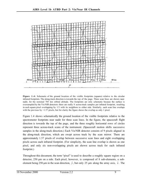
Figure 1.4: Schematic of the ground location of the visible footprints (squares) relative to the circular<br />
infrared footprints. The along-track direction is towards the top of the page. Three scan lines are shown nearnadir,<br />
for the nominal 705 km orbital altitude. The footprints are only schematic because the surface is<br />
oversampled by the Vis/NIR detectors: there are really 8 across-track samples per infrared footprint, resulting<br />
in each square pixel overlapping by 1/3 with its neighbors to either side. Similarly, each scan line overlaps<br />
with the previous by ~1.57 pixels, but for clarity the figure shows the overlap as only 1 pixel.<br />
Figure 1.4 shows schematically the ground location of the visible footprints relative to the<br />
spectrometer footprints near nadir for three scan lines. In the figure, the spacecraft flight<br />
direction is towards the top of the page, and the three roughly horizontal rows of circles<br />
represent three across-track scans of the instrument. (Spacecraft motion shifts successive<br />
samples in the along-track direction.) Each Vis/NIR detector consists of 9 pixels aligned in<br />
the along-track direction, which are swept across track by the scan mirror. There are<br />
approximately 1.57 pixels of overlap between successive scan lines and eight overlapping<br />
pixels across each infrared footprint. (For simplicity, the scan line overlap is shown as one<br />
pixel, and only six non-overlapping pixels are shown across track for each infrared<br />
footprint.)<br />
Throughout this document, the term “pixel” is used to describe a roughly square region on a<br />
detector, 250 µm on a side. Each pixel, however, is composed of 8 sub-elements, a subelement<br />
being 250 µm in the scan direction, ŷ, but only 25 µm along the array axis, ˆx. The<br />
10 November 2000 Version 2.2 9