Download Burst QPSK Modulator Data Sheet
Download Burst QPSK Modulator Data Sheet
Download Burst QPSK Modulator Data Sheet

Create successful ePaper yourself
Turn your PDF publications into a flip-book with our unique Google optimized e-Paper software.
SEMICONDUCTOR<br />
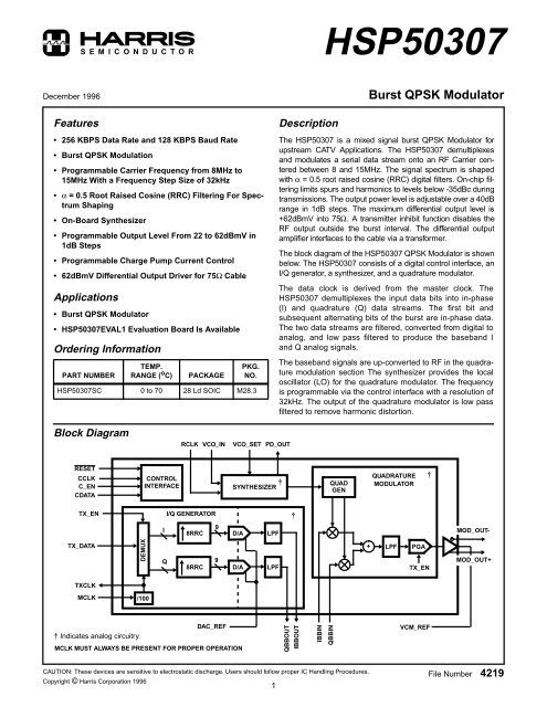
HSP50307<br />
December 1996<br />
<strong>Burst</strong> <strong>QPSK</strong> <strong>Modulator</strong><br />
Features<br />
• 256 KBPS <strong>Data</strong> Rate and 128 KBPS Baud Rate<br />
• <strong>Burst</strong> <strong>QPSK</strong> Modulation<br />
• Programmable Carrier Frequency from 8MHz to<br />
15MHz With a Frequency Step Size of 32kHz<br />
• α = 0.5 Root Raised Cosine (RRC) Filtering For Spectrum<br />
Shaping<br />
• On-Board Synthesizer<br />
• Programmable Output Level From 22 to 62dBmV in<br />
1dB Steps<br />
• Programmable Charge Pump Current Control<br />
• 62dBmV Differential Output Driver for 75Ω Cable<br />
Applications<br />
• <strong>Burst</strong> <strong>QPSK</strong> <strong>Modulator</strong><br />
• HSP50307EVAL1 Evaluation Board Is Available<br />
Ordering Information<br />
PART NUMBER<br />
TEMP.<br />
RANGE ( o C)<br />
PACKAGE<br />
PKG.<br />
NO.<br />
HSP50307SC 0 to 70 28 Ld SOIC M28.3<br />
Description<br />
The HSP50307 is a mixed signal burst <strong>QPSK</strong> <strong>Modulator</strong> for<br />
upstream CATV Applications. The HSP50307 demultiplexes<br />
and modulates a serial data stream onto an RF Carrier centered<br />
between 8 and 15MHz. The signal spectrum is shaped<br />
with α = 0.5 root raised cosine (RRC) digital filters. On-chip filtering<br />
limits spurs and harmonics to levels below -35dBc during<br />
transmissions. The output power level is adjustable over a 40dB<br />
range in 1dB steps. The maximum differential output level is<br />
+62dBmV into 75Ω. A transmitter inhibit function disables the<br />
RF output outside the burst interval. The differential output<br />
amplifier interfaces to the cable via a transformer.<br />
The block diagram of the HSP50307 <strong>QPSK</strong> <strong>Modulator</strong> is shown<br />
below. The HSP50307 consists of a digital control interface, an<br />
I/Q generator, a synthesizer, and a quadrature modulator.<br />
The data clock is derived from the master clock. The<br />
HSP50307 demultiplexes the input data bits into in-phase<br />
(I) and quadrature (Q) data streams. The first bit and<br />
subsequent alternating bits of the burst are in-phase data.<br />
The two data streams are filtered, converted from digital to<br />
analog, and low pass filtered to produce the baseband I<br />
and Q analog signals.<br />
The baseband signals are up-converted to RF in the quadrature<br />
modulation section The synthesizer provides the local<br />
oscillator (LO) for the quadrature modulator. The frequency<br />
is programmable via the control interface with a resolution of<br />
32kHz. The output of the quadrature modulator is low pass<br />
filtered to remove harmonic distortion.<br />
Block Diagram<br />
RCLK<br />
VCO_IN<br />
VCO_SET PD_OUT<br />
RESET<br />
CCLK<br />
C_EN<br />
CDATA<br />
CONTROL<br />
INTERFACE<br />
†<br />
SYNTHESIZER<br />
QUAD<br />
GEN<br />
QUADRATURE<br />
MODULATOR<br />
†<br />
TX_EN<br />
I/Q GENERATOR<br />
†<br />
I<br />
8RRC<br />
9<br />
D/A<br />
LPF<br />
MOD_OUT-<br />
TX_DATA<br />
DEMUX<br />
Q<br />
8RRC<br />
9<br />
D/A<br />
LPF<br />
+<br />
LPF<br />
PGA<br />
TX_EN<br />
MOD_OUT+<br />
TXCLK<br />
MCLK<br />
/100<br />
† Indicates analog circuitry.<br />
DAC_REF<br />
MCLK MUST ALWAYS BE PRESENT FOR PROPER OPERATION<br />
QBBOUT<br />
IBBOUT<br />
IBBIN<br />
QBBIN<br />
VCM_REF<br />
CAUTION: These devices are sensitive to electrostatic discharge. Users should follow proper IC Handling Procedures.<br />
Copyright © Harris Corporation 1996<br />
1<br />
File Number 4219
HSP50307<br />
Pinout<br />
28 LEAD SOIC<br />
TOP VIEW<br />
MCLK<br />
1<br />
28<br />
CCLK<br />
TXCLK<br />
2<br />
27<br />
CDATA<br />
TX_EN<br />
3<br />
26<br />
C_EN<br />
TX_DATA<br />
4<br />
25<br />
DVCC<br />
RESET<br />
5<br />
24<br />
RCLK<br />
DGND<br />
6<br />
23<br />
AGND<br />
AVCC<br />
7<br />
22<br />
PD_OUT<br />
AGND<br />
8<br />
21<br />
VCO_IN<br />
IBBOUT<br />
9<br />
20<br />
VCO_SET<br />
QBBOUT<br />
10<br />
19<br />
AVCC<br />
QBBIN<br />
11<br />
18<br />
MOD_OUT-<br />
IBBIN<br />
12<br />
17<br />
MOD_OUT+<br />
DAC_REF<br />
13<br />
16<br />
AVDD<br />
VCM_REF<br />
14<br />
15<br />
AGND<br />
Pin Description<br />
SYMBOL TYPE DESCRIPTION<br />
MCLK I Master clock input (25.6MHz). (D)<br />
TXCLK O PSK data clock (256kHz) for PSK_DATA_IN. (D)<br />
TX_EN I Transmit enable. When high, the modulator output is enabled. This pin should be high for the entire burst. The signal is<br />
extended internally until data has fully exited the part before turning off for spurious free turn on and turn off. (D)<br />
TX_DATA I 256 KBPS serial data input. (D)<br />
RESET I Digital reset pin (active low). The part is reset immediately on assertion of the reset pin. The output of the part is<br />
disabled on the assertion of reset. The part will come out of reset 2 master clock periods after the reset is deasserted.<br />
Reprogramming (see Control Interface section) is needed after deassertion of reset for proper operation.<br />
(D)<br />
DGND I Negative supply for the digital filters and control. (P)<br />
AVCC I Positive supply for the quadrature modulator. AVCC should be tied to +5V analog. (P)<br />
AGND I Negative supply for the quadrature modulator. AGND is tied to GND. (P)<br />
IBBOUT O I baseband filtered output (A).<br />
QBBOUT O Q baseband filtered output. (A)<br />
QBBIN I Q baseband modulator input. (A)<br />
IBBIN I I baseband modulator input. (A)<br />
DAC_REF O D/A reference node. A 0.1µF capacitor to ground is suggested. (A)<br />
VCM_REF O <strong>Modulator</strong> common mode reference node. A 0.1µF capacitor to ground is suggested. (A)<br />
AGND I Negative supply for the cable interface. (P)<br />
AVDD I Positive supply for the cable interface (+9V analog). (P)<br />
MOD_OUT+ O Positive output drive pin for the cable interface. (A)<br />
MOD_OUT- O Negative output drive pin for the cable interface. (A)<br />
2
HSP50307<br />
Pin Description (Continued)<br />
SYMBOL TYPE DESCRIPTION<br />
AVCC I Positive supply for the synthesizer (+5V analog). (P)<br />
VCO_SET I/O VCO free running frequency set resistor (normally 6.25kΩ). (D)<br />
VCO_IN I Voltage-controlled oscillator control voltage. (D)<br />
PD_OUT O Phase/frequency detector output. (D)<br />
AGND I Negative supply for the synthesizer. (P)<br />
RCLK I Synthesizer reference clock input (2.048MHz). (D)<br />
DVCC I Positive supply for the digital filters and control (+5V digital). (P)<br />
C_EN I Control interface enable for 3 wire interface. See Control Interface section. (D)<br />
CDATA I Serial data input for 3 wire interface. See Control Interface section. (D)<br />
CCLK I 3 wire interface clock. See Control Interface section. (D)<br />
NOTE: (A) = analog, (D) = digital, (P) = power.<br />
Functional Description<br />
The HSP50307 is designed to transmit 256 KBPS data<br />
using <strong>QPSK</strong> modulation on a programmable carrier over<br />
75Ω cable lines. The incoming 256 KBPS data is first<br />
demultiplexed into in-phase (I) and quadrature (Q) data<br />
streams. The burst <strong>QPSK</strong> modulator shapes the two<br />
128 KBPS demultiplexed data streams using interpolateby-8<br />
root-raised cosine (RRC) filters with α = 0.5. The<br />
resulting 1.024MHz data streams are sent through D/A<br />
converters and are then sent through low-pass<br />
reconstruction filters for over 40dB image rejection. The<br />
baseband analog output and input pins allow the signals to<br />
be AC coupled. The returning analog signal is upconverted<br />
by an analog quadrature modulator. The control section is<br />
configured by loading 23 bits of information via a three-wire<br />
interface. These bits configure the DSP filter section, the<br />
carrier frequency, the analog synthesizer, and the output<br />
driver sections.<br />
COEFFICIENT VALUE<br />
0.8<br />
0.7<br />
0.6<br />
0.5<br />
0.4<br />
0.3<br />
0.2<br />
0.1<br />
0<br />
-0.1<br />
-0.2<br />
1 8 16 24 32 40 48 56 64<br />
TAP NUMBER<br />
FIGURE 1. NORMALIZED IMPULSE RESPONSE OF THE RRC<br />
INTERPOLATION FILTER WITH α = 0.5<br />
Digital Filters<br />
REF -15.0 dBm<br />
# AT 60dB<br />
MKR 8.0960MHz<br />
-16.83dBm<br />
The burst <strong>QPSK</strong> modulator uses an interpolate-by-8 digital<br />
RRC filter on both the I and Q data streams. The shaping<br />
factor is set to α = 0.5. The FIR order of the digital RRC filter<br />
is 64. Figure 1 shows the impulse response of the RRC filter.<br />
PEAK<br />
LOG<br />
5dB/<br />
Figure 2 is a spectrum analyzer plot of the modulator output<br />
for a baud rate of 128 kbaud and a pseudorandom data pattern.<br />
The 128kHz 3dB bandwidth and 192kHz stopband<br />
edges are readily apparent.<br />
WA SB<br />
SC FS<br />
CORR<br />
CENTER 8.0960MHz<br />
#RES BW 300Hz<br />
VBW 300Hz<br />
SPAN 400.0kHz<br />
SWP 13.3s<br />
FIGURE 2. SPECTRUM OF 8.096MHz RANDOM DATA MODU-<br />
LATED CARRIER<br />
3
HSP50307<br />
Control Interface<br />
The <strong>QPSK</strong> modulator is configured via a serial three wire<br />
interface. When C_EN is high, 23 bits are shifted in at the<br />
CDATA pin on the falling edge of CCLK. Figure 3 shows the<br />
timing diagram for loading the serial configuration data.<br />
Table 1 describes the 23-bit serial configuration data. See<br />
the Synthesizer Section for more details on the frequency<br />
control bits.<br />
TABLE 1. 23 BIT SERIAL DATA CONTROL INTERFACE<br />
DESCRIPTION<br />
BIT<br />
POSITION FUNCTION DESCRIPTION<br />
D0-D2<br />
(Note)<br />
D3-D9<br />
D10<br />
D11<br />
D12<br />
D13-D18<br />
Synthesizer<br />
Control Bits<br />
Synthesizer<br />
Control Bits<br />
Synthesizer<br />
Enable<br />
Charge Pump<br />
Current<br />
Control<br />
Three-State<br />
Control<br />
Attenuation<br />
Control<br />
Pre-scaler control register.<br />
A = (0 to 5), D2 is the MSB.<br />
Feedback counter control register.<br />
M = (41 to 103) D9 is the MSB.<br />
Active high. This bit activates chip bias<br />
networks for normal operation. D10 = 0<br />
places part in low power mode.<br />
D11 = 0 sets charge pump current to<br />
500µA.<br />
D11 = 1 sets charge pump current to<br />
1mA.<br />
D12 = 0 three-states the charge pump<br />
output when a pump up and down<br />
command occur simultaneously.<br />
D12 = 1 disables three-state.<br />
Controls output power level. The binary<br />
value of the register corresponds to<br />
an attenuation amount. For example,<br />
000100 corresponds to 4dB attenuation<br />
from the maximum 62dBmV level.<br />
D18 is the MSB.<br />
D19-D21 Reserved Used for test/diagnostic purposes.<br />
Set to 000.<br />
D22<br />
DSP Shut<br />
Down<br />
Test mode; D22 = 0 sets the burst<br />
<strong>QPSK</strong> modulator in normal mode.<br />
D22 = 1 disables the digital filter.<br />
Synthesizer<br />
The synthesizer generates the quadrature LO’s for<br />
modulating the baseband data to RF. The carrier frequency<br />
is phase locked to the reference clock (RCLK). The carrier<br />
frequency, F C , has a frequency range of 8MHz to 15MHz<br />
with a resolution of 32kHz. Equation 1 gives the relationship<br />
between F C and the frequency of RCLK and the frequency<br />
control bits, M and A.<br />
F C = 6M -------------------------------- ( + 1)<br />
+ A F<br />
64 REF , (EQ. 1)<br />
where F REF equals the frequency of RCLK. Also, M and A<br />
can be determined by<br />
M +<br />
A --- 6<br />
=<br />
64<br />
-----<br />
6<br />
F C<br />
-------------- – 1.<br />
F REF<br />
“A” ranges from 0 to 5 and “M” ranges from 41 to 103. A and<br />
M are programmed via control bits D0-D2 and D3-D9,<br />
respectively. Values outside these ranges are invalid.<br />
I/Q Generator<br />
The I/Q Generator Section demultiplexes and time aligns the<br />
256 KBPS input data into two data streams, I and Q. The<br />
first data bit following the assertion of the TX_EN signal is<br />
the I data of the first I/Q pair. Each I/Q pair determines the<br />
phase angle of the <strong>QPSK</strong> transmission signal. The relationship<br />
between I/Q pairs and phase angles is shown in<br />
Table 2. Since the <strong>QPSK</strong> encoding requires a pair of I and Q<br />
information to transmit one symbol, an even number of data<br />
bits must be provided for each burst.<br />
TABLE 2. <strong>QPSK</strong> ENCODING<br />
I Q PHASE<br />
0 0 45 o<br />
0 1 135 o<br />
1 0 -45 o<br />
1 1 -135 o<br />
(EQ. 2)<br />
NOTE: D0 is the first bit shifted into the part.<br />
T CCH<br />
CCLK<br />
T CDS<br />
T CDH<br />
C_DATA<br />
D22 D21<br />
D20<br />
D19<br />
D3<br />
D2 D1 D0<br />
C_EN<br />
FIGURE 3. CONTROL INTERFACE TIMING DIAGRAM<br />
4
HSP50307<br />
Applications Example<br />
+5V DIGITAL<br />
25.6MHz<br />
OSC<br />
0.1µF<br />
DGND<br />
1<br />
2<br />
MCLK<br />
TXCLK<br />
CCLK<br />
CDATA<br />
28<br />
27<br />
CONTROL<br />
PROC.<br />
DATA<br />
SOURCE<br />
3<br />
TX_EN<br />
C_EN<br />
26<br />
4<br />
TX_DATA<br />
DVCC<br />
25<br />
+5V ANALOG<br />
5<br />
RESET<br />
RCLK<br />
24<br />
2.048MHz<br />
OSC<br />
DGND<br />
0.1µF<br />
6<br />
7<br />
8<br />
9<br />
DGND<br />
AVCC<br />
AGND<br />
IBBOUT<br />
AGND<br />
PD_OUT<br />
VCO_IN<br />
VCO_SET<br />
23<br />
22<br />
21<br />
20<br />
2kΩ<br />
100pF<br />
6.25kΩ<br />
0.01µF<br />
+5V ANALOG<br />
0.01µF<br />
0.1µF<br />
0.1µF<br />
0.1µF<br />
0.1µF<br />
10<br />
11<br />
12<br />
13<br />
14<br />
QBBOUT<br />
QBBIN<br />
IBBIN<br />
DAC_REF<br />
VCM_REF<br />
AVCC<br />
MOD_OUT-<br />
MOD_OUT+<br />
AVDD<br />
AGND<br />
19<br />
18<br />
17<br />
16<br />
15<br />
37.5Ω 0.1µF<br />
37.5Ω 0.1µF<br />
0.1µF<br />
CABLE<br />
TRANSFORMER<br />
+9V ANALOG<br />
RFOUT<br />
AGND<br />
AGND<br />
FIGURE 4. APPLICATIONS EXAMPLE OF THE HSP50307<br />
Figure 4 shows an applications example of the HSP50307.<br />
The MCLK source operates at 25.6MHz, and the RCLK<br />
operates at 2.048MHz. 0.1µF capacitors are connected from<br />
the IBBOUT to IBBIN and the QBBOUT to QBBIN, providing<br />
AC coupling to the analog upconverter section of the<br />
HSP50307.<br />
The control processor sends the 23-bit control word via the<br />
three-wire interface. The data source receives the 256kHz<br />
TXCLK from the HSP50307 and transmits data and enable<br />
signal at the 256kHz rate.<br />
The DAC_REF and VCM_REF are connected to 0.1µF<br />
capacitors to ground. Each of the differential drivers are<br />
loaded with a 37.5Ω resistor and a 0.1µF capacitor. The<br />
37.5Ω resistors provide matching to the 75Ω cable. The<br />
capacitors perform AC coupling. The drive paths are sent to<br />
the cable transformer for data transmissions.<br />
Table 3 shows the general functional specifications for the<br />
applications example shown in Figure 4. It gives an overview<br />
of what is being accomplished but does not specify an exact<br />
carrier frequency or other programmable functions. These<br />
specifications are met given a valid control word combination<br />
and the applications circuit shown in Figure 4. Table 4 summarizes<br />
the performance of the applications example shown<br />
in Figure 4. Again, these specifications are met given a valid<br />
programmed mode.<br />
NOTE: The HSP50307 is sensitive to layout. Users must<br />
make sure the input signals do not couple back into the<br />
output signals. The performance of the HSP50307 is<br />
also sensitive to the decoupling capacitors between<br />
1) QBBOUT and QBBIN and 2) IBBOUT and IBBIN. The<br />
values shown in Figure 4 are recommended.<br />
5
HSP50307<br />
TABLE 3. GENERAL FUNCTIONAL SPECIFICATIONS<br />
AVCC, DVCC = +5V, AVDD = +9V; RCLK = 2.048MHz; MCLK = 25.6MHz; T A = 0 o C To 70 o C<br />
PARAMETER MIN TYP MAX UNIT<br />
<strong>QPSK</strong> Carrier Frequency 8.0 - 15 (Note) MHz<br />
<strong>QPSK</strong> Carrier Frequency Step Size - 32 - kHz<br />
Modulation Bandwidth - 192 - kHz<br />
Raised Cosine FIlter Response Excess Bandwidth (α) - 0.5 - -<br />
Transmit Level Adjust - 40 - dB<br />
<strong>Data</strong> Rate - 256 - KBPS<br />
Baud Rate - 128 - KBPS<br />
NOTE: May operate up to 20MHz.<br />
TABLE 4. <strong>QPSK</strong> PERFORMANCE SPECIFICATIONS<br />
AVCC, DVCC = +5V, AVDD = +9V; RCLK = 2.048MHz; MCLK = 25.6MHz; T A = 0 o C to 70 o C<br />
PARAMETER MIN TYP MAX UNITS<br />
Output Spurious Signals Less Than 54MHz - -40 -35 dBc<br />
Output Spurious Signals Greater Than 54MHz - -60 -50 dBc<br />
Off Mode Spurs - - -30 dBmV<br />
Transmit Level (D18-D13 = 000000) 59 62 65 dBmV<br />
Output Gain Adjust Relative Accuracy -0.5 0.2 0.5 dB<br />
Absolute Output Accuracy at Any Step -3.0 ±2 3.0 dB<br />
<strong>QPSK</strong> Carrier Phase Noise at 10kHz Offset - - -75 dBc/Hz<br />
<strong>QPSK</strong> Carrier Phase Noise at 1kHz Offset - - -60 dBc/Hz<br />
<strong>QPSK</strong> <strong>Modulator</strong> Carrier Suppression 35 40 - dBc<br />
<strong>QPSK</strong> I/Q Amplitude Imbalance - - 0.5 dB<br />
<strong>QPSK</strong> I/Q Phase Imbalance - - 2.0 Degree<br />
<strong>QPSK</strong> Passband Amplitude Ripple -0.3 - 0.3 dB<br />
6
HSP50307<br />
Absolute Maximum Ratings<br />
5V Supply Voltage . . . . . . . . . . . . . . . . . . . . . . . . . . . . . . . . . . . 6.0V<br />
9V Supply Voltage . . . . . . . . . . . . . . . . . . . . . . . . . . . . . . . . . . 11.0V<br />
ESD Classification . . . . . . . . . . . . . . . . . . . . . . . . . . . Class 1, HBM<br />
Operating Conditions<br />
Temperature Range . . . . . . . . . . . . . . . . . . . . . . . . . . . .0 o C to 70 o C<br />
Thermal Information<br />
Thermal Resistance (Typical, Note 1)<br />
θ JA ( o C/W)<br />
SOIC Package . . . . . . . . . . . . . . . . . . . . . . . . . . . . . 70<br />
Maximum Junction Temperature . . . . . . . . . . . . . . . . . . . . . . . 150 o C<br />
Maximum Storage Temperature Range . . . . . . . . . .-65 o C to 150 o C<br />
Maximum Lead Temperature (Soldering 10s) . . . . . . . . . . . . . 300 o C<br />
(SOIC - Lead Tips Only)<br />
CAUTION: Stresses above those listed in “Absolute Maximum Ratings” may cause permanent damage to the device. This is a stress only rating and operation<br />
of the device at these or any other conditions above those indicated in the operational sections of this specification is not implied.<br />
NOTE:<br />
1. θ JA is measured with the component mounted on an evaluation PC board in free air.<br />
DC Electrical Specifications<br />
RCLK = 2.048MHz; MCLK = 25.6MHz; T A = 0 o C to 70 o C<br />
PARAMETER SYMBOL/PIN MIN TYP MAX UNIT<br />
5V Supply Voltage AVCC, DVCC 4.75 5.0 5.25 V<br />
9V Supply Voltage AVDD 8.55 9.0 9.45 V<br />
5V Supply Current I AVCC , I DVCC - 55 - mA DC<br />
9V Supply Current I AVDD - 60 - mA DC<br />
Logical One Input Voltage V IH 3.325 - - V<br />
Logical Zero Input Voltage V IL - - 1.575 V<br />
Output High Voltage V OH 2.6 - - V<br />
Output Low Voltage V OL - - 0.4 V<br />
AC Electrical Specifications<br />
AVCC, DVCC = +5V, AVDD = +9V; RCLK = 2.048MHz; MCLK = 25.6MHz;<br />
T A = 0 o C to 70 o C<br />
PARAMETER SYMBOL MIN TYP MAX UNIT<br />
RESET Pulse Width t RES 500 - - ns<br />
MCLK Period (25.6MHz) t MCP - 39.1 - ns<br />
RCLK Period (2.048MHz) t RCP - 488 - ns<br />
RCLK High t RCH 98 - - ns<br />
RCLK Low t RCL 98 - - ns<br />
CCLK Period (5MHz) t CCP 200 - - ns<br />
CCLK High t CCH 150 - - ns<br />
CCLK Low t CCL 150 - - ns<br />
CDATA Setup to CCLK t CDS 50 - - ns<br />
CDATA Hold from CCLK t CDH - - 50 ns<br />
C_EN Strobe Edge to CCLK t CES -100 - 100 ns<br />
TXCLK Period (256kHz) t DCP - 3910 - ns<br />
TXCLK High t DCH 195 - - ns<br />
7
HSP50307<br />
AC Electrical Specifications<br />
AVCC, DVCC = +5V, AVDD = +9V; RCLK = 2.048MHz; MCLK = 25.6MHz;<br />
T A = 0 o C to 70 o C (Continued)<br />
PARAMETER SYMBOL MIN TYP MAX UNIT<br />
TXCLK Low t DCL 195 - - ns<br />
TX_DATA Setup to TXCLK t DIS 150 - - ns<br />
TX_DATA Hold from TXCLK t DIH 0 - - ns<br />
Waveforms<br />
t MCP<br />
1 2<br />
MCLK<br />
t RCP<br />
PART IS ACTIVE AGAIN<br />
t RCH<br />
t RCL<br />
t RES<br />
RESET<br />
RCLK<br />
FIGURE 5. RESET AND MCLK WAVEFORMS<br />
FIGURE 6. RCLK WAVEFORM<br />
t CCP<br />
t CCL<br />
t CCH<br />
CCLK<br />
t CDS<br />
t CDH<br />
t DCP<br />
CDATA<br />
TXCLK<br />
t DCL<br />
t DCH<br />
t DIS<br />
t DIH<br />
C_EN<br />
TX_DATA<br />
t CES<br />
FIGURE 7. CONFIGURATION WAVEFORMS<br />
FIGURE 8. TRANSMIT DATA WAVEFORMS<br />
8
Small Outline Plastic Packages (SOIC)<br />
HSP50307<br />
N<br />
INDEX<br />
AREA<br />
1 2 3<br />
e<br />
D<br />
B<br />
0.25(0.010) M C A<br />
M<br />
E<br />
-B-<br />
-A-<br />
-C-<br />
SEATING PLANE<br />
A<br />
B S<br />
H 0.25(0.010) M B<br />
A1<br />
0.10(0.004)<br />
NOTES:<br />
1. Symbols are defined in the “MO Series Symbol List” in Section<br />
2.2 of Publication Number 95.<br />
2. Dimensioning and tolerancing per ANSI Y14.5M-1982.<br />
3. Dimension “D” does not include mold flash, protrusions or gate<br />
burrs. Mold flash, protrusion and gate burrs shall not exceed<br />
0.15mm (0.006 inch) per side.<br />
4. Dimension “E” does not include interlead flash or protrusions. Interlead<br />
flash and protrusions shall not exceed 0.25mm (0.010<br />
inch) per side.<br />
5. The chamfer on the body is optional. If it is not present, a visual<br />
index feature must be located within the crosshatched area.<br />
6. “L” is the length of terminal for soldering to a substrate.<br />
7. “N” is the number of terminal positions.<br />
8. Terminal numbers are shown for reference only.<br />
9. The lead width “B”, as measured 0.36mm (0.014 inch) or greater<br />
above the seating plane, shall not exceed a maximum value of<br />
0.61mm (0.024 inch)<br />
10. Controlling dimension: MILLIMETER. Converted inch dimensions<br />
are not necessarily exact.<br />
α<br />
L<br />
M<br />
h x 45 o<br />
C<br />
M28.3 (JEDEC MS-013-AE ISSUE C)<br />
28 LEAD WIDE BODY SMALL OUTLINE PLASTIC PACKAGE<br />
INCHES<br />
MILLIMETERS<br />
SYMBOL MIN MAX MIN MAX NOTES<br />
A 0.0926 0.1043 2.35 2.65 -<br />
A1 0.0040 0.0118 0.10 0.30 -<br />
B 0.013 0.0200 0.33 0.51 9<br />
C 0.0091 0.0125 0.23 0.32 -<br />
D 0.6969 0.7125 17.70 18.10 3<br />
E 0.2914 0.2992 7.40 7.60 4<br />
e 0.05 BSC 1.27 BSC -<br />
H 0.394 0.419 10.00 10.65 -<br />
h 0.01 0.029 0.25 0.75 5<br />
L 0.016 0.050 0.40 1.27 6<br />
N 28 28 7<br />
α 0 o 8 o 0 o 8 o -<br />
Rev. 0 12/93<br />
All Harris Semiconductor products are manufactured, assembled and tested under ISO9000 quality systems certification.<br />
Harris Semiconductor products are sold by description only. Harris Semiconductor reserves the right to make changes in circuit design and/or specifications at<br />
any time without notice. Accordingly, the reader is cautioned to verify that data sheets are current before placing orders. Information furnished by Harris is<br />
believed to be accurate and reliable. However, no responsibility is assumed by Harris or its subsidiaries for its use; nor for any infringements of patents or other<br />
rights of third parties which may result from its use. No license is granted by implication or otherwise under any patent or patent rights of Harris or its subsidiaries.<br />
Sales Office Headquarters<br />
NORTH AMERICA<br />
Harris Semiconductor<br />
P. O. Box 883, Mail Stop 53-210<br />
Melbourne, FL 32902<br />
TEL: 1-800-442-7747<br />
(407) 729-4984<br />
FAX: (407) 729-5321<br />
For general information regarding Harris Semiconductor and its products, call 1-800-4-HARRIS<br />
EUROPE<br />
Harris Semiconductor<br />
Mercure Center<br />
100, Rue de la Fusee<br />
1130 Brussels, Belgium<br />
TEL: (32) 2.724.2111<br />
FAX: (32) 2.724.22.05<br />
ASIA<br />
Harris Semiconductor PTE Ltd.<br />
No. 1 Tannery Road<br />
Cencon 1, #09-01<br />
Singapore 1334<br />
TEL: (65) 748-4200<br />
FAX: (65) 748-0400<br />
SEMICONDUCTOR<br />
9