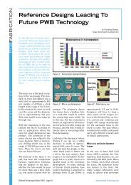
Uniformity Of Ni Plating Thickness in High Aspect Ratio PTH
Uniformity Of Ni Plating Thickness in High Aspect Ratio PTH
Uniformity Of Ni Plating Thickness in High Aspect Ratio PTH

You also want an ePaper? Increase the reach of your titles
YUMPU automatically turns print PDFs into web optimized ePapers that Google loves.
PCBFABRICATION<br />
<strong>Uniformity</strong> <strong>Of</strong> <strong>Ni</strong> <strong>Plat<strong>in</strong>g</strong> <strong>Thickness</strong><br />
<strong>in</strong> <strong>High</strong> <strong>Aspect</strong> <strong>Ratio</strong> <strong>PTH</strong><br />
by David M. Lee, Frank L. Coll<strong>in</strong>s, Ann E. Dietrich, John T. Folkerts, Walter A. Johnston, Richard J Saunders,<br />
Johns Hopk<strong>in</strong>s Applied Physics Laboratory<br />
<strong>Ni</strong>ckel plat<strong>in</strong>g is often used on<br />
PWBs to <strong>in</strong>crease wear resistance<br />
and to prevent diffusion between<br />
copper and other plated metals.<br />
The nickel plat<strong>in</strong>g is often present<br />
<strong>in</strong> through holes as well as on the<br />
surface, such as when the entire<br />
PWB panel is nickel/gold plated or<br />
when press fit p<strong>in</strong>s are used for assembly.<br />
When the plated through<br />
holes are evaluated by microsection<strong>in</strong>g,<br />
it often becomes apparent<br />
that the nickel plat<strong>in</strong>g is not uniform.<br />
It tends to be much th<strong>in</strong>ner<br />
<strong>in</strong> the middle of the hole than on<br />
the surface of the board, and may<br />
not meet m<strong>in</strong>imum thickness requirements.<br />
We take a look at the<br />
effect of various plat<strong>in</strong>g parameters<br />
and chemical additives on through<br />
hole plat<strong>in</strong>g uniformity.<br />
As advanced pr<strong>in</strong>ted wir<strong>in</strong>g board<br />
(PWB) designs become more complex,<br />
the thickness of the board<br />
has <strong>in</strong>creased due to the greater<br />
number of layers. The plated<br />
through hole (<strong>PTH</strong>) diameters have<br />
become much smaller to accommodate<br />
the greater density of advanced<br />
designs. As the <strong>PTH</strong> aspect ratio<br />
(board thickness divided by hole diameter)<br />
<strong>in</strong>creases, it becomes more<br />
difficult to obta<strong>in</strong> a uniform plat<strong>in</strong>g<br />
<strong>in</strong> the hole.<br />
The performance specifications of<br />
MIL-PRF-55110G for high reliability<br />
<strong>PTH</strong> nickel deposits requires<br />
a m<strong>in</strong>imum plat<strong>in</strong>g thickness of<br />
5 microns <strong>in</strong> the hole. This m<strong>in</strong>imum<br />
thickness is difficult to obta<strong>in</strong><br />
when plat<strong>in</strong>g high aspect ratio holes<br />
without result<strong>in</strong>g <strong>in</strong> excessive plat<strong>in</strong>g<br />
on the board surface. The difference<br />
<strong>in</strong> the plat<strong>in</strong>g thickness <strong>in</strong><br />
the hole and the board surface is<br />
referred to as the surface-to-hole<br />
thickness ratio (SHTR). The SHTR<br />
is determ<strong>in</strong>ed by divid<strong>in</strong>g the deposit<br />
thickness on the surface by<br />
the deposit thickness <strong>in</strong> the hole.<br />
The goal when fabricat<strong>in</strong>g high reliability<br />
<strong>PTH</strong>s is to keep this ratio as<br />
low as possible.<br />
PWB designs that require selective<br />
<strong>PTH</strong>s are particularly challeng<strong>in</strong>g<br />
to obta<strong>in</strong> a low SHTR because of the<br />
Figure 1 – Direct agitation<br />
(left)<br />
Figure 2 – Indirect agitation<br />
(below)<br />
high current density on the surface<br />
of the board around the hole. As a<br />
result of the <strong>in</strong>creased current density<br />
on the holes annular r<strong>in</strong>g, the<br />
plat<strong>in</strong>g is much thicker on the surface<br />
then <strong>in</strong> the centre of the hole.<br />
Figure 3 – Test coupon<br />
Figure 4 – Pre plate process flow<br />
If the plat<strong>in</strong>g on the surface layer<br />
becomes too thick while try<strong>in</strong>g to<br />
obta<strong>in</strong> the m<strong>in</strong>imum thickness <strong>in</strong><br />
the centre of the hole a number<br />
of problems can arise such as: a<br />
decrease <strong>in</strong> the hole diameter so<br />
components won’t fit, <strong>in</strong>creased<br />
stress between the plated layers,<br />
and mushroom plat<strong>in</strong>g on surface<br />
pads that can trap photo resist.<br />
<strong>Plat<strong>in</strong>g</strong> formulas with high throw<strong>in</strong>g<br />
power are designed to overcome the<br />
limitations of conventional plat<strong>in</strong>g<br />
formulas. <strong>High</strong> throw plat<strong>in</strong>g baths<br />
distribute the current more evenly,<br />
result<strong>in</strong>g <strong>in</strong> a uniform plat<strong>in</strong>g layer<br />
<strong>in</strong> the hole. Some high throw plat<strong>in</strong>g<br />
baths reduce the amount of organic<br />
additives (carriers, brighteners,<br />
levellers) <strong>in</strong> their chemistry to<br />
obta<strong>in</strong> the higher throw<strong>in</strong>g power.<br />
OnBoard Technology July 2008 - page 18<br />
www.Onboard-Technology.com
Tables 1 and 2 – Experiment matrix – surface to hole thickness ratio: 28 mil hole<br />
PCBFABRICATION<br />
Therefore when utilis<strong>in</strong>g these<br />
types of plat<strong>in</strong>g baths, a complete<br />
analysis of the deposit must be performed<br />
to ensure that it meets all<br />
the performance and specification<br />
requirements.<br />
A number of plat<strong>in</strong>g experiments<br />
were conducted with the goal of<br />
achiev<strong>in</strong>g the lowest possible SHTR<br />
while meet<strong>in</strong>g the plat<strong>in</strong>g specifications<br />
required for flight qualified<br />
PWBs. Also, tests were conducted<br />
to determ<strong>in</strong>e the highest aspect<br />
ratio through hole that can be reliably<br />
plated.<br />
shock and thermal stress tests were<br />
performed.<br />
<strong>Plat<strong>in</strong>g</strong> equipment<br />
All experiments were conducted <strong>in</strong><br />
a 5 gallon tank. Agitation was supplied<br />
by a recirculation filter pump<br />
with a centre tank sparger. The<br />
sparger can be adjusted for direct<br />
agitation (Figure 1) or <strong>in</strong>direct agitation<br />
(Figure 2) to the substrate.<br />
The nickel anodes were sulfur-free<br />
and anode bags were used. Kraft<br />
Dynatronix models DUP10-1-3 and<br />
DP20-5-10 power supplies were<br />
used.<br />
Two plat<strong>in</strong>g formulas were compared<br />
<strong>in</strong> these experiments. A sulfamate<br />
bath was selected because of<br />
the low stress deposits it produces<br />
and a bromide bath specifically designed<br />
for high throw plat<strong>in</strong>g. Each<br />
bath was also compared with the<br />
addition of a gra<strong>in</strong> ref<strong>in</strong>er additive.<br />
The plat<strong>in</strong>g parameters that were<br />
varied for these experiments were:<br />
rectification, direct current (DC)<br />
vs pulse current, solution agitation<br />
and current density.<br />
Figure 5 – Bromide bath SHTR with a 28 mil hole <strong>in</strong> a 62 mil board<br />
Figure 6 – Bromide bath SHTR with a 28 mil hole <strong>in</strong> a 93 mil board<br />
Analysis of the nickel deposit <strong>in</strong>cluded<br />
stress measurements of the<br />
as plated nickel and after a thermal<br />
cycle, surface roughness, thermal<br />
www.Onboard-Technology.com<br />
OnBoard Technology July 2008 - page 19
PCBFABRICATION<br />
Figure 7 – 28 mil hole <strong>in</strong> a 62 mil board plated <strong>in</strong> the sulfamate bath with<br />
DC at 5 ASF us<strong>in</strong>g <strong>in</strong>direct agitation (left, 20 x magnification)<br />
Figure 8 – 28 mil hole <strong>in</strong> a 62 mil board plated <strong>in</strong> the bromide bath with DC<br />
at 5 ASF us<strong>in</strong>g <strong>in</strong>direct agitation (right, 20 x magnification)<br />
Figure 9 – 6 micron thick nickel deposit <strong>in</strong> the center of a 28 mil hole <strong>in</strong> a<br />
62 mil board (left, 20 x magnification)<br />
Figure 10 – 10 mil hole <strong>in</strong> a 93 mil board pulse plated <strong>in</strong> the bromide bath<br />
at 15 ASF with direct agitation (right, 5 x magnification)<br />
Experiment details<br />
This study used polyimide boards of<br />
two thicknesses 62 mils and 93mils.<br />
The board design variables <strong>in</strong>cluded<br />
seven hole sizes of 8, 10, 15, 20, 28,<br />
40 and 50 mils represent<strong>in</strong>g aspect<br />
ratios from 1.25:1 up to 11.37:1. The<br />
boards were drilled, electroless copper<br />
plated, patterned, electrolytically<br />
copper plated as a 12”x18” panel. The<br />
panels were then routed to 2”x 4”<br />
test coupons. The test coupons were<br />
patterned with dry film photoresist<br />
for selective plat<strong>in</strong>g (Figure 3).<br />
<strong>Plat<strong>in</strong>g</strong> experiments were conducted<br />
with sulfamate and a bromide<br />
plat<strong>in</strong>g formulas. Current<br />
densities of 5, 15, and 30 amps per<br />
square foot (ASF) were compared.<br />
Pulse plat<strong>in</strong>g with a 10% duty cycle<br />
(0.1 sec. on-0.9 sec. off) was<br />
compared to direct current. The<br />
solution flow was varied utilis<strong>in</strong>g<br />
direct and <strong>in</strong>direct agitation as<br />
shown <strong>in</strong> Figures 1 and 2. Tests<br />
were conducted with the addition<br />
of a gra<strong>in</strong> ref<strong>in</strong>er <strong>in</strong> each bath as<br />
well.<br />
Pre-plate preparation consisted<br />
of a standard acid cleaner, microetch<br />
and an acid activation with a<br />
2 m<strong>in</strong>. deionised water r<strong>in</strong>se between<br />
each step (Figure 4).<br />
Figure 11 – 10 mil hole <strong>in</strong> a 93 mil board pulse plated <strong>in</strong> the bromide bath<br />
at 15 ASF with direct agitation (left, 10 x magnification)<br />
Figure 12 – 10 mil hole <strong>in</strong> a 93 mil board pulse plated <strong>in</strong> the bromide bath<br />
at 15 ASF with direct agitation (20 x magnification)<br />
The plat<strong>in</strong>g thickness on the surface<br />
of the coupon was measured<br />
with a Fischerscope XDLM x-ray<br />
fluorescence system. The test coupons<br />
were then microsectioned<br />
and optical microscopy was used to<br />
determ<strong>in</strong>e the nickel deposit thickness<br />
<strong>in</strong> the through hole. The 28<br />
mil hole was used as the control.<br />
Test results<br />
The experimental matrix listed <strong>in</strong><br />
Table1 shows the SHTR measured<br />
from a 28 mil hole <strong>in</strong> the test coupon.<br />
The results <strong>in</strong> Table 1 clearly<br />
show that the SHTR is much lower<br />
with the bromide bath compared<br />
to the sulfamate bath. The best results<br />
were obta<strong>in</strong>ed <strong>in</strong> the bromide<br />
bath with DC plat<strong>in</strong>g and a current<br />
density of 5 ASF with <strong>in</strong>direct agitation.<br />
Pulse plat<strong>in</strong>g at 15 ASF with<br />
direct agitation also resulted <strong>in</strong> a<br />
low SHTR.<br />
Indirect agitation appears to <strong>in</strong>crease<br />
the throw<strong>in</strong>g power when<br />
DC plat<strong>in</strong>g at a low current density.<br />
Conversely, direct agitation improved<br />
the throw<strong>in</strong>g power when<br />
pulse plat<strong>in</strong>g. This could be attributed<br />
to the fact that when pulse<br />
plat<strong>in</strong>g, the metal ions are replaced<br />
at the cathode film dur<strong>in</strong>g the off<br />
cycle. Therefore the <strong>in</strong>creased solution<br />
flow would <strong>in</strong>crease the plat<strong>in</strong>g<br />
efficiency. When DC plat<strong>in</strong>g,<br />
too much solution flow actually<br />
reduces the throw<strong>in</strong>g power.<br />
Table 2 shows the experimental<br />
matrix with the gra<strong>in</strong> ref<strong>in</strong>er additive.<br />
The addition of the gra<strong>in</strong> ref<strong>in</strong>er<br />
did not improve the SHTR <strong>in</strong><br />
either of the plat<strong>in</strong>g baths. Further<br />
studies will be performed with different<br />
additives.<br />
Figures 5 and 6 show the bromide<br />
bath SHTR with a 28 mil hole <strong>in</strong> a<br />
62 mil and a 93 mil board.<br />
Figures 7 and 8 compare a 28 mil<br />
hole <strong>in</strong> a 62 mil board plated under<br />
the same conditions (DC at 5<br />
ASF us<strong>in</strong>g <strong>in</strong>direct agitation) <strong>in</strong> the<br />
sulfamate bath and <strong>in</strong> the bromide<br />
bath. It can be seen that the nickel<br />
deposit from the bromide bath<br />
OnBoard Technology July 2008 - page 20<br />
www.Onboard-Technology.com
Table 3 – Plated thru hole SHTR<br />
Table 4 – <strong>Ni</strong>ckel deposit stress<br />
measurements<br />
5 ASF with <strong>in</strong>direct agitation. Figures<br />
10, 11 and 12 show a 10 mil<br />
hole <strong>in</strong> a 93 mil board, pulse plated<br />
<strong>in</strong> the bromide bath at 15 ASF with<br />
direct agitation.<br />
All of the holes <strong>in</strong> the test coupons<br />
from the DC plat<strong>in</strong>g at 5 ASF with<br />
<strong>in</strong>direct agitation and pulse plat<strong>in</strong>g<br />
at 15 ASF with direct agitation<br />
were evaluated to determ<strong>in</strong>e<br />
the greatest aspect ratio that these<br />
processes were capable of plat<strong>in</strong>g.<br />
Table 3 shows that both plat<strong>in</strong>g<br />
conditions were capable of deposit<strong>in</strong>g<br />
a uniform nickel layer <strong>in</strong><br />
holes with an aspect ratio as great<br />
as 9.1:1. Reliable plat<strong>in</strong>g results<br />
could not be obta<strong>in</strong>ed from the 8<br />
mil holes with an aspect ratio of<br />
11.37:1.<br />
Figure 13 – DC plated <strong>in</strong> the<br />
bromide bath at 5ASF with <strong>in</strong>direct<br />
agitation<br />
Figure 14 – Pulse plated <strong>in</strong> the<br />
bromide bath at 15 ASF with direct<br />
agitation<br />
PCBFABRICATION<br />
Although, the SHTR <strong>in</strong>creased as<br />
the aspect ratio became greater,<br />
the values are still well with<strong>in</strong> acceptable<br />
limits.<br />
is much more uniform than the<br />
sulfamate bath. The SHTR of the<br />
sample <strong>in</strong> Figure 7 is over 4.3 compared<br />
to the SHTR of 1.25 <strong>in</strong> Figure<br />
8. Figure 9 shows a 6 micron<br />
thick nickel deposit <strong>in</strong> the centre<br />
of a 28 mil hole <strong>in</strong> a 62 mil board<br />
plated with the same conditions as<br />
the sample <strong>in</strong> Figure 8.<br />
As noted <strong>in</strong> the experimental matrix<br />
listed <strong>in</strong> Table 1, pulse plat<strong>in</strong>g<br />
<strong>in</strong> the bromide bath at 15 ASF<br />
with direct agitation also resulted<br />
<strong>in</strong> a low SHTR. The uniformity of<br />
the nickel deposit <strong>in</strong> the high aspect<br />
ratio <strong>PTH</strong> plated with these<br />
conditions was comparable to the<br />
DC plat<strong>in</strong>g at a current density of<br />
Table 5 – Surface roughness<br />
measurements<br />
Deposit analysis<br />
Sample coupons were prepared<br />
from 3 <strong>in</strong>ch silicon wafers that<br />
were metallised with 3 microns<br />
of copper. The wafers were plated<br />
<strong>in</strong> the bromide bath with DC and<br />
pulse current at 5 and 15 ASF. The<br />
stress <strong>in</strong> the nickel deposit was<br />
measured with a KLA Tencor FLX<br />
Film Stress Measurement System.<br />
The stress was first measured as<br />
plated. The samples were then annealed<br />
at 125°C for 150 hours and<br />
remeasured.<br />
Although results <strong>in</strong> Table 4 show<br />
an <strong>in</strong>crease <strong>in</strong> the tensile stress after<br />
the anneal, the stress values are<br />
well with<strong>in</strong> the acceptable range<br />
for each of the plat<strong>in</strong>g conditions.<br />
The nickel deposit should exhibit<br />
good thermal shock properties.<br />
Scann<strong>in</strong>g Electron Microscopy<br />
(SEM) was used to determ<strong>in</strong>e the<br />
deposit morphology. Figure 13<br />
shows a SEM of a sample plated <strong>in</strong><br />
the bromide bath us<strong>in</strong>g DC at 5ASF<br />
with <strong>in</strong>direct agitation. The deposit<br />
has a gra<strong>in</strong> size of about 1 micron.<br />
The rough surface can be attributed<br />
to the lack of additives (brighteners<br />
and levellers) <strong>in</strong> the bath.<br />
Figure 14 shows a sample that was<br />
pulse plated <strong>in</strong> the bromide bath<br />
at 15 ASF with direct agitation.<br />
The gra<strong>in</strong> size is about 0.5 micron<br />
at the higher current density with<br />
pulse plat<strong>in</strong>g.<br />
The surface roughness was measured<br />
with a DEKTAT 6M Stylus<br />
Profilometer. A 1000 micron scan<br />
was taken <strong>in</strong> 5 areas of each wafer.<br />
The results <strong>in</strong> Table 5 show that<br />
the surface roughness was greater<br />
at the lower current density irrespective<br />
of the rectification used.<br />
Reliability<br />
Sample coupons were subjected to<br />
thermal shock and thermal stress<br />
tests. The thermal shock test consisted<br />
of a temperature cycle of<br />
+125°C to -65°C for 100 cycles with<br />
www.Onboard-Technology.com<br />
OnBoard Technology July 2008 - page 21
PCBFABRICATION<br />
Figure 16 – 62 mil board with a press fit connector p<strong>in</strong> after the thermal<br />
shock test<br />
Figure 17 – 93 mil board with a press fit connector p<strong>in</strong> after the thermal<br />
shock test<br />
Figure 15 – 28 mil hole <strong>in</strong> a 62 mil<br />
board after thermal shock and<br />
thermal stress test<br />
a 15 m<strong>in</strong> dwell time. The thermal<br />
stress test conducted per IPC-TM-<br />
650 consisted of a 6 hour bake at<br />
120°C, then a solder float at 290°C<br />
for 10 seconds.<br />
Evaluation of the coupon microsections<br />
showed no signs of crack<strong>in</strong>g<br />
or delam<strong>in</strong>ation. Figure 15 shows a<br />
28 mil hole <strong>in</strong> a 62 mil board plated<br />
us<strong>in</strong>g DC at 5 ASF with <strong>in</strong>direct<br />
agitation after thermal shock and<br />
thermal stress tests.<br />
Sample boards of 62mils and 91mils<br />
were fabricated and selective nickel<br />
and gold plated for a press fit connector.<br />
The boards consisted of<br />
one hundred 28 mil holes for an<br />
Airborne press fit connector. The<br />
nickel plat<strong>in</strong>g was from the bromide<br />
bath us<strong>in</strong>g DC at 5 ASF with<br />
<strong>in</strong>direct agitation. The nickel plat<strong>in</strong>g<br />
thickness was 6 microns. Hard<br />
gold was plated over the nickel.<br />
The press fit connector was <strong>in</strong>serted<br />
<strong>in</strong>to the boards. Each board was<br />
subjected to the thermal shock test.<br />
Evaluation of the microsections<br />
showed no signs of crack<strong>in</strong>g or<br />
delam<strong>in</strong>ation. Figure 16 shows the<br />
62 mil board and Figure 17 shows<br />
the 93 mil board after the thermal<br />
shock test.<br />
This article is based on a paper orig<strong>in</strong>ally<br />
presented at the IPC Pr<strong>in</strong>ted Circuits Expo,<br />
APEX and the Designer’s Summit 2008<br />
Plac<strong>in</strong>g LEDs On Flex Circuits<br />
The future, from a light<strong>in</strong>g prospective,<br />
will look drastically different<br />
thanks to LED technology, which<br />
is be<strong>in</strong>g used <strong>in</strong> more and more<br />
applications all over the world. In<br />
the last few years, Essemtec has<br />
delivered production equipment<br />
to the LED <strong>in</strong>dustry for various applications.<br />
Most of this production<br />
equipment was custom design. For<br />
example, a customer produc<strong>in</strong>g sensor strips began<br />
with screen pr<strong>in</strong>t<strong>in</strong>g of the solder paste on a high end<br />
SP200 pr<strong>in</strong>ter then dispens<strong>in</strong>g with a jet dispenser, pick<br />
& place of the LED and UV cur<strong>in</strong>g of the adhesive on a<br />
FLX 2010 based module. Next step was laser solder<strong>in</strong>g<br />
of the pads on a 3rd party laser solder<strong>in</strong>g system. The<br />
sensor strips were based on a foil substrate consist<strong>in</strong>g<br />
of up to 56 strips with 3 LEDs each and the target cycle<br />
time was 5.4 seconds per sensor strip. Essemtec delivered<br />
a system with a cycle time of 4.1 seconds per strip,<br />
achiev<strong>in</strong>g 34% higher production capacity.<br />
The concept of the solution was based on the FLX<br />
2010, equipped with a movable<br />
vacuum table, UV chamber and<br />
dispens<strong>in</strong>g unit with jet valve. The<br />
foil is placed on a carrier. This<br />
carrier can be used for the previous<br />
and the follow<strong>in</strong>g processes.<br />
The vacuum table and the carrier<br />
are pressurised permanently. The<br />
movement of the table is software<br />
controlled. The GUI was customized<br />
for this application. The head unit is equipped<br />
with a jet valve and the pick & place Z axis. The vacuum<br />
pump was located outside of the mach<strong>in</strong>e and runs<br />
constantly. The customisation was based on feasibility<br />
and cost considerations. The system is flexible and can<br />
be upgraded easily.<br />
Essemtec<br />
Mosenstrasse 20, CH-6287 Aesch/LU – Schweiz<br />
Tel. +41 41 919 60 60, Fax +41 41 919 60 50<br />
<strong>in</strong>fo@essemtec.com<br />
www.essemtec.com<br />
OnBoard Technology July 2008 - page 22<br />
www.Onboard-Technology.com