Microvia Filling - OnBoard Technology
Microvia Filling - OnBoard Technology
Microvia Filling - OnBoard Technology
- TAGS
- microvia
- onboard
- www.yumpu.com

You also want an ePaper? Increase the reach of your titles
YUMPU automatically turns print PDFs into web optimized ePapers that Google loves.
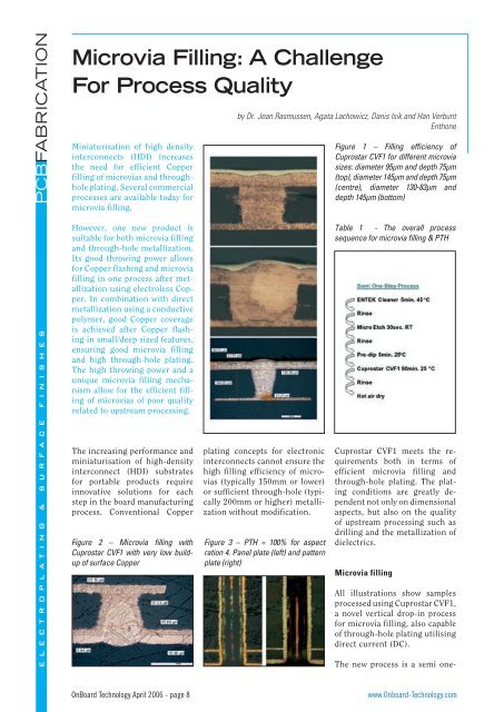
PCBFABRICATIONE L E C T R O P L A T I N G & S U R F A C E F I N I S H E SFigure 6 - Void caused by poor seeding (left) and a good fill from good seeding(right). Dimensions Ø 145mm and depth 85mmper build-up at the upper corners ofthe microvia (Figure 7) and a voidwill occur during filling, as shownin Figure 6.Direct metallizationAn alternative to E’Cu metallizationis surface treatment with aconductive polymer such as EnvisionHDI. A thin conductive polymerof a few 100 Angstroms thicknessis selectively deposited on thedielectric and not on the exposedCopper, which eliminates the riskof Copper-Copper interface separationcaused by surface contamination.The high conductivity of the polymerallows for direct electrolyticCopper plating, which reduces theoverall processing time and numberof necessary processing steps.Selective formation of a conductivepolymer is proven by AugerAnalysis (Figure 8). The conductiveFigure 9 (below) - Cuprostar CVF1 as aflash process after E’Cu metallizationpolymer contains Sulphur and theanalysis shows continuous conductivecoating on both resin and glassfibres but not on the Cu surface.The selectivity of the conductivepolymer on resin and glass fibresand not on Copper inner layers inmultilayer boards reduces Copper-Copper interface separation duringthermal expansion.The very good throwing powerof the CVF1 process allows it tobe used for microvia filling andthrough-hole metallization as wellas flash processes after E’Cu (Figure9).Efficiency and versatilityThe microvia filling and throughholeplating efficiency of CuprostarCVF1 has been highlighted forfeatures with varying dimensions:small, large, and deep microviasFigure 7 – Poor coverage after Cuflashin an electrolyte with lowthrowing powerand through-holes.Also documented is its ability tofill microvias after poor qualityprocessing downstream in the overallprocess. <strong>Microvia</strong>s with roughcell walls, caused by exposed glassfibres, large overhang and innerlayer penetration resulting from inappropriateconditions during laserdrilling, can be filled efficiently.Its throwing power allows it to beused as a flash process and a fillingprocess in combination with E’Cuconceptsfor the metallization ofdielectrics.In direct metallization processesusing Envision HDI, the goodthrowing power of CVF1 resultsin a uniform Copper seeding/flash(also in deep and small sized features)and efficient microvia fillingand through-hole plating, withoutthe use of E’Cu.Figure 8 (above) - Auger surface analysis for conductive polymer containingSulphur<strong>OnBoard</strong> <strong>Technology</strong> April 2006 - page 10www.Onboard-<strong>Technology</strong>.com