Technology And Infrastructure For Embedded Passive Components
Technology And Infrastructure For Embedded Passive Components
Technology And Infrastructure For Embedded Passive Components

You also want an ePaper? Increase the reach of your titles
YUMPU automatically turns print PDFs into web optimized ePapers that Google loves.
PCBFABRICATION<br />
I N T E G R A T I O N O F P A S S I V E A N D A C T I V E D E V I C E S<br />
<strong>Technology</strong> <strong>And</strong> <strong>Infrastructure</strong> <strong>For</strong><br />
<strong>Embedded</strong> <strong>Passive</strong> <strong>Components</strong><br />
A range of integrated and embedded<br />
passive component technology<br />
options are available and<br />
a number of technological and<br />
commercial barriers exist that<br />
are gating the development and<br />
uptake of this exciting new technology.<br />
In the following, we take<br />
a look at these technology options<br />
and barriers and make recommendations<br />
for building the<br />
embedded passives infrastructure.<br />
Discrete Surface Mount passive<br />
components make up over 90<br />
per cent of the total component<br />
count on a typical PCB today.<br />
These components also account<br />
for some 30 per cent of all solder<br />
joints and occupy close to 40 per<br />
cent of the total board area. These<br />
discrete passive components can<br />
prove even more significant in<br />
cell phone boards where up to 95<br />
percent of the total component<br />
count, 80 per cent of the board<br />
area and 70 per cent of the board<br />
assembly costs may be attributed<br />
to the passive components.<br />
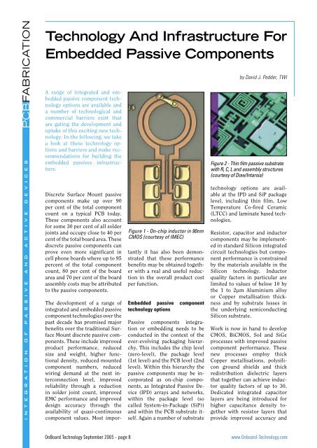
Figure 1 - On-chip inductor in 90nm<br />
CMOS (courtesy of IMEC)<br />
The development of a range of<br />
integrated and embedded passive<br />
component technologies over the<br />
past decade has promised major<br />
benefits over the traditional Surface<br />
Mount discrete passive components.<br />
These include improved<br />
product performance, reduced<br />
size and weight, higher functional<br />
density, reduced mounted<br />
component numbers, reduced<br />
wiring demand at the next interconnection<br />
level, improved<br />
reliability through a reduction<br />
in solder joint count, improved<br />
EMC performance and improved<br />
design accuracy through the<br />
availability of quasi-continuous<br />
component values. Most importantly<br />
it has also been demonstrated<br />
that these performance<br />
benefits may be obtained together<br />
with a real and useful reduction<br />
in the overall product cost<br />
per function.<br />
<strong>Embedded</strong> passive component<br />
technology options<br />
<strong>Passive</strong> components integration<br />
or embedding needs to be<br />
conducted in the context of the<br />
ever-evolving packaging hierarchy.<br />
This includes the chip level<br />
(zero-level), the package level<br />
(1st level) and the PCB level (2nd<br />
level). Within this hierarchy the<br />
passive components may be incorporated<br />
as on-chip components,<br />
as Integrated <strong>Passive</strong> Device<br />
(IPD) arrays and networks,<br />
within the package level (so<br />
called System-in-Package (SiP))<br />
and within the PCB substrate itself.<br />
Again a number of substrate<br />
by David J. Pedder, TWI<br />
Figure 2 - Thin film passive substrate<br />
with R, C, L and assembly structures<br />
(courtesy of Dow/Intarsia)<br />
technology options are available<br />
at the IPD and SiP package<br />
level, including thin film, Low<br />
Temperature Co-fired Ceramic<br />
(LTCC) and laminate based technologies.<br />
Resistor, capacitor and inductor<br />
components may be implemented<br />
in standard Silicon integrated<br />
circuit technologies but component<br />
performance is constrained<br />
by the materials available in the<br />
Silicon technology. Inductor<br />
quality factors in particular are<br />
limited to values of below 10 by<br />
the 1 to 2µm Aluminium alloy<br />
or Copper metallisation thickness<br />
and by substrate losses in<br />
the underlying semiconducting<br />
Silicon substrate.<br />
Work is now in hand to develop<br />
CMOS, BiCMOS, SoI and SiGe<br />
processes with improved passive<br />
component performance. These<br />
new processes employ thick<br />
Copper metallisations, polysilicon<br />
ground shields and thick<br />
redistribution dielectric layers<br />
that together can achieve inductor<br />
quality factors of up to 30.<br />
Dedicated integrated capacitor<br />
layers are being introduced for<br />
higher capacitance density together<br />
with resistor layers that<br />
provide improved accuracy and<br />
OnBoard <strong>Technology</strong> September 2005 - page 8<br />
www.Onboard-<strong>Technology</strong>.com
lower temperature coefficient of<br />
resistance.<br />
<strong>Passive</strong> inductor and capacitor<br />
components are less amenable<br />
to scaling than active IC components<br />
and so the use of such onchip<br />
passive components adds a<br />
chip area (and associated cost)<br />
overhead of up to 0.5mm 2 per<br />
component. On-chip passives<br />
are therefore best employed in<br />
circuits where a few, performance<br />
critical components are<br />
required, for example in Voltage<br />
Controlled Oscillators (VCOs)<br />
(Figure 1).<br />
The closely related integrated<br />
passive thin film technology category<br />
employs Silicon-like processing<br />
technology to provide<br />
precision passive component<br />
arrays, networks, IPDs and substrates<br />
for high functional density<br />
SiP applications. High resistivity<br />
Silicon wafers, glass wafers<br />
or large area panel substrates are<br />
employed for the thin film manufacturing<br />
process. A sequence<br />
of metal and dielectric layers are<br />
deposited by a combination of<br />
sputter deposition, electroplating,<br />
anodisation, chemical vapour<br />
deposition and spin coating<br />
and patterned by photolithography<br />
and wet and dry etching<br />
techniques in typically 5 to 8<br />
masking operations. Conductor<br />
and interlayer dielectric layers<br />
are in the 2 to 10µm thickness<br />
range.<br />
The Thin Film approach<br />
The thin film resistor materials<br />
include nichrome and tantalum<br />
nitride for low TCR resistor<br />
components at 25 to 100 ohms/<br />
square. The capacitor and interlayer<br />
dielectric layers include anodised<br />
aluminium oxide or tantalum<br />
pentoxide, silicon nitride<br />
and benzocyclobutene (BCB) or<br />
polyimide materials to realise<br />
capacitor components with capacitance<br />
densities between 4pF<br />
and 1,000pF/mm 2 . The conductor<br />
materials that provide the<br />
passive component electrodes,<br />
Figure 3 - Assembled LTCC Bluetooth<br />
module<br />
the ground plane, inductor elements,<br />
controlled impedance<br />
interconnection traces and active<br />
component and next level<br />
interconnection pads include<br />
Aluminium and Copper with the<br />
addition of Nickel-Gold surface<br />
finish layers where required for<br />
wire bondability and solderability.<br />
The thin film technology option<br />
provides a full range of precision<br />
passive components (Figure 2)<br />
with inductor quality factors of<br />
up to 70 through the use of low<br />
loss substrate materials. This<br />
technology option is well suited<br />
for high-density passives applications<br />
(over 100 passives/cm 2 )<br />
in the realisation of small matching<br />
and filtering networks (a few<br />
mm 2 ) and for networks, arrays<br />
and SiP substrates up to 1cm 2<br />
in area. The technology has the<br />
advantage of compatibility with<br />
active device technology and<br />
the emerging MEMS technologies<br />
and is manufactured today<br />
by a number of IC companies to<br />
leverage and add value to their<br />
Silicon IC product offerings.<br />
The Low Temperature Co-fired<br />
Ceramic approach<br />
The LTCC integrated passives<br />
technology options has its origins<br />
in thick film hybrid technology<br />
using screen printed and<br />
fired thick film materials. The<br />
LTCC material itself comprises<br />
an unfired (so called “green”)<br />
glass-ceramic material held together<br />
with a polymeric binder.<br />
Interlayer vias are drilled or<br />
punched and metallised and<br />
thick film conductor, resistor<br />
and dielectric patterns are printed<br />
onto the green LTCC layers.<br />
Multiple LTCC layers are then<br />
laminated and fired to produce a<br />
fully dense multilayer substrate<br />
structure with integrated passive<br />
components and interconnection<br />
structures. Additional surface<br />
layer components may then be<br />
printed and fired and accessible<br />
components laser trimmed as<br />
required. Lithographic patterning<br />
and zero-in-plane-shrinkage<br />
technologies have been introduced<br />
in recent years to increase<br />
pattern accuracy to below 25µm<br />
feature size and to improve dimensional<br />
control.<br />
A wide range of thick film resistor,<br />
dielectric and conductor<br />
materials is available. Resistor<br />
materials cover the range from<br />
10 ohms/square to 1 Mohm/<br />
square, although buried resistor<br />
layers are best limited to a narrower<br />
range. Paraelectric and<br />
ferroelectric dielectric materials<br />
are available with dielectric<br />
constants from 5 to in excess of<br />
2,000 at a typical minimum layer<br />
thickness of 10µm. Silver and<br />
silver alloy conductor layers are<br />
widely employed in LTCC technology<br />
with a typical layer thickness<br />
of 10 to 15µm. This substantial<br />
metal thickness leads to<br />
high inductor quality factors at<br />
~ 1GHz frequencies.<br />
The LTCC technology offers a<br />
cost effective, rigid, stable and repeatable<br />
substrate medium that<br />
includes a wide range of passive<br />
component elements, with the<br />
option of component trimming<br />
for circuit tuning. The LTCC<br />
medium also provides a built-in<br />
active and discrete passive device<br />
packaging and interconnec-<br />
Figure 4 - PCB embedded resistor<br />
component<br />
PCBFABRICATION<br />
I N T E G R A T I O N O F P A S S I V E A N D A C T I V E D E V I C E S<br />
www.Onboard-<strong>Technology</strong>.com<br />
OnBoard <strong>Technology</strong> September 2005 - page 9
PCBFABRICATION<br />
tion structure. This technology<br />
option has been adopted for the<br />
volume manufacture of a range<br />
of RF SiP modules for applications<br />
such as the Bluetooth RF<br />
front-end and related transceiver<br />
functions with substrate areas of<br />
up to 2cm 2 (Figure 3).<br />
I N T E G R A T I O N O F P A S S I V E A N D A C T I V E D E V I C E S<br />
The Laminate <strong>Embedded</strong> <strong>Passive</strong>s<br />
approach<br />
The last category of integrated<br />
passive component technologies<br />
is the printed circuit board or<br />
laminate embedded passives category.<br />
Here the additional materials<br />
required are built into the<br />
original laminate layers that are<br />
subsequently bonded together<br />
and processed to form the multilayer<br />
circuit board structure.<br />
This is done in such a way that<br />
relatively minor modifications<br />
to established PCB processes<br />
are required. This technology<br />
is employed for the realisation<br />
of board level passive integration<br />
and in the manufacture of<br />
larger area SiP substrates (up<br />
to 25cm 2 ). <strong>Embedded</strong> passive<br />
component densities of up to 5<br />
passives per cm 2 are typical in<br />
today’s technology.<br />
PCB embedded resistor components<br />
are realised using ~100nm<br />
electroless Nickel-Phosphorus<br />
deposits, sputter deposited nichrome<br />
or chemical combustion<br />
deposited platinum alloy layers.<br />
Resistivity levels of 50 to 1,000<br />
ohms/square are achieved. Polymer<br />
thick film resistor materials<br />
at over 10µm thickness and covering<br />
a much wider range of resistivity<br />
values are also available.<br />
<strong>Embedded</strong> capacitor technology<br />
options include distributed planar<br />
capacitor technologies to provide<br />
board level decoupling and<br />
Figure 5 - Inductor model (left) and measured and modelled performance (right)<br />
discrete capacitor technologies.<br />
The former category is the most<br />
advanced and employs unfilled<br />
and ferroelectric filled polymer<br />
dielectric layers at above 10µm<br />
thickness. Thin film paraelectric<br />
and ferroelectric technologies<br />
have also been developed. Inductor<br />
components can use the PCB<br />
metallisation structures already<br />
available within the board technology,<br />
although due attention<br />
must be given to component<br />
design and to ground plane and<br />
routing keep-outs. A very interesting<br />
PCB embedded passives<br />
technology class has also been<br />
developed based around the cofiring<br />
of thick film materials<br />
onto Copper foil prior to laminate<br />
manufacture.<br />
The PCB embedded technology<br />
offers a large area manufacturing,<br />
low cost per unit area technology<br />
option that is well suited<br />
to board level and SiP passive<br />
component integration. A range<br />
of materials and technology options<br />
are available from a number<br />
of PCB materials vendors.<br />
<strong>Embedded</strong> resistor technologies<br />
and distributed capacitor technologies<br />
are finding first applications<br />
for board level termination<br />
and pull-up resistor functions<br />
and for board level decoupling<br />
(Figure 4). Discrete capacitor<br />
and inductor applications are<br />
presently less well developed.<br />
<strong>Technology</strong> barriers and<br />
infrastructure requirements<br />
Discrete Surface Mount passive<br />
components are provided in a<br />
limited number of standardised<br />
component form factors (0603,<br />
0402, 0201 etc) and this makes<br />
it possible to quickly change<br />
passive component values and<br />
realise simple design iterations<br />
during New Product Introduction<br />
(NPI) without requiring<br />
changes in the board design and<br />
layout. The adoption of any of<br />
various classes of integrated or<br />
embedded passive component<br />
technology on the other hand<br />
precludes changing component<br />
values without making mask<br />
changes and completing further<br />
substrate or panel processing<br />
runs since the components, by<br />
definition, are contained within<br />
the substrate structure. This can<br />
result in increased design iteration<br />
cycle time and drives the<br />
need for a “right-first-time” design<br />
approach for integrated passives<br />
technologies, together with<br />
an NPI strategy than minimises<br />
the need for design iterations.<br />
A “right-first-time” design approach<br />
can be achieved through<br />
the development of a technology<br />
specific “design-kit” that<br />
includes the full range of passive<br />
and interconnection and<br />
assembly component symbols<br />
OnBoard <strong>Technology</strong> September 2005 - page 10<br />
www.Onboard-<strong>Technology</strong>.com
that will be used during circuit<br />
schematic capture and simulation.<br />
Each component symbol<br />
contains the appropriate equivalent<br />
circuit electrical model, and<br />
may be linked into component<br />
physical layout generation. The<br />
generation of such a design-kit<br />
requires a well-defined process<br />
architecture with a stable manufacturing<br />
process that has known<br />
or at least tightly specified process<br />
capabilities. <strong>Technology</strong><br />
characterisation substrates or<br />
panels have to be produced that<br />
include the full range of passive<br />
component families and interconnection<br />
and assembly components<br />
that span the full range<br />
of component geometries within<br />
each family. Electrical measurements<br />
are followed by equivalent<br />
circuit model generation and the<br />
construction of the design-kit.<br />
This design approach has been<br />
ably demonstrated in the thin<br />
film technology option outlined<br />
earlier in this paper. Of particular<br />
note has been the generation of<br />
scalable, parameterised, lumped<br />
element equivalent circuit models<br />
in which the primary component<br />
value and all the component<br />
parasitics are expressed as<br />
a function of a single parameter,<br />
for example the capacitor dimension<br />
or the number of turns in<br />
the inductor. This in turn allows<br />
straightforward design optimisation.<br />
An example lumped element<br />
equivalent circuit model<br />
for a thin film inductor and the<br />
close agreement of the measured<br />
and modelled s-parameters are<br />
illustrated in Figure 5.<br />
A typical design flow then includes<br />
design specification,<br />
schematic capture, simulation<br />
and optimisation, component<br />
generation and layout, re-simulation<br />
as required followed by<br />
design-for-test, design tolerance<br />
analysis and yield modelling<br />
(Figure 6). The inclusion<br />
of individual circuit functional<br />
blocks and design variants in the<br />
NPI substrate or panel layout<br />
also minimises the need for design<br />
iterations. An example of a<br />
Figure 7 - Thin film passives filter layout, measured and modelled<br />
performance<br />
thin film integrated passives filter<br />
design that shows very close<br />
agreement between the circuit<br />
simulation and measured results<br />
from the first substrate processing<br />
run is illustrated in Figure 7.<br />
A more complex SiP module example<br />
containing a range of integrated<br />
passive circuit elements<br />
for matching, filtering, biasing<br />
and interconnection functions<br />
and a number of Silicon and gallium<br />
arsenide active devices is illustrated<br />
in Figure 8.<br />
The integrated passives industry<br />
will need to put in place a set<br />
of design-kits for each specific<br />
technology definition and architecture<br />
variant in a similar way<br />
that each Silicon integrated circuit<br />
process today has it’s own<br />
process specific models and design<br />
kits. The demonstration of<br />
compatible and common formfit-and-function<br />
will also be required<br />
from multiple suppliers<br />
so that end-users have more<br />
Figure 6 - Integrated passives<br />
design flow<br />
than one single source of technology<br />
supply. This requirement<br />
has already been demonstrated<br />
and met for both thin film and<br />
for LTCC technology implementations<br />
from different sources.<br />
Conclusions<br />
A wide range of integrated and<br />
embedded passive component<br />
technology options are available<br />
that promise a range of<br />
performance and costs benefits<br />
across the packaging hierarchy.<br />
The development of technology<br />
specific design-kits provides a<br />
route to right-first-time design<br />
and removes one key barrier to<br />
the successful commercial exploitation<br />
of this exciting new<br />
technology. The establishment<br />
of design and supply chain partnerships<br />
will play an important<br />
part in the establishment of the<br />
integrated and embedded passives<br />
infrastructure.<br />
Figure 8 - Thin Film SiP HIPERLAN<br />
module (courtesy Dow/Intarsia)<br />
PCBFABRICATION<br />
I N T E G R A T I O N O F P A S S I V E A N D A C T I V E D E V I C E S<br />
www.Onboard-<strong>Technology</strong>.com<br />
OnBoard <strong>Technology</strong> September 2005 - page 11