Reference Designs Leading To Future PWB Technology - OnBoard ...
Reference Designs Leading To Future PWB Technology - OnBoard ...
Reference Designs Leading To Future PWB Technology - OnBoard ...

You also want an ePaper? Increase the reach of your titles
YUMPU automatically turns print PDFs into web optimized ePapers that Google loves.
PCBFABRICATION<br />
<strong>Reference</strong> <strong>Designs</strong> <strong>Leading</strong> <strong>To</strong><br />
<strong>Future</strong> <strong>PWB</strong> <strong>Technology</strong><br />
At the Wireless Terminal Business<br />
Unit of Texas Instruments in<br />
Denmark, new packaging technology<br />
combined with new chip<br />
functions are tested in reference<br />
designs. This takes place one<br />
to three years before the products<br />
enter the market in larger<br />
quantities. During early product<br />
development only a small number<br />
of <strong>PWB</strong>s has to be made to<br />
demonstrate the functionality of<br />
the hardware and to provide software<br />
engineers with a “reference<br />
design” PCB that will enable engineers<br />
to develop the software<br />
for new mobile phone applications.<br />
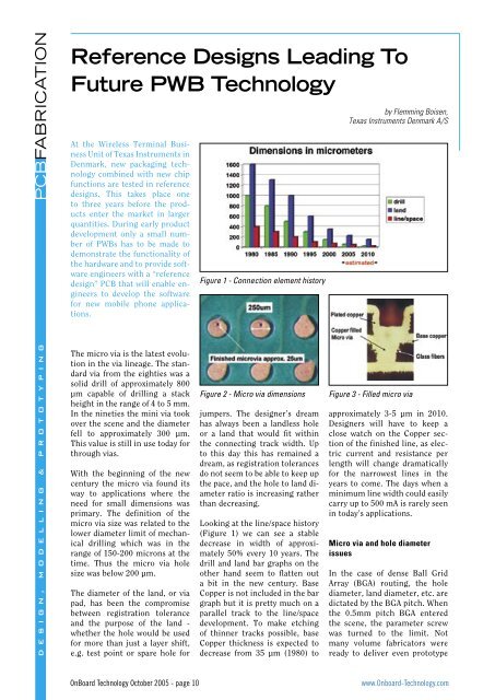
Figure 1 - Connection element history<br />
by Flemming Boisen,<br />
Texas Instruments Denmark A/S<br />
D E S I G N , M O D E L L I N G & P R O T O T Y P I N G<br />
The micro via is the latest evolution<br />
in the via lineage. The standard<br />
via from the eighties was a<br />
solid drill of approximately 800<br />
µm capable of drilling a stack<br />
height in the range of 4 to 5 mm.<br />
In the nineties the mini via took<br />
over the scene and the diameter<br />
fell to approximately 300 µm.<br />
This value is still in use today for<br />
through vias.<br />
With the beginning of the new<br />
century the micro via found its<br />
way to applications where the<br />
need for small dimensions was<br />
primary. The definition of the<br />
micro via size was related to the<br />
lower diameter limit of mechanical<br />
drilling which was in the<br />
range of 150-200 microns at the<br />
time. Thus the micro via hole<br />
size was below 200 µm.<br />
The diameter of the land, or via<br />
pad, has been the compromise<br />
between registration tolerance<br />
and the purpose of the land -<br />
whether the hole would be used<br />
for more than just a layer shift,<br />
e.g. test point or spare hole for<br />
Figure 2 - Micro via dimensions<br />
jumpers. The designer’s dream<br />
has always been a landless hole<br />
or a land that would fit within<br />
the connecting track width. Up<br />
to this day this has remained a<br />
dream, as registration tolerances<br />
do not seem to be able to keep up<br />
the pace, and the hole to land diameter<br />
ratio is increasing rather<br />
than decreasing.<br />
Looking at the line/space history<br />
(Figure 1) we can see a stable<br />
decrease in width of approximately<br />
50% every 10 years. The<br />
drill and land bar graphs on the<br />
other hand seem to flatten out<br />
a bit in the new century. Base<br />
Copper is not included in the bar<br />
graph but it is pretty much on a<br />
parallel track to the line/space<br />
development. <strong>To</strong> make etching<br />
of thinner tracks possible, base<br />
Copper thickness is expected to<br />
decrease from 35 µm (1980) to<br />
Figure 3 - Filled micro via<br />
approximately 3-5 µm in 2010.<br />
Designers will have to keep a<br />
close watch on the Copper section<br />
of the finished line, as electric<br />
current and resistance per<br />
length will change dramatically<br />
for the narrowest lines in the<br />
years to come. The days when a<br />
minimum line width could easily<br />
carry up to 500 mA is rarely seen<br />
in today’s applications.<br />
Micro via and hole diameter<br />
issues<br />
In the case of dense Ball Grid<br />
Array (BGA) routing, the hole<br />
diameter, land diameter, etc. are<br />
dictated by the BGA pitch. When<br />
the 0.5mm pitch BGA entered<br />
the scene, the parameter screw<br />
was turned to the limit. Not<br />
many volume fabricators were<br />
ready to deliver even prototype<br />
<strong>OnBoard</strong> <strong>Technology</strong> October 2005 - page 10<br />
www.Onboard-<strong>Technology</strong>.com
oards with the new specifications.<br />
The natural step forward from a<br />
100 µm laser drilled hole would<br />
be a 75 µm hole (Figure 2), but<br />
the expectations for 75 µm holes<br />
in 2005 were not fulfilled. It is<br />
of course possible to buy boards<br />
with 75 µm diameter holes in<br />
volume but there are several issues<br />
to consider. One would be<br />
the problem of second sourcing,<br />
as the majority of the leading fabricators<br />
still offer 100 µm as the<br />
smallest drilled hole. The next<br />
issue could be the cost per board<br />
and this relates to the speed of<br />
drilling. Even though CO 2<br />
+YAG<br />
combination lasers have provided<br />
both the speed and the smaller<br />
diameter, the large inventory<br />
of CO 2<br />
lasers in the volume factories<br />
are an obstacle to breaking<br />
the barrier.<br />
Aspect ratio and filling<br />
entrapment of air in the solder<br />
ball during the soldering operation.<br />
One method to avoid this<br />
problem is to specify surface micro<br />
via hole filling, also known<br />
as Copper capping.<br />
Stacking or staggering<br />
When dealing with 2 or more<br />
layers of micro vias, one has to<br />
consider if the vias should be<br />
on top of each other, stacked, or<br />
side-by-side, staggered. Stacking<br />
saves space but it is not the most<br />
cost-effective way to proceed. So<br />
far, staggering the micro vias<br />
has become the most popular solution<br />
while stacking is reserved<br />
for the demanding designs in the<br />
future. <strong>To</strong> place a micro via on<br />
top of another micro via requires<br />
the lower via to be filled and Copper<br />
capped to provide a flat metal<br />
surface for the top via to connect<br />
to (Figure 3).<br />
eral times but it has so far always<br />
survived. Special materials like<br />
BT and others have found their<br />
niches and await for broader<br />
success when FR4 falls short.<br />
One exception to the rule is the<br />
aramid fibre based laminate that<br />
has been used in large quantities<br />
in Japan. The advantages of aramid<br />
are mainly its dimensional<br />
stability and the fact that the<br />
fibers, unlike glass, are easy to<br />
laser drill.<br />
One of the improvements to FR4<br />
is LDP (Laser Drillable Prepreg)<br />
with its finer glass threads and<br />
flatter weaving (Figure 4). The<br />
resin rich areas of FR4 LDP are<br />
much smaller and this leads to<br />
better quality when laser drilling.<br />
<strong>To</strong> set up a laser to drill<br />
equal well in both almost pure<br />
resin and glass bundles, as is the<br />
case in standard FR4, is simply<br />
not possible with current laser<br />
technology.<br />
PCBFABRICATION<br />
Drilling a smaller hole is one<br />
thing but keeping the aspect ratio<br />
of hole width to hole depth<br />
at an acceptable value is a trade<br />
off between dielectric isolation<br />
distance, 50 Ohm impedance<br />
and the 100 µm hole diameter.<br />
As the 100 µm is kind of a fixed<br />
value for the hole diameter and<br />
the aspect ratio must stay in the<br />
range of 1 to 1.3, the dielectric<br />
thickness will be in the nominal<br />
range of 50-75 µm.<br />
The typical pad size for 0.5 mm<br />
pitch BGAs is 250-300 µm. Given<br />
the 100 µm diameter of finished<br />
hole, the air volume in the via is<br />
often too large to avoid excessive<br />
Figure 4 - FR4 LDP and FR4<br />
Base Copper and materials<br />
<strong>To</strong> keep aspect ratio and etching<br />
tolerance both at a reasonable<br />
level, the base Copper should be<br />
as low as cost and technology allow.<br />
Also via filling with galvanic<br />
Copper has base Copper as a<br />
parameter: the thinner the base<br />
Copper the more room for heavier<br />
galvanic Copper and thus the<br />
better the filling.<br />
Like everything that is massproduced,<br />
state-of-the-art multilayer<br />
boards with micro vias<br />
are also subject to the scrutiny<br />
for the penny to spare. The standard<br />
FR4 has been attacked sev-<br />
Preparing for Lead-free and<br />
halogen-free<br />
In general, the preparation for<br />
Lead-free soldering is not concentrated<br />
on the <strong>PWB</strong> but mainly<br />
on the supply of electronic<br />
components and the soldering<br />
process itself, as the majority of<br />
problems come from these two<br />
areas. The <strong>PWB</strong> designer should<br />
focus on three issues: surface<br />
finish, footprints and laminate<br />
material. Tin, Silver, immersion<br />
Gold over Nickel, Lead-free HAL<br />
and OSP are the most popular<br />
and well-known surface finishes<br />
for Lead-free use. The designer<br />
may contact his mounting facility<br />
to get advice on how to upgrade<br />
the footprint library.<br />
Halogen-free <strong>PWB</strong> materials are<br />
still relatively expensive and often<br />
the supply line is very thin<br />
due to lack of consumption. It<br />
can happen that the producer<br />
must report back to the customer<br />
that the halogen-free<br />
material will arrive too late for<br />
production and standard materials<br />
must be chosen to fulfil the<br />
D E S I G N , M O D E L L I N G & P R O T O T Y P I N G<br />
www.Onboard-<strong>Technology</strong>.com<br />
<strong>OnBoard</strong> <strong>Technology</strong> October 2005 - page 11
PCBFABRICATION<br />
D E S I G N , M O D E L L I N G & P R O T O T Y P I N G<br />
order. One of the advantages of<br />
using halogen-free laminate is<br />
the higher Tg value when compared<br />
to standard FR4, with its<br />
120-140°C range.<br />
Being ready for Lead-free production<br />
also means testing for<br />
higher soldering temperatures.<br />
The old solder float test at 288°C<br />
for 10 seconds is not as tough a<br />
test as it used to be. With soldering<br />
temperatures peaking at<br />
250-260°C, the often-used solder<br />
float test at 260°C does not stress<br />
the finished board to a level<br />
where early signs of degradation<br />
emerge. <strong>To</strong> further enhance the<br />
test, a second solder float test,<br />
now for 20 seconds, can be used.<br />
Good boards will survive this test<br />
with no or only minor signs of<br />
degradation (Figure 5).<br />
It has been demonstrated that<br />
organically reinforced laminates<br />
provide CAF resistance and do<br />
not exhibit resin recession even<br />
under stringent solder float test<br />
conditions of 288°C for 20 seconds<br />
or several 10 second tests<br />
at 288°C.<br />
<strong>Leading</strong> edge<br />
Figure 5 - The solder float test<br />
is a very aggressive test for the<br />
dielectric material, the resin as<br />
well as for the Copper through-hole<br />
plating<br />
What does it take to change the<br />
course of action of the leading<br />
<strong>PWB</strong> companies by just a little<br />
bit Know the basic processes inside<br />
out and stay updated on current<br />
and emerging technologies.<br />
Also, share as much information<br />
with the PCB manufacturers as<br />
you can. Fabricators want information<br />
upon which to build<br />
their roadmap.<br />
Spearheading manufacturers<br />
need real life <strong>PWB</strong> designs with<br />
the latest technology to test their<br />
processes and technology. Test designs<br />
made just for testing do not<br />
cover the corners like real world<br />
applications. <strong>To</strong> help the manufacturer,<br />
one must be willing to<br />
take some risk, and to lower the<br />
risk of important projects it may<br />
be wise to have a second source.<br />
The future is always around the<br />
corner and so is the next challenge<br />
for the <strong>PWB</strong> designer: 0.4<br />
mm pitch and even smaller pitch<br />
BGAs. <strong>To</strong> make it over the bar one<br />
has to rely on familiar but enhanced<br />
technologies as well as on<br />
emerging technologies.<br />
One of the well-known technologies<br />
is the any layer technology.<br />
It originates in Japan and is well<br />
guarded by patents, but several<br />
companies around the world have<br />
invented their own way to build<br />
the <strong>PWB</strong> with micro vias placed<br />
anywhere and in any combination,<br />
even stacked all the way through.<br />
Through-holes are still needed<br />
though, at least for non-plated<br />
mechanical interfaces.<br />
Figure 6 - Comparison of<br />
reinforcements used in <strong>PWB</strong>s:<br />
woven inorganic glass cloth in<br />
comparison with non-woven<br />
aramid<br />
Another example is the next generation<br />
of lasers like the green laser<br />
or combinations of UV, green<br />
and red (CO 2<br />
) lasers. Smaller<br />
holes are needed for the smaller<br />
lands and to facilitate the filling<br />
of the micro vias. New generation<br />
lasers with higher throughput,<br />
small hole capability and the<br />
ability to remove resin, fibres and<br />
Copper will convince volume <strong>PWB</strong><br />
fabricators to invest in new rather<br />
than current technology.<br />
Advanced material options<br />
<strong>Reference</strong> designs are manufactured<br />
12 to 24 month before any<br />
volume production begins. A good<br />
knowledge of materials, processes<br />
and <strong>PWB</strong> fabrication technologies,<br />
as well as of individual roadmaps,<br />
is needed to predict what technology<br />
will be used in the future.<br />
Finer lines and spaces as well as<br />
smaller holes and micro via holes<br />
will be needed to meet future<br />
routing density and cost-effective<br />
design requirements. Standard<br />
FR4 laminates may reach their<br />
limits in terms of conductive anodic<br />
filament (CAF) resistance and<br />
dielectric properties (Figure 6).<br />
This is due to the inorganic glass<br />
materials and their capabilities to<br />
adhere to the resin. Resin recession<br />
may result in CAF that create<br />
shorts between narrow insulation<br />
distances in micro via holes or in<br />
“layer to layer” areas.<br />
Summary<br />
<strong>To</strong> lead or influence the roadmap<br />
of the leading fabricators is not<br />
an easy task, as outside factors<br />
play a major role. Downturns in<br />
the world economy tend to delay<br />
scheduled investments, while<br />
heavy investments in current<br />
technology delay investments in<br />
emerging technologies. Having<br />
well-established personal contacts<br />
with <strong>PWB</strong> manufacturers is<br />
also important. The quality of any<br />
state-of-the-art board delivered to<br />
the <strong>PWB</strong> manufacturer must be<br />
carefully monitored, and a careful<br />
evaluation of the limits and possibilities<br />
of the board manufacture<br />
must be made.<br />
This article is based on a paper originally<br />
presented at the IPC Printed Circuits<br />
Expo, Apex and Designer’s Summit 2005<br />
<strong>OnBoard</strong> <strong>Technology</strong> October 2005 - page 12<br />
www.Onboard-<strong>Technology</strong>.com