Residue-Free Depaneling Of PCBs - OnBoard Technology
Residue-Free Depaneling Of PCBs - OnBoard Technology
Residue-Free Depaneling Of PCBs - OnBoard Technology

Create successful ePaper yourself
Turn your PDF publications into a flip-book with our unique Google optimized e-Paper software.
PCBFABRICATION<br />
<strong>Residue</strong>-<strong>Free</strong> <strong>Depaneling</strong><br />
<strong>Of</strong> <strong>PCBs</strong><br />
Electronic circuit boards are becoming<br />
smaller and smaller and can now<br />
only be produced cost-effectively in<br />
multiple panels. But more and more<br />
applications are also making high demands<br />
on the subsequent depaneling<br />
process: exact dimensions, clean<br />
edges and stress-free processing. The<br />
benefits of depanelization with a laser<br />
beam, such as high area utilisation,<br />
higher precision, dry and stress-free<br />
processing, and the possibility of producing<br />
<strong>PCBs</strong> in any shape with clean<br />
edges, should open up this technology<br />
to cost-effective widespread use.<br />
However, it is not enough to just<br />
choose a laser as your cutting tool. To<br />
achieve a high yield, precise machine<br />
technology, a laser wavelength suited<br />
to the material and appropriately adjusted<br />
feed are also necessary.<br />
component-fitting<br />
near the edge<br />
of a board, especially<br />
with taller<br />
components.<br />
To solve these<br />
problems, Fico<br />
offers PCB singulation<br />
equipment<br />
based on laser<br />
beams. These laser<br />
cutters from<br />
the Bright Line<br />
series cut with extreme<br />
precision,<br />
produce a clean<br />
cutting edge and<br />
do not stress the<br />
material in the<br />
slightest.<br />
by Henk Wensink,<br />
Fico<br />
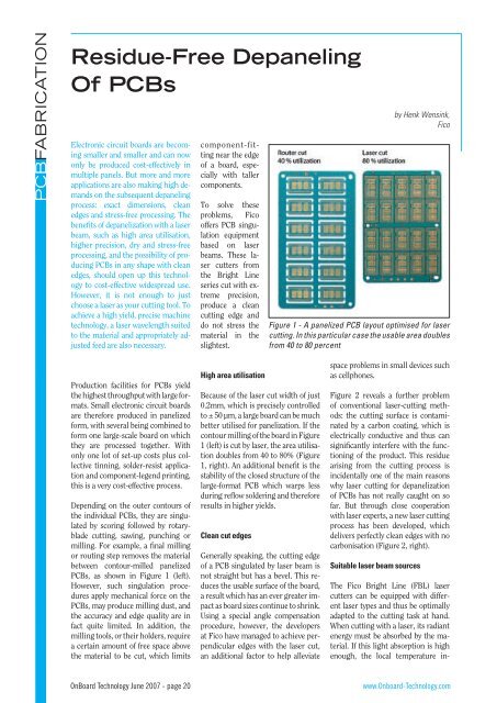
Figure 1 - A panelized PCB layout optimised for laser<br />
cutting. In this particular case the usable area doubles<br />
from 40 to 80 percent<br />
Production facilities for <strong>PCBs</strong> yield<br />
the highest throughput with large formats.<br />
Small electronic circuit boards<br />
are therefore produced in panelized<br />
form, with several being combined to<br />
form one large-scale board on which<br />
they are processed together. With<br />
only one lot of set-up costs plus collective<br />
tinning, solder-resist application<br />
and component-legend printing,<br />
this is a very cost-effective process.<br />
Depending on the outer contours of<br />
the individual <strong>PCBs</strong>, they are singulated<br />
by scoring followed by rotaryblade<br />
cutting, sawing, punching or<br />
milling. For example, a final milling<br />
or routing step removes the material<br />
between contour-milled panelized<br />
<strong>PCBs</strong>, as shown in Figure 1 (left).<br />
However, such singulation procedures<br />
apply mechanical force on the<br />
<strong>PCBs</strong>, may produce milling dust, and<br />
the accuracy and edge quality are in<br />
fact quite limited. In addition, the<br />
milling tools, or their holders, require<br />
a certain amount of free space above<br />
the material to be cut, which limits<br />
High area utilisation<br />
Because of the laser cut width of just<br />
0.2mm, which is precisely controlled<br />
to ± 50 µm, a large board can be much<br />
better utilised for panelization. If the<br />
contour milling of the board in Figure<br />
1 (left) is cut by laser, the area utilisation<br />
doubles from 40 to 80% (Figure<br />
1, right). An additional benefit is the<br />
stability of the closed structure of the<br />
large-format PCB which warps less<br />
during reflow soldering and therefore<br />
results in higher yields.<br />
Clean cut edges<br />
Generally speaking, the cutting edge<br />
of a PCB singulated by laser beam is<br />
not straight but has a bevel. This reduces<br />
the usable surface of the board,<br />
a result which has an ever greater impact<br />
as board sizes continue to shrink.<br />
Using a special angle compensation<br />
procedure, however, the developers<br />
at Fico have managed to achieve perpendicular<br />
edges with the laser cut,<br />
an additional factor to help alleviate<br />
space problems in small devices such<br />
as cellphones.<br />
Figure 2 reveals a further problem<br />
of conventional laser-cutting methods:<br />
the cutting surface is contaminated<br />
by a carbon coating, which is<br />
electrically conductive and thus can<br />
significantly interfere with the functioning<br />
of the product. This residue<br />
arising from the cutting process is<br />
incidentally one of the main reasons<br />
why laser cutting for depanelization<br />
of <strong>PCBs</strong> has not really caught on so<br />
far. But through close cooperation<br />
with laser experts, a new laser cutting<br />
process has been developed, which<br />
delivers perfectly clean edges with no<br />
carbonisation (Figure 2, right).<br />
Suitable laser beam sources<br />
The Fico Bright Line (FBL) laser<br />
cutters can be equipped with different<br />
laser types and thus be optimally<br />
adapted to the cutting task at hand.<br />
When cutting with a laser, its radiant<br />
energy must be absorbed by the material.<br />
If this light absorption is high<br />
enough, the local temperature in-<br />
<strong>OnBoard</strong> <strong>Technology</strong> June 2007 - page 20<br />
www.Onboard-<strong>Technology</strong>.com
Figure 2 - Depanelization with the Fico laser process guarantees straight edges<br />
and residue-free cutting surfaces (right) compared with conventional lasercutting<br />
procedures (left)<br />
creases to a level where the material<br />
“evaporates”. The extent to which the<br />
light is reflected or absorbed depends<br />
on the properties of the material and<br />
the wavelength of the light. CO2<br />
and YAG lasers in particular provide<br />
enough energy in different spectral<br />
ranges to make them usable for depanelization.<br />
The CO 2<br />
laser is one of the oldest laser<br />
types and has a wavelength in the<br />
infrared range of 10,600 nm. This laser<br />
technology is commonly available<br />
and provides high laser power at reasonable<br />
costs. In the FBL this laser is<br />
largely used to cut through plain PCB<br />
material and can reach cutting speeds<br />
of up to 500 mm/s for thin boards (0.2<br />
mm-thick FR4). However, a CO2 laser<br />
cannot cut through copper: because<br />
of the long wavelength of CO2 light,<br />
the strip-conductor material acts as a<br />
mirror, reflecting most of the beam.<br />
An equally widespread industrial laser<br />
source is the Nd:YAG laser (neodymium-doped<br />
yttrium aluminum garnet<br />
laser), which provides coherent light<br />
with a wavelength of 1064 nm in the<br />
near infrared range. Its laser power<br />
is less than the CO2 laser power, but<br />
is still sufficient for cutting speeds of<br />
up to 50 mm/s. Because of its shorter<br />
wavelength, its energy is also absorbed<br />
by copper, making it possible<br />
to cut through thin copper wires, for<br />
example those in BGA products. Unlike<br />
pure circuit boards, BGA products<br />
consist of several materials, such<br />
as fiber glass, epoxy, filler and copper,<br />
which all have a slightly different<br />
light absorption. Consequently, visible<br />
defects can occur, such as frayed<br />
board edges, solder mask chipping,<br />
and rough cutting edges. In addition,<br />
materials with insufficient absorption<br />
are not evaporated but merely pulverised,<br />
which can lead to the aforementioned<br />
black carbonisation. In this<br />
case, an FBL can be equipped with a<br />
cleaning system which removes the<br />
dust immediately after cutting.<br />
If the original 1064 nm wavelength<br />
of the Nd:YAG laser is not sufficiently<br />
absorbed by the material for<br />
a processing task, doubling and trebling<br />
the frequency by means of nonlinear<br />
crystals in the laser resonator<br />
very effectively produces laser beams<br />
with shorter wavelengths.<br />
Doubling the frequency produces<br />
green laser light with a wavelength<br />
of 532 nm, but with only half the<br />
power, so the cutting speed has to be<br />
reduced. However, the green light is<br />
absorbed more easily by all materials<br />
and gives a better cutting quality with<br />
less dust formation. Cosmetically,<br />
the cut looks almost perfect. Better<br />
absorption by all materials, incidentally,<br />
also means less variation in the<br />
cutting speed for black or colored<br />
compounds.<br />
By trebling the frequency of the Nd:<br />
YAG laser light, you can get a UV laser<br />
with a wavelength of 355 nm in the<br />
Figure 3 - Thin materials can be cut<br />
precisely at very high speeds<br />
ultraviolet range. Again the cutting<br />
speed is reduced but the absorption<br />
by all materials is sufficiently high to<br />
allow perfectly smooth surfaces with<br />
excellent cutting quality. However,<br />
this quality has its price.<br />
Mechanical influence<br />
At the latest at this point, it becomes<br />
clear that a compromise must be<br />
found between maximum cutting<br />
speed and cutting quality, from which<br />
an optimum laser color can then result.<br />
Furthermore, the cutting result<br />
and throughput also depend on other<br />
machine characteristics: for this reason,<br />
the laser beam and board holder<br />
of the Fico Bright Line (Figure 4)<br />
are guided and moved by high-precision<br />
linear motors. A camera system<br />
checks the exact position of the largeformat<br />
PCB so that it is positioned<br />
exactly beneath the laser beam. This<br />
results in very precise cuts with high<br />
repeatability.<br />
Figure 4 - The scope of application of the modular Fico Bright Line cutting<br />
system ranges from high-throughput depanelizer to board singulation with<br />
the highest-quality cutting edges<br />
PCBFABRICATION<br />
www.Onboard-<strong>Technology</strong>.com<br />
<strong>OnBoard</strong> <strong>Technology</strong> June 2007 - page 21