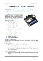
sn74lv245at octal bus transceiver with 3state outputs - CNC4PC
sn74lv245at octal bus transceiver with 3state outputs - CNC4PC
sn74lv245at octal bus transceiver with 3state outputs - CNC4PC

Create successful ePaper yourself
Turn your PDF publications into a flip-book with our unique Google optimized e-Paper software.
SCLS605A − DECEMBER 2004 − MARCH 2005<br />
absolute maximum ratings over operating free-air temperature range (unless otherwise noted) †<br />
Supply voltage range, V CC . . . . . . . . . . . . . . . . . . . . . . . . . . . . . . . . . . . . . . . . . . . . . . . . . . . . . . . . . . −0.5 V to 7 V<br />
Input voltage range, V I (see Note 1) . . . . . . . . . . . . . . . . . . . . . . . . . . . . . . . . . . . . . . . . . . . . . . . . . . −0.5 V to 7 V<br />
Voltage range applied to any output in the high-impedance<br />
or power-off state, V O (see Note 1) . . . . . . . . . . . . . . . . . . . . . . . . . . . . . . . . . . . . . . . . . . . . . . . . −0.5 V to 7 V<br />
Output voltage range applied in the high or low state, V O (see Notes 1 and 2) . . . . . . −0.5 V to V CC + 0.5 V<br />
Input clamp current, I IK (V I < 0) . . . . . . . . . . . . . . . . . . . . . . . . . . . . . . . . . . . . . . . . . . . . . . . . . . . . . . . . . . . −20 mA<br />
Output clamp current, I OK (V O < 0 or V O > V CC ) . . . . . . . . . . . . . . . . . . . . . . . . . . . . . . . . . . . . . . . . . . . . ±50 mA<br />
Continuous output current, I O (V O = 0 to V CC ) . . . . . . . . . . . . . . . . . . . . . . . . . . . . . . . . . . . . . . . . . . . . . . ±35 mA<br />
Continuous current through V CC or GND . . . . . . . . . . . . . . . . . . . . . . . . . . . . . . . . . . . . . . . . . . . . . . . . . . . ±70 mA<br />
Package thermal impedance, θ JA (see Note 3): DB package . . . . . . . . . . . . . . . . . . . . . . . . . . . . . . . . . 70°C/W<br />
(see Note 3): DGV package . . . . . . . . . . . . . . . . . . . . . . . . . . . . . . . . 92°C/W<br />
(see Note 3): DW package . . . . . . . . . . . . . . . . . . . . . . . . . . . . . . . . . 58°C/W<br />
(see Note 3): NS package . . . . . . . . . . . . . . . . . . . . . . . . . . . . . . . . . 60°C/W<br />
(see Note 3): PW package . . . . . . . . . . . . . . . . . . . . . . . . . . . . . . . . . 83°C/W<br />
(see Note 4): RGY package . . . . . . . . . . . . . . . . . . . . . . . . . . . . . . . . 37°C/W<br />
Storage temperature range, T stg . . . . . . . . . . . . . . . . . . . . . . . . . . . . . . . . . . . . . . . . . . . . . . . . . . . −65°C to 150°C<br />
† Stresses beyond those listed under “absolute maximum ratings” may cause permanent damage to the device. These are stress ratings only, and<br />
functional operation of the device at these or any other conditions beyond those indicated under “recommended operating conditions” is not<br />
implied. Exposure to absolute-maximum-rated conditions for extended periods may affect device reliability.<br />
NOTES: 1. The input and output voltage ratings may be exceeded if the input and output current ratings are observed.<br />
2. This value is limited to 5.5 V maximum.<br />
3. The package thermal impedance is calculated in accordance <strong>with</strong> JESD 51-7.<br />
4. The package thermal impedance is calculated in accordance <strong>with</strong> JESD 51-5.<br />
recommended operating conditions (see Note 5)<br />
MIN MAX UNIT<br />
VCC Supply voltage 4.5 5.5 V<br />
VIH High-level input voltage VCC = 4.5 V to 5.5 V 2 V<br />
VIL Low-level input voltage VCC = 4.5 V to 5.5 V 0.8 V<br />
VI Input voltage 0 5.5 V<br />
VO<br />
Output voltage<br />
High or low state 0 VCC<br />
3-state 0 5.5<br />
IOH High-level output current VCC = 4.5 V to 5.5 V −16 mA<br />
IOL Low-level output current VCC = 4.5 V to 5.5 V 16 mA<br />
∆t/∆v Input transition rise or fall rate VCC = 4.5 V to 5.5 V 20 ns/V<br />
TA Operating free-air temperature −40 85 °C<br />
NOTE 5:<br />
All unused inputs of the device must be held at VCC or GND to ensure proper device operation. Refer to the TI application report,<br />
Implications of Slow or Floating CMOS Inputs, literature number SCBA004.<br />
V<br />
POST OFFICE BOX 655303 • DALLAS, TEXAS 75265<br />
3