The first Transistor
The first Transistor
The first Transistor

You also want an ePaper? Increase the reach of your titles
YUMPU automatically turns print PDFs into web optimized ePapers that Google loves.
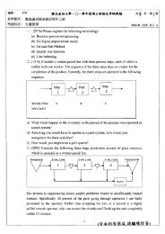
[ 半 導 體 元 件 概 論 -2009]<br />
3. 雙 極 性 接 面 電 晶 體<br />
(Bipolar Junction <strong>Transistor</strong>, BJT)<br />
王 水 進 教 授<br />
成 大 電 機 系 微 電 子 研 究 所<br />
1<br />
<strong>The</strong> <strong>first</strong> <strong>Transistor</strong><br />
[S. M. Sze, Semiconductor Device Physics and Technology, John Wiley, 1985]<br />
Emitter<br />
Collector<br />
Base<br />
2<br />
1
<strong>The</strong> discovery of the point<br />
contact transistor in 1947<br />
This work resulted in their<br />
receiving the Nobel Prize<br />
for Physics in 1956.<br />
雙 極 性 電 晶 體 發 明 人<br />
[http://www.att.com/technology/history/chronolog/47transistor.html]<br />
3<br />
典 型 BJT 封 裝<br />
[Earl D. Gates, Introduction to electronics, 4/e, Delmar, Thomson Learning Inc., 2001 ]<br />
4<br />
2
Perspective view of an oxide-isolated BJT<br />
[http://ceiba.cc.ntu.edu.tw/542U0130/u0130/electro/form6.htm]<br />
5<br />
Basic structures of BJTs<br />
[D. A. Neamen, Semiconductor Physics and Devices, IRWIN, 1997]<br />
[Encyclopedia Americana, http://go.grolier.com:80/]<br />
Conventional IC npn BJT<br />
An oxide-isolated npn BJT<br />
6<br />
3
NPN Bipolar <strong>Transistor</strong><br />
Planar junction (Bipolar) transistor<br />
Emitter<br />
Base<br />
Collector<br />
Al•Cu•Si<br />
SiO 2<br />
n p n<br />
p +<br />
+<br />
+ n-epi<br />
Electron flow<br />
n + buried layer<br />
P-substrate<br />
p +<br />
7<br />
Cross sections of BJTs<br />
[R. F. Robert, Semiconductor Device Fundamentals, Addison Wesely, 1996]<br />
A typical discrete,<br />
double-diffused pnp BJT<br />
An IC npn BJT<br />
8<br />
4
典 型 雙 極 性 接 面 電 晶 體 結 構<br />
[ 王 水 進 , 電 子 學 - 基 礎 篇 , 全 華 科 技 圖 書 ,1998]<br />
B<br />
E<br />
B<br />
垂 直 型<br />
( 縱 向 型 )<br />
n +<br />
p<br />
n<br />
n +<br />
E<br />
C<br />
B<br />
C<br />
10 20<br />
射 極<br />
n +<br />
基 極<br />
p<br />
集 極<br />
n n +<br />
水 平 型<br />
( 橫 向 型 )<br />
p +<br />
n+<br />
p n +<br />
n<br />
p +<br />
n + − 掩 埋 層<br />
SiO 2<br />
-3<br />
摻 雜 濃 度 (cm )<br />
10 18<br />
10 16<br />
p−<br />
Si基 板<br />
雜 質 分 佈 曲 線<br />
深 度<br />
9<br />
Bipolar junction transistor<br />
[From Wikipedia, the free encyclopedia]<br />
[http://en.wikipedia.org/wiki/Bipolar_junction_transistor]<br />
A bipolar (junction) transistor (BJT) is a type of transistor. It is a three-terminal<br />
device constructed of doped semiconductor material and may be used in<br />
amplifying or switching applications.<br />
Although a small part of the transistor current is due to the flow of majority<br />
carriers, most of the transistor current is due to the flow of minority carriers and<br />
so BJTs are classified as minority-carrier devices.<br />
10<br />
5
<strong>The</strong> bipolar Junction <strong>Transistor</strong>s<br />
[http://dspace.mit.edu/bitstream/handle/1721.1/36373/6-012Spring-2003/NR/rdonlyres/Electrical-Engineering-and-Computer-Science/6-<br />
012Microelectronic-Devices-and-CircuitsSpring2003/DD39CE25-C7AA-4503-999C-5E529728AE6A/0/lecture17.pdf]<br />
11<br />
Concept of<br />
<strong>Transistor</strong> Action<br />
6
雙 極 性 電 晶 體 之 基 本 操 作 :<br />
典 型 pn 接 面 於 偏 壓 下 多 數 與 少 數 載 子 之 電 通 量<br />
[ 王 水 進 , 電 子 學 - 基 礎 篇 , 全 華 科 技 圖 書 ,1998]<br />
順 偏<br />
反 偏<br />
I<br />
n +<br />
p<br />
I o<br />
p<br />
n<br />
I o<br />
I<br />
F pp<br />
>><br />
F nn<br />
F np<br />
F pn<br />
多 數 載 子 電 通 量<br />
少 數 載 子 電 通 量<br />
13<br />
雙 極 性 電 晶 體 之 基 本 操 作 :<br />
不 同 基 極 寬 度 下 由 射 極 注 入 基 極 電 子 流 之 流 動 方 向<br />
順 偏 反 偏<br />
n +<br />
p<br />
n<br />
[ 王 水 進 , 電 子 學 - 基 礎 篇 , 全 華 科 技 圖 書 ,1998]<br />
I E<br />
I C<br />
IE= IC+ IB>><br />
IB<br />
0 W<br />
I B<br />
W
Current components in a BJT<br />
[From Wikipedia, the free encyclopedia]<br />
[http://en.wikipedia.org/wiki/Bipolar_junction_transistor]<br />
15<br />
Carrier transport in a BJT<br />
[http://dspace.mit.edu/bitstream/handle/1721.1/36373/6-012Spring-2003/NR/rdonlyres/Electrical-Engineering-and-Computer-Science/6-012Microelectronic-Devices-and-<br />
CircuitsSpring2003/DD39CE25-C7AA-4503-999C-5E529728AE6A/0/lecture17.pdf]<br />
16<br />
8
Typical output characteristics of a BJT<br />
[Kwok K. Ng, Complete Guide to Semiconductor Devices, 2/e, McGraw-Hill, 2002]<br />
共 基 (CB) 組 態<br />
共 射 (CE) 組 態<br />
17<br />
<strong>Transistor</strong> (= Transfer Resistor)<br />
<br />
v I<br />
i C<br />
V CC<br />
RC<br />
i B +<br />
v CE<br />
-<br />
v O<br />
Load line<br />
V<br />
CC<br />
= i<br />
Q 1 : low resistance<br />
Q 2 : high resistance<br />
C<br />
R<br />
C<br />
+ v<br />
CE<br />
18<br />
9
Switching operation of BJT<br />
V CC<br />
i C RC<br />
i B v O<br />
v I<br />
5V<br />
0<br />
V CC<br />
0<br />
v I<br />
v O<br />
t<br />
t<br />
V<br />
R<br />
CC<br />
C<br />
C<br />
¹¡¦X<br />
B<br />
A<br />
i B<br />
I off<br />
i C<br />
V CC<br />
v CE<br />
0<br />
19<br />
[http://www.interfacebus.com/FETs.html#a]<br />
Operation <strong>The</strong>ory of<br />
BJTs<br />
10
雙 極 性 電 晶 體 之 基 本 操 作 :<br />
由 射 極 注 入 基 極 載 子 流 之 流 動 方 向<br />
[ 王 水 進 , 電 子 學 - 基 礎 篇 , 全 華 科 技 圖 書 ,1998]<br />
n p n<br />
p n p<br />
I E<br />
I C<br />
I E<br />
I C<br />
I B<br />
I B<br />
- V BE<br />
+ -V CB<br />
+<br />
+ V EB<br />
- +V BC<br />
-<br />
21<br />
Definition of BJT operation regions<br />
[S. M. Sze, Modern Semiconductor Device Physics, John Wiley, 1998]<br />
22<br />
11
Minority carrier distribution in an npn BJT<br />
[D. A. Neamen, Semiconductor Physics and Devices, IRWIN, 1997]<br />
23<br />
Carrier profiles in forward-active regime<br />
[http://dspace.mit.edu/bitstream/handle/1721.1/36373/6-012Spring-2003/NR/rdonlyres/Electrical-Engineering-and-Computer-Science/6-012Microelectronic-Devices-and-<br />
CircuitsSpring2003/DD39CE25-C7AA-4503-999C-5E529728AE6A/0/lecture17.pdf]<br />
24<br />
12
Ideal pn junction current<br />
J<br />
J<br />
p<br />
n<br />
J p<br />
(x), J n<br />
(x)<br />
-x p<br />
0<br />
x n<br />
總 電 流<br />
J p ( x n )<br />
J n (x)<br />
Jn( −xp)<br />
J p (x)<br />
Key concept<br />
= qA<br />
= qA<br />
Dp<br />
Lp<br />
Dn<br />
Ln<br />
p<br />
n<br />
no<br />
po<br />
⋅e<br />
⋅e<br />
VA<br />
/ VT<br />
VA<br />
/ VT<br />
⎫<br />
⎪<br />
⎬<br />
⎪<br />
⎭<br />
⇒<br />
J<br />
J<br />
p<br />
n<br />
N<br />
∝<br />
N<br />
A<br />
D<br />
x<br />
I = AJ = A[<br />
J<br />
Dn<br />
= qA[(<br />
n<br />
L<br />
I<br />
= I<br />
o<br />
o<br />
( e<br />
= qA[<br />
= qA[(<br />
∝ e<br />
n<br />
VA<br />
V T<br />
−<br />
−1)<br />
D<br />
L<br />
Eg<br />
kT<br />
p<br />
po<br />
n<br />
n<br />
n<br />
D<br />
L<br />
( xn)<br />
+ J<br />
Dp<br />
+ p<br />
L<br />
po<br />
n<br />
nND<br />
p<br />
+<br />
+<br />
n<br />
( −x<br />
no<br />
Dp<br />
Lp<br />
Dp<br />
L N<br />
p<br />
)( e<br />
A<br />
p<br />
p<br />
)]<br />
V A<br />
V T<br />
−1)]<br />
no<br />
]<br />
)] n ]<br />
2<br />
i<br />
25<br />
Derivation of I-V equations of BJTs<br />
x<br />
<br />
x n<br />
Eo<br />
p<br />
x x LE<br />
P n P<br />
pn( x)<br />
nx ( ) = n −Δnx ( ) e<br />
Co<br />
0 ≤ x ≤W B<br />
n<br />
−( x−xn)/<br />
LC<br />
nE ( x)<br />
n Eo<br />
− x p<br />
p Bo<br />
0<br />
W B<br />
nC ( x )<br />
− x n<br />
p Co<br />
−W<br />
/ L<br />
B B<br />
B<br />
ΔpW ( B ) − Δp( 0)<br />
e<br />
x/<br />
L ΔpW ( B ) − Δp( 0)<br />
e<br />
B<br />
px ( ) = pBo[(<br />
) e − (<br />
2 sinh( W / L )<br />
2 sinh( W / L )<br />
B<br />
B<br />
B<br />
W / LB<br />
B<br />
− x/<br />
L<br />
B<br />
) e ]<br />
27<br />
13
Derivation of I-V equations of BJTs<br />
I E = AE<br />
( J pE + J nE ) = AE<br />
[ J p ( x = 0) + J n ( x = − x p )]<br />
∂ p ( x )<br />
∂ n(<br />
x)<br />
= AE<br />
[( − q D B<br />
x = 0 ) + ( − q D E<br />
x = − x )]<br />
p<br />
∂ x<br />
∂ x<br />
q D B p Bo W<br />
= A<br />
coth ( B )[( V EB / VT<br />
E<br />
e − 1)<br />
L B L B<br />
1<br />
− ( −V<br />
BC / V<br />
q D E n EO<br />
e<br />
T − 1)] + A<br />
( V EB / VT<br />
E e − 1)<br />
W B<br />
cosh ( )<br />
L<br />
L<br />
E<br />
B<br />
I C = AC<br />
( J pC + JnC<br />
) = AC<br />
[ J p(<br />
x = WB<br />
) + Jn(<br />
x = xn)]<br />
∂ px ( )<br />
∂ nx ( )<br />
= ( − qDB x= W ) + ( −qDC x=<br />
x )<br />
∂x<br />
B<br />
∂x<br />
n<br />
−<br />
= A qD B p Bo 1 V W<br />
EB VT B VBC VT<br />
C<br />
[( e<br />
−1) −coth( )( e<br />
W<br />
L<br />
B<br />
B sinh( ) L<br />
L<br />
B<br />
B<br />
−1)]<br />
−<br />
−A C n Co VBC<br />
/ VT<br />
C ( e<br />
LC<br />
−1)<br />
28<br />
Minority carrier distribution in an npn BJT<br />
operating in the active mode<br />
[A. S. Sedra and K. C. Smith, Microelectronic Circuits, Oxford Univ. Press, 1998]<br />
Emitter<br />
(n)<br />
E-B<br />
depletion region<br />
Base<br />
(p)<br />
B-C<br />
depletion region<br />
Collector<br />
(n)<br />
n p (0)<br />
p n (0)<br />
p no<br />
n (0) = n<br />
p<br />
p (0) = p<br />
n<br />
e<br />
vBE<br />
/ VT<br />
po<br />
vBE<br />
VT<br />
noe<br />
/<br />
0<br />
I n<br />
n p (x)<br />
(ideal)<br />
n p (x)<br />
W<br />
(with recombination)<br />
I<br />
n<br />
dnp(<br />
x)<br />
= AE<br />
qDn<br />
dx<br />
np<br />
( o)<br />
= AE<br />
qDn<br />
( − )<br />
W<br />
x<br />
29<br />
14
Minority carrier distribution in an npn BJT<br />
operating in the active mode<br />
[S. M. Sze, Semiconductor Devices, Physics and Technology, John Wiley, 1985]<br />
30<br />
Minority carrier distribution in an npn BJT<br />
[D. A. Neamen, Semiconductor Physics and Devices, IRWIN, 1997]<br />
Saturation<br />
Cut-off<br />
31<br />
15
熱 平 衡 狀 態 下 BJT 之 能 帶 圖<br />
[R. F. Robert, Semiconductor Device Fundamentals, Addison Wesely, 1996]<br />
32<br />
順 向 作 用 區 工 作 電 晶 體 之 能 帶 圖<br />
結 構 示 意 圖<br />
+ −<br />
E<br />
+<br />
X E<br />
p<br />
X B<br />
n<br />
X C<br />
p<br />
I C<br />
−<br />
C<br />
能 帶 圖<br />
I E<br />
V EB<br />
電 荷 分 佈 圖<br />
V EC<br />
I B<br />
− +<br />
B<br />
V BC<br />
qV<br />
E CB qV c CE<br />
qV EB<br />
E v<br />
qN ( D − NA)<br />
N B<br />
x n<br />
− x p<br />
0 W B<br />
x<br />
N C<br />
N E<br />
33<br />
16
電 晶 體 之 能 帶 圖<br />
p<br />
n<br />
p<br />
n<br />
p<br />
n<br />
E c<br />
E c<br />
E v<br />
E v<br />
熱 平 衡<br />
狀 態<br />
E c<br />
E v<br />
E F<br />
E c<br />
E v<br />
E v<br />
qV Do<br />
E F<br />
qV Do<br />
qV D<br />
順 向 操 作<br />
狀 態<br />
E c<br />
E v<br />
E c<br />
qV CB qV CE qV qVCB<br />
EB<br />
qV CE<br />
qV EB<br />
qV D<br />
34<br />
E<br />
I B<br />
pnp 電 晶 體 之 電 流 成 份<br />
p n p<br />
I E<br />
I Ep<br />
( Ep − ICp)<br />
I Cp I C<br />
+<br />
I CBOp<br />
I En<br />
I CBOn<br />
-<br />
C<br />
I<br />
I<br />
Ep<br />
γ ≡ ≈1−<br />
E<br />
σ BW<br />
σ W<br />
E<br />
V EB<br />
Emitter efficiency<br />
α T<br />
I<br />
I<br />
Cp<br />
≡ ≈1<br />
−<br />
Ep<br />
W<br />
B<br />
E<br />
2<br />
B<br />
2<br />
p<br />
2 L<br />
-<br />
B<br />
Base transport efficiency<br />
CB SC current gain<br />
I<br />
I<br />
C<br />
α( ≡ = γα )<br />
E<br />
T<br />
+<br />
V BC<br />
IE = IEp + I En<br />
I = I + ( I − I ) − I<br />
B En Ep Cp CBO<br />
I E = I C + I B<br />
I ( = I + I )<br />
CBO CBOp CBOn<br />
I = αI + I<br />
C E CBO<br />
I = I + I = γ α I + I<br />
C Cp CBO T E CBO<br />
35<br />
17
Diffusion currents flowing in<br />
a pnp BJT under active mode biasing<br />
[R. F. Robert, Semiconductor Device Fundamentals, Addison Wesely, 1996]<br />
CB dc current gain α dc<br />
I Cp = αT<br />
I Ep = γ αT<br />
I<br />
Emitter efficiency Base transport factor<br />
E<br />
I<br />
I<br />
γ = EP<br />
ICP<br />
C = α dcIE<br />
+ ICB0<br />
= ICp<br />
+ ICn<br />
α T =<br />
IE<br />
I<br />
= γ α I + I<br />
EP<br />
T<br />
E<br />
Cn<br />
⇒<br />
α<br />
dc<br />
= γ α ,<br />
T<br />
I<br />
CB0<br />
= I<br />
Cn<br />
I<br />
C<br />
= β<br />
= α<br />
CB dc current gain β dc<br />
dc<br />
dc<br />
IB<br />
+ I<br />
( I + I<br />
C<br />
CB0<br />
B<br />
= α<br />
) + I<br />
I<br />
dc E<br />
CB0<br />
+ I<br />
CB0<br />
α dc 1<br />
IC<br />
= IB<br />
+ I<br />
1−α<br />
dc 1−α<br />
dc<br />
= β dcIB<br />
+ (1 + β dc)<br />
I<br />
α dc<br />
β dc<br />
−α<br />
dc<br />
CB0<br />
CB0<br />
36<br />
= 1<br />
37<br />
Current-Voltage Characteristics of BJTs<br />
(Gummel plot)<br />
[B. G. Streetman and S. Banerjee, Solid State Electronic Devices, Prentice Hall, 2000]<br />
High level<br />
injection<br />
Base resistance<br />
ideal<br />
ideal<br />
V EB<br />
log I C<br />
ideal<br />
37<br />
18
Gummel plot and dc current gain<br />
[R. F. Robert, Semiconductor Device Fundamentals, Addison Wesely, 1996]<br />
Ideal<br />
High-level injection,<br />
current crowding,<br />
and/or series resistance<br />
β dc<br />
V BC = 5V<br />
Ideal<br />
V EB<br />
I C<br />
(A)<br />
Data derived from a 2N2605 pnp BJT<br />
38<br />
Gummel plot: semilog plot of IC and IB vs. VBE<br />
[http://dspace.mit.edu/bitstream/handle/1721.1/36373/6-012Spring-2003/NR/rdonlyres/Electrical-Engineering-and-Computer-Science/6-<br />
012Microelectronic-Devices-and-CircuitsSpring2003/DD39CE25-C7AA-4503-999C-5E529728AE6A/0/lecture17.pdf]<br />
39<br />
19
Gummel plot of BJT (VCE = 3 V )<br />
[http://dspace.mit.edu/bitstream/handle/1721.1/36373/6-012Spring-2003/NR/rdonlyres/Electrical-Engineering-and-Computer-Science/6-012Microelectronic-Devices-and- 40<br />
CircuitsSpring2003/DD39CE25-C7AA-4503-999C-5E529728AE6A/0/lecture17.pdf]<br />
Current-Voltage<br />
Characteristics of BJTs<br />
41<br />
20
BJT 應 用 之 三 種 組 態<br />
[ 王 水 進 , 電 子 學 - 基 礎 篇 , 全 華 科 技 圖 書 ,1998]<br />
+<br />
I B<br />
V<br />
+<br />
CE<br />
V BE<br />
−<br />
I E<br />
I C<br />
−<br />
V BE<br />
+ I B<br />
−<br />
V CB<br />
V<br />
−<br />
CB<br />
I<br />
+<br />
C<br />
I E I C<br />
−<br />
+<br />
I B<br />
I E<br />
−<br />
V CE<br />
+<br />
共 射 (CE) 組 態<br />
共 基 (CB) 組 態<br />
共 集 (CC) 組<br />
42<br />
共 基 (CB) 組 態 電 晶 體 特 性<br />
I E<br />
(mA)<br />
10<br />
8<br />
6<br />
VCB = 15V<br />
VCB = 10V<br />
VCB = 5V<br />
4<br />
2<br />
0<br />
0.6 0.7 0.8 0.9<br />
V BE<br />
(Volts)<br />
I C<br />
(mA)<br />
10<br />
8<br />
6<br />
4<br />
2<br />
IE = 10 mA<br />
IE = 8 mA<br />
IE = 6 mA<br />
IE = 4 mA<br />
IE = 2 mA<br />
I CBO<br />
IE = 0 mA<br />
0 1 2 3 4 5 6<br />
VBE ( Volts)<br />
I E I C<br />
I B I B<br />
I E I C<br />
−<br />
V BE<br />
+<br />
+<br />
V CB<br />
−<br />
+<br />
V EB<br />
−<br />
−<br />
V BC<br />
+<br />
43<br />
21
共 射 (CE) 組 態 電 晶 體 特 性<br />
3<br />
20<br />
18<br />
16<br />
I B =100 uA<br />
I B<br />
(μA)<br />
2<br />
1<br />
VCE = 5V<br />
VCE = 15V<br />
I C (mA)<br />
14<br />
12<br />
10<br />
8<br />
6<br />
80 uA<br />
60 uA<br />
40 uA<br />
4<br />
20 uA<br />
0 04 . 06 . 08 . 10 . 12 . 14 .<br />
VBE ( Volts)<br />
2<br />
0 uA<br />
0<br />
0.0 0.5 1.0 1.5 2.0 2.5 3.0 3.5 4.0<br />
V CB (V)<br />
I C<br />
I C<br />
I B<br />
+<br />
+<br />
V CE<br />
V BE −<br />
I<br />
−<br />
E<br />
−<br />
V EB<br />
+<br />
I B<br />
I E<br />
−<br />
V EC<br />
+<br />
44<br />
Typical output characteristics of a BJT<br />
[Kwok K. Ng, Complete Guide to Semiconductor Devices, 2/e, McGraw-Hill, 2002]<br />
共 基 (CB) 組 態<br />
共 射 (CE) 組 態<br />
45<br />
22
共 集 (CC) 組 態 電 晶 體 特 性<br />
I B (mA)<br />
20<br />
18<br />
15<br />
13<br />
V CB = 5 V<br />
V CB = 10 V<br />
V CB = 15 V<br />
10<br />
8<br />
5<br />
3<br />
0<br />
0 2 4 6 8 10 12 14 16<br />
V CB (V)<br />
I E (mA)<br />
20<br />
18<br />
16<br />
14<br />
12<br />
10<br />
8<br />
6<br />
4<br />
2<br />
IB = 100 μ A<br />
80 μA<br />
60 μA<br />
40 μA<br />
20 μA<br />
0 μA<br />
0<br />
0.0 0.5 1.0 1.5 2.0 2.5 3.0 3.5 4.0<br />
V CE (V)<br />
I E<br />
I E<br />
−<br />
V BC<br />
+<br />
I B<br />
I C<br />
−<br />
V CE<br />
+<br />
+<br />
I B<br />
V BC I −<br />
+<br />
−<br />
C<br />
V EC<br />
46<br />
Figure-of-Merit (FOM) for BJT performance<br />
[S. M. Sze, Modern Semiconductor Device Physics, John Wiley, 1998]<br />
Current gain cutoff frequency, f T<br />
<strong>The</strong> frequency at which the short-circuit current gain (h fe<br />
, or β) drop to<br />
unity.<br />
A key estimator of transistor high-speed performance<br />
1<br />
wc<br />
( kT / q)<br />
= τ b + τ e'<br />
+ + ( RE<br />
+ RC<br />
) CBC<br />
+ ( CBE<br />
+ CBC<br />
)<br />
2π fT<br />
2vs<br />
IC<br />
Maximum frequency of oscillation, f max<br />
<strong>The</strong> frequency at which the maximum available power gain (MAG) of<br />
the transistor drops to unity.<br />
F max<br />
is different from (and typically larger than) f T<br />
, because in<br />
addition to current gain, f max<br />
takes into account the possibility of<br />
voltage gain.<br />
fmax 2 1 Re( Zin)<br />
2<br />
G p = ( ) = [ ] h fe<br />
f 4 Re( Zout<br />
)<br />
T 1/ 2<br />
max ( )<br />
8π RBCBC<br />
f =<br />
f<br />
Figure of Merit: 效 益 指 數 、 評 量 指 標<br />
47<br />
23
Figure-of-Merit for BJT performance<br />
[S. M. Sze, Modern Semiconductor Device Physics, John Wiley, 1998]<br />
48<br />
Non-ideal effects of BJTs<br />
49<br />
24
BJT 之 穿 透 崩 潰 (punch-through breakdown)<br />
W B<br />
E<br />
N + P N<br />
C<br />
punch-through<br />
breakdown voltage<br />
Depletion<br />
region<br />
B<br />
V<br />
2<br />
PT B B s<br />
( = qN W / 2ε )<br />
W B<br />
V B<br />
E<br />
N + P N<br />
B<br />
Depletion<br />
region<br />
C<br />
ΔV B<br />
發 生 穿 透 崩 潰 時<br />
V + V<br />
bi CB<br />
E c<br />
E c<br />
50<br />
電 晶 體 與 兩 端 間 之 崩 潰 曲 線 ( 第 三 端 開 路 )<br />
I<br />
1<br />
M =<br />
V<br />
1 − ( )<br />
I CEO<br />
BV CBO<br />
m<br />
I<br />
CEO<br />
BV CEO<br />
I CBO<br />
BV CBO<br />
1/ m<br />
β<br />
I CBO<br />
=<br />
1−α<br />
M<br />
V<br />
BV<br />
CEO<br />
= BV<br />
BV<br />
≈<br />
CBO<br />
CBO<br />
(1−<br />
α)<br />
I B = 0<br />
I CEO<br />
I CBO<br />
I E = 0<br />
1/ m<br />
51<br />
25
<strong>The</strong> avalanche breakdown in a transistor<br />
[B. G. Streetman and S. Banerjee, Solid State Electronic Devices, Prentice Hall, 2000]<br />
52<br />
Carrier multiplication and feedback mechanism<br />
[R. F. Robert, Semiconductor Device Fundamentals, Addison Wesely, 1996]<br />
0: initial hole injection<br />
1: injected hole entering the CB<br />
depletion junction<br />
2: e-h pair generation by impact ionization<br />
3: generated electrons being swept<br />
into the vase<br />
4: excess base electrons injected<br />
into the emitter<br />
5: hole injected from the emitter<br />
into the base in response to the<br />
step 4 electron injection<br />
53<br />
26
Non-ideal I-V characteristics of BJTs<br />
[R. F. Robert, Semiconductor Device Fundamentals, Addison Wesely, 1996]<br />
Non Early effect<br />
no carrier multiplication<br />
With Early effect and<br />
carrier multiplication<br />
With Early effect<br />
no carrier multiplication<br />
54<br />
<strong>The</strong> Early effect<br />
[B. G. Streetman and S. Banerjee, Solid State Electronic Devices, Prentice Hall, 2000]<br />
55<br />
27
Dependence of i C on the collector voltage –<br />
the Early effect<br />
[A. S. Sedra and K. C. Smith, Microelectronic Circuit, Oxfor Univ. Press, 1998]<br />
i<br />
C<br />
v<br />
/ CE<br />
= I v V<br />
Se<br />
BE T (1 + ) Output resistance<br />
V<br />
A<br />
⎡ ∂i<br />
ro<br />
≡ ⎢<br />
⎣∂v<br />
C<br />
CE<br />
vBE<br />
=const.<br />
⎤<br />
⎥<br />
⎦<br />
−1<br />
56<br />
Geometrical effect-<br />
current crowding<br />
Emitter area ≠ collector area<br />
Bulk and contact resistance<br />
(using thin epilayer or heavily doped buried layer)<br />
57<br />
28
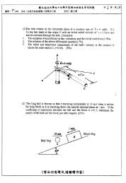
Current crowding<br />
58<br />
Cross section of a BJT under active bias<br />
C-B<br />
space-charge<br />
layer<br />
Collector region<br />
Lines of flow of<br />
majority carriers<br />
<strong>The</strong> base current is supplied form two side base contact and flows<br />
toward the center of the emitter causing the BE voltage drop to vary<br />
with position.<br />
62<br />
29
Base resistance<br />
Extrinsic base resistance<br />
ρBX<br />
L ρBX<br />
d<br />
R1<br />
= =<br />
A ( x + x ) W<br />
E<br />
B<br />
Intrinsic base resistance<br />
R<br />
2<br />
ρBIh<br />
=<br />
3x<br />
W<br />
B<br />
Base resistance<br />
R = r<br />
b<br />
= RC<br />
+ R1<br />
+ R2<br />
x<br />
63<br />
Effect of Base Resistance<br />
[B. G. Streetman and S. Banerjee, Solid State Electronic Devices, Prentice Hall, 2000]<br />
64<br />
30
An interdigitated geometry<br />
to release the effects of emitter current crowding<br />
[B. G. Streetman and S. Banerjee, Solid State Electronic Devices, Prentice Hall, 2000]<br />
top view of<br />
implanted region<br />
65<br />
Geometry design of power BJTs<br />
66<br />
31
<strong>Transistor</strong> collector resistance R CS<br />
In active region<br />
the collector junction is reveres biased<br />
and hence represents a rather high<br />
impedance. <strong>The</strong> collector voltage<br />
drop I C<br />
R CS<br />
is normally small<br />
compared to the collector junction<br />
resistance and can be neglected.<br />
In saturation region<br />
<strong>The</strong> collector junction is forward biased, the collector bulk voltage drop<br />
generally even exceeds the potential drop across the junction.<br />
<strong>The</strong> effect is most pronounced at low CE voltages where the BJT<br />
is in saturation and hence is collecting minority carrier inefficiently<br />
(the collector is back injection to the emitter).<br />
67<br />
Emitter-collector shorts caused by diffusion pipes or spikes<br />
through the base along the dislocations<br />
Diffusion pipes<br />
Diffusion spikes<br />
Dislocations:<br />
oxidation induced stacking faults, epitaxial-growth-induced<br />
slip dislocations, and other process-induced defects<br />
68<br />
32