
You also want an ePaper? Increase the reach of your titles
YUMPU automatically turns print PDFs into web optimized ePapers that Google loves.
7. <br />
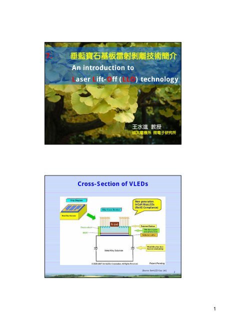
An introduction to<br />
<strong>Laser</strong> <strong>Lift</strong>-Off (LLO) technology<br />
<br />
<br />
1<br />
Cross-Section of VLEDs<br />
[Source: SemiLED Cop. Ltd.]<br />
2<br />
1
Wafer bonding Technology<br />
3<br />
Transient-liquid-phase bonding<br />
4<br />
2
Bonding and transfer process<br />
5<br />
X-ray diffraction of transferred GaN<br />
6<br />
3
Pattern transfer by LLO<br />
7<br />
<strong>Laser</strong> <strong>Lift</strong>-<strong>off</strong> technology<br />
8<br />
4
[William S. Wong, Michael Kneissl, David W. Treat, Mark Teepe,<br />
Naoko Miyashita, and Noble M. Johnson Electronic Materials Laboratory<br />
XEROX Palo Alto Research Center E-mail:wswong@parc.xerox.com]<br />
10<br />
5
11<br />
Schematic view of the laser lift<strong>off</strong> (LLO) process<br />
High intensity laser pulses enter<br />
the sample via the sapphire<br />
substrate and thermally<br />
decompose a thin GaN-layer at<br />
the substrate interface.<br />
The shock waves resulting from<br />
the explosive production of<br />
nitrogen gas during each laser<br />
pulse are damped by placing the<br />
GaN-sample into sapphire<br />
powder.<br />
A hot plate can be used to raise<br />
the substrate temperature during<br />
the process, in order to relieve<br />
some of the accumulated thermal<br />
strain.<br />
12<br />
6
A simulated temperature profile as a<br />
function of time and depth<br />
By solving the one- imensional heat equation, the extent of interaction at the<br />
GaN/sapphire interface with a pulsed UV-laser is found to be highly localized to<br />
the thin film/substrate interface.<br />
For a single 38 ns,<br />
600 mJ/cm 2 incident pulse from a<br />
KrF laser<br />
The numerical solution to the onedimensional<br />
heat equation assumes<br />
a semiinfinite slab in the sapphire<br />
and GaN region.<br />
<strong>Laser</strong>-induced heating<br />
14<br />
7
Enhancing microsystem functionality<br />
through materials integration<br />
15<br />
Approach to integration<br />
16<br />
8
Approach to integration<br />
17<br />
Free-standing InGaN LEDs<br />
18<br />
9
Cross sectional SEM micrograph of a<br />
transferred GaN film onto a Si substrate<br />
GaN on Si by Pd-In bonding and<br />
laser lift-<strong>off</strong> (LLO)<br />
GaN LED on Si<br />
200 μm<br />
Pd-In metal bilayers were used as bonding material which formed the<br />
compound PdIn3 after the low-temperature bonding process.<br />
Cleaving the Si substrate was performed to make the cleavage facets on<br />
the GaN.<br />
InGaN LEDs on Si Substrates<br />
20<br />
10
LLO integration process<br />
21<br />
Cleaved mirror facets<br />
22<br />
11
Continuous wave InGaN LDs on Cu<br />
23<br />
Continuous wave InGaN LDs on Cu<br />
24<br />
12
CW laser diodes on diamond<br />
25<br />
Improved output performance<br />
26<br />
13
<strong>Laser</strong> <strong>Lift</strong>-<strong>off</strong> <strong>Process</strong><br />
27<br />
<strong>Laser</strong> lift-<strong>off</strong> process<br />
E g : E 0 > E 1 > hν> E 2 > E 3<br />
hν<br />
Sapphire<br />
Buffer Layer<br />
N-GaN<br />
E c<br />
E 0 E 1 E 2 E 3<br />
E v<br />
Undoped GaN<br />
脈 衝 雷 射 被 吸 收 處<br />
AlN<br />
28<br />
14
<strong>Laser</strong> lift-<strong>off</strong> (LLO) technique<br />
Thermal decomposition of an interfacial layer induced by<br />
pulse irradiation of KrF (248nm) excimer laser<br />
Only interfacial layer of GaN reach high temperature<br />
<strong>Laser</strong> beam<br />
Sapphire(Al 2 O 3 )<br />
Buffer<br />
layer<br />
M.Q.W.<br />
p-GaN<br />
Sapphire(Al 2 O 3 )<br />
n-GaN<br />
(E g ≈ 9eV)<br />
(E g =3.4eV)<br />
GaN<br />
(900ºC~1000ºC) C)<br />
Δ<br />
n-GaN<br />
Ga + ½ N 2<br />
Ni<br />
Ni<br />
29<br />
The excimer laser system<br />
Light intensity<br />
Time<br />
The schematic diagram of KrF ecximer laser<br />
<strong>Laser</strong> medium<br />
Wavelength<br />
Maximum pulse energy<br />
Maximum laser fluence<br />
Full-Width-Half-Magnitude<br />
Pulse repetition rate<br />
KrF<br />
248 nm<br />
380~400 mJ/pulse<br />
2000 mJ/cm 2<br />
30 ns<br />
1~100 Hz<br />
Excimer <strong>Laser</strong> Micro-Machining System<br />
(Excitech PS-2000)<br />
35<br />
15
<strong>Laser</strong> lift-<strong>off</strong> (LLO) process<br />
<strong>Laser</strong> fluence : 850 mJ/cm 2<br />
<strong>Laser</strong> pulse time : 38 ns<br />
E<br />
1.24<br />
=<br />
λ<br />
1.24<br />
0.248<br />
g<br />
= =<br />
C<br />
5 eV<br />
Sapphire<br />
Sapphire(Al 2 O 3 )<br />
400 μm<br />
Buffer layer<br />
(u-GaN)<br />
M.Q.W.<br />
p-GaN<br />
n-GaN<br />
GaN<br />
(900ºC~1000ºC)<br />
∆<br />
Ga + ½ N 2<br />
Oxidized Ni/Au<br />
& Ti/Al/Ti/Au<br />
Ni substrate<br />
80 μm<br />
[W. S. Wong, et al., APL,<br />
pp. 599-601, 1998]<br />
36<br />
KrF<br />
Copper mask: 1cm×1 cm<br />
<strong>Laser</strong> beam<br />
A block size after laser beam through<br />
z<br />
the lens (10×): 1 mm×1 mm<br />
Reactive energy density:<br />
10 倍 聚 焦 鏡<br />
y<br />
850-1000 mJ/cm 2<br />
• Scanning velocity:<br />
能 量 強<br />
500-800 mm/min<br />
Z=0 mm<br />
Pattern LLO 加 工 區 ( 聚 焦 面 )<br />
5 mm<br />
x<br />
Z= -3.74 mm<br />
能 量 弱<br />
整 面 LLO 加 工 區<br />
GaN wafer<br />
投 影 片<br />
金 屬 加 工 平 台<br />
-3.74 mm,0.1 mm,<br />
wafer2D<br />
38<br />
16
-<br />
0.5 mm<br />
Start<br />
0.5 mm<br />
0.5 mm<br />
<strong>Laser</strong> beam size<br />
1 mm<br />
2-inch wafer<br />
1 mm<br />
End<br />
: Overlap for neighboring laser pulse<br />
39<br />
-<br />
(overlap)<br />
y 軸 移 動 0.3 mm 打 一 發<br />
0.3 mm<br />
Sample<br />
X 軸 移 動 0.3 mm 打 一 發<br />
<strong>Laser</strong> beam size<br />
1 mm<br />
1 mm<br />
雷 射 移 動 的 方 向<br />
40<br />
17
Patterned LLO technology<br />
[Patent: I287309(ROC)]<br />
<strong>Laser</strong> Beam<br />
Mask<br />
Patterned<br />
<strong>Laser</strong> Beam<br />
300×300, 230×230 1000×1000<br />
S. J. Wang et al., Appl. Phys. Letts, vol. 87, 2005<br />
360×360, 90 ×90 unit: μm 2<br />
S. L. Chen et al., IEEE Photon. Technol. Lett, vol. 19,<br />
41<br />
2007<br />
unit: μm 2<br />
Die size: 300 × 300 μm 2<br />
Die size: 1000 × 1000 μm 2<br />
42<br />
18
46<br />
47<br />
19
48<br />
The luminous efficiency and total output power of dichromatic<br />
white LEDs with injection currents from 5 to 50 mA<br />
49<br />
20
50<br />
53<br />
21
Substrates for III-nitride heteroepitaxy: a brief survey<br />
Standard vapor phase epitaxy methods for GaN growth (HVPE,<br />
MOCVD),<br />
high growth temperatures (>1000 °C)<br />
high concentration of ammonia and hydrogen<br />
considerably reduce the choice of possible substrates.<br />
For device production on an industrial scale, the substrate has to fulfill further<br />
criteria such as minimum size (2”), atomically flat surfaces, and availability in<br />
large quantities at an acceptable price.<br />
Sapphire was and still is the most common substrate for the deposition of<br />
GaN-based light-emitting diodes (LEDs), because of its reasonably low cost<br />
and wide availability, and despite the fact that it has a large lattice constant<br />
and thermal expansion coefficient mismatch with respect to GaN.<br />
54<br />
57<br />
22
Thermally induced decomposition<br />
of GaN and the corresponding flux of nitrogen<br />
from the GaN surface using a heating rate of 0.3 K/s<br />
The flux of nitrogen molecules,<br />
Φ(N2), leaving the crystal surface in<br />
vacuum shows an exponential<br />
increase with temperature above<br />
830 °C, which can be parametrized<br />
as:<br />
61<br />
Effect of a single shot from a Nd:YAG-laser on the<br />
optical appearance of a GaN layer on sapphire<br />
Effect of a single shot from a<br />
Nd:YAG-laser on the optical<br />
appearance of a GaN layer on<br />
sapphire. For absorbed energy<br />
densities below 200 mJ/cm2, no<br />
visible effects can be observed.<br />
For energy densities above the<br />
sublimation threshold of approx. 250<br />
mJ/cm2, the entire surface of the<br />
GaN epilayer is transformed into<br />
metallic Ga, giving rise to the dark<br />
colour in the upper half of the<br />
specimen pictures.<br />
Close to the sublimation threshold,<br />
inhomogeneities of the intensity<br />
profile of the laser beam are clearly<br />
visible in the irradiation patterns.<br />
62<br />
23
Experimentally determined decomposition depth caused by<br />
a single pulse of a Nd:YAG laser in GaN at room<br />
temperature as a function of the pulse intensity absorbed in<br />
the thin GaN layer on sapphire.<br />
The energy density of the laser shots<br />
should be kept as close as possible<br />
to the threshold value necessary for<br />
GaN decomposition. Any additional<br />
energy will lead to unwanted thermal<br />
and mechanical stress which can<br />
favour film spalling and peel-<strong>off</strong> after<br />
sapphire removal.<br />
The change in slope for pulse intensities exceeding 350 mJ/cm2 is probably<br />
due to absorption or reflection of the laser light by the metallic Ga layer formed 63<br />
during the process.<br />
Dependence of the laser-induced etch depth of GaN<br />
on the number of laser pulses with and without the<br />
presence of HCl-vapor<br />
The laser treatment was performed at 300 K with an absorbed pulse intensity of<br />
290 mJ/cm2 and a pulse repetition rate of 10 Hz. From the slope of the straight<br />
64<br />
line an average etch rate of 330 nm/s can be deduced.<br />
24
Comparison between the maximal etch rates for GaN<br />
achieved by laser- nduced etching and conventional<br />
reactive ion etching methods<br />
ICP: inductively coupled plasma<br />
MIE: magnetron ion etching<br />
CAIBE: chemically assisted ion<br />
beam etching<br />
ECR: electron cyclotron resonance<br />
RIE: reactive ion etching<br />
Using laser-induced thermal decomposition of GaN, much higher etch rates in<br />
the range of 1 μm/s can be realized.<br />
65<br />
Temporal and spatial variation of the temperature at the sapphire/GaN interface<br />
(depth zero) during and after a Nd:YAG laser pulse (left figure, λ = 355 nm, τ = 6<br />
ns, I = 300 mJ/cm2) and a KrF excimer laser pulse (right figure, λ = 248 nm, τ =<br />
38 ns, I = 600 mJ/cm2).<br />
The intensities of the two pulses were chosen such as to obtain the same<br />
maximum temperature of 1100 K (sublimation temperature, cf. Fig. 2).<br />
66<br />
25
Because of the much longer pulse duration in the case of the KrF laser, a<br />
higher pulse energy of typically 600 mJ/cm2 is necessary to heat the GaN<br />
above the sublimation threshold, whereas pulse energies of 300 mJ/cm2 are<br />
sufficient in the case of the Nd:YAG laser.<br />
Since optical thermalization and relaxation processes in GaN occur on a much<br />
faster timescale of ps or a few ns, the temperature profiles generated by the<br />
different laser pulses can be calculated quite easily in a one-dimensional<br />
model based on the temporal shape of the laser pulse, the known absorption<br />
coefficients of GaN, and the thermal properties ( heat capacitance and<br />
conductivity) of GaN and sappire.<br />
67<br />
Photograph of a 275 μm thick free-standing GaN<br />
film, after removal from the 2” sapphire substrate<br />
The missing pieces at the wafer border actually had broken <strong>off</strong> right after the<br />
HVPE growth.<br />
68<br />
26
Experimental results<br />
Image of a HVPE-GaN sample with an area of about 1 cm 2 and a thickness of<br />
30 μm fixed with epoxy resin to a glass holder after laser lift-<strong>off</strong><br />
The delaminated sapphire substrate is shown on the left.<br />
69<br />
<strong>Process</strong> sequence for the laser lift-<strong>off</strong> of 2” GaN<br />
membranes<br />
a) <strong>Laser</strong> lift-<strong>off</strong> of the GaN film covered with silicone<br />
elastomer and mounted onto a support;<br />
b) Sapphire removal after laser scanning;<br />
c) Deposition of a ∼3 μm thick layer of thermoplastic<br />
adhesive at 120 °C;<br />
d) Peel-<strong>off</strong> of the silicone elastomer.<br />
Subsequently, the GaN film can be easily isolated by dissolving the<br />
thermoplastic adhesive in an acetone bath.<br />
70<br />
27
<strong>Process</strong> flow for bonding and transfer<br />
71<br />
Experimental results<br />
Delaminated 3 μm thick 2” GaN film (not structured) wafer-bonded onto GaAs<br />
(left) and the corresponding GaN-free sapphire substrate (right)<br />
The transferred GaN film is essentially defect free, except for some peeled<strong>off</strong><br />
areas at the wafer rim.<br />
72<br />
28
Summary and conclusions<br />
The present state-of-the-art concerning the laser-induced lift-<strong>off</strong> of both thin<br />
and thick GaN films and heterostructures from sapphire substrates has been<br />
reviewed.<br />
The physical background of the laserinduced thermal decomposition of GaN by<br />
short intense pulses of KrF excimer lasers and the third harmonic of Nd:YAG<br />
lasers is discussed, and potential applications for rapid etching of GaN have<br />
been outlined.<br />
Of particular interest for future applications is the possibility to produce<br />
freestanding GaN films by laser lift-<strong>off</strong> of heteroepitaxial layers from transparent<br />
sapphire substrates.<br />
Specific applications include the production of freestanding GaN<br />
pseudosubstrates starting from thick HVPE grown epilayers, as well as the<br />
delamination of thin GaN device heterostructures for the purpose of wafer<br />
bonding onto foreign substrates or for flip-chip bonding in device technology.<br />
73<br />
Summary and conclusions<br />
Using optimized processes, the defect free lift-<strong>off</strong> of entire 2” wafers can be<br />
achieved for GaN film thicknesses ranging from 3 to 300 μm.<br />
Separation of thin device heterostructures from their sapphire substrates opens<br />
up new possibilities for the formation of electrical contacts, the extraction of<br />
photons, and for thermal management.<br />
Thick GaN films grown by HVPE can be removed from their sapphire<br />
substrates to obtain freestanding GaN pseudosubstrates for the homoepitaxial<br />
growth of high quality epilayers.<br />
The required processing steps, including surface preparation after laser lift-<strong>off</strong>,<br />
have been described and the structural and optoelectronic properties of<br />
homoepitaxial GaN layers deposited on freestanding pseudosubstrates have<br />
been investigated.<br />
All results suggest that the laser lift-<strong>off</strong> method may become a major technique<br />
in future III-nitride device technology.<br />
74<br />
29
75<br />
Schematic diagram of the YAG-LED and KrF-LED<br />
transfer process<br />
76<br />
30
77<br />
78<br />
31
79<br />
For higher intensities, the absorbed photon energy leads to local heating of<br />
the layer and causes the destruction of the GaN.<br />
Only those devices with median energy densities approximately 800<br />
mJ/cm2 for KrF laser and 200 mJ/cm2 for YAG laser have good yields 90%.<br />
Under a reverse bias of −5 V, the leakage current of YAG-LED was 1.65103<br />
nA, which was 10 000 times higher than that of the KrF-LED 0.17 nA.<br />
These degradations were caused by the laser lift-<strong>off</strong> processes, which<br />
generated the screw dislocations. The screw dislocation density penetrated<br />
through MQW region of YAG-LED was 2.9109 cm−2, which was ten times<br />
higher than that of the KrF-LED 3.75108 cm−2.<br />
This is because the absorption coefficient of GaN at 248 nm for KrF-LED is<br />
2105 cm−1, which is 3.33 times higher than that at 355 nm for YAG-LED.<br />
80<br />
32
81<br />
<strong>Process</strong> flow for bonding and transfer of InGaN SQW LED<br />
from sapphire onto Si<br />
82<br />
33
Starting material—prefabricated InxGa12xN SQW LED/sapphire and Si<br />
supporting substrate; deposit Pd–In bilayer on InxGa12xN device layer and Pd<br />
on receptor Si substrates;<br />
(2) Bond InxGa12xN SQW LED/sapphire onto Si supporting substrate,<br />
(3) KrF laser irradiation of the sapphire/InxGa12xN SQW LED/PdIn3 /Si<br />
structure through the transparent sapphire substrate;<br />
(3) Heat post laser-processed structure above melting point of Ga to release<br />
sapphire substrate; and<br />
(4) CAIBE etch to isolate device and deposition of n-contact metal. The inset<br />
shows InxGa12xN SQW structure after LLO and metal contact definition.<br />
83<br />
<strong>Process</strong> flow for bonding and transfer of InGaN SQW LED<br />
from sapphire onto Si<br />
84<br />
34
Room-temperature dc I –V characteristics for a typical 250mm<br />
3250mm InxGa12xN SQW LED on Si<br />
Photograph of a functioning InxGa12xN SQW blue LED on Si.<br />
The LED shows no dark-line features due to microcracking from either the<br />
LLO process or the thermal expansion coefficient mismatch between GaN<br />
and Si.<br />
85<br />
Schematic diagram of the nano-roughed LED structure<br />
86<br />
35
The schematic diagram of<br />
laser etching process setup<br />
87<br />
SEM and AFM images of the Ni nano-mask on p-GaN<br />
surface morphology of a nano-roughened LED sample<br />
88<br />
36
Forward I–V curves and Room temperature EL spectra<br />
of conventional and nano-roughened LEDs*<br />
* with laser etching energy of 300 mJ/cm2 at a current of 20mA<br />
89<br />
[IEEE PTL Vol. 29, No. 3, 2008]<br />
91<br />
37
[IEEE PTL Vol. 29, No. 3, 2008]<br />
92<br />
[IEEE PTL Vol. 29, No. 3, 2008]<br />
93<br />
38
I–V characteristics of chemically lifted <strong>off</strong><br />
vertical LED<br />
[IEEE PTL Vol. 29, No. 3, 2008]<br />
94<br />
Thank You!<br />
2007/10/29<br />
96<br />
39