- Page 1 and 2: AR8327/AR8327N Seven-port Gigabit E
- Page 3 and 4: Table of Contents General Descripti
- Page 5 and 6: 3.5.17 PORT4_VLAN_CTRL1 ...........
- Page 7 and 8: 3.7.121 ACL_RATE_CTRL0_18 .........
- Page 9 and 10: 6 Ordering Information ............
- Page 11 and 12: Revision History Table 0-1. AR8161-
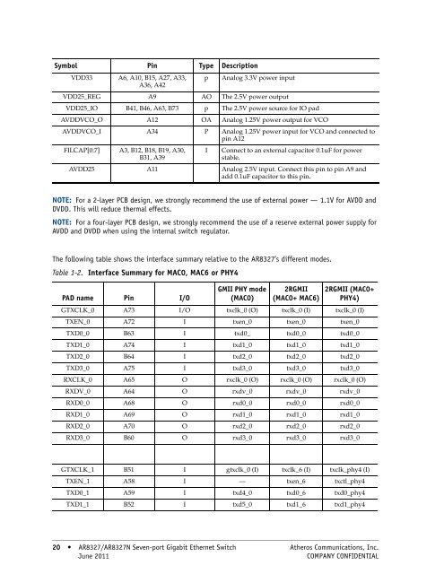
- Page 13 and 14: 1. Pin Descriptions This section co
- Page 15 and 16: B 1 A 3 B 19 A 20 A 86 B 76 B 20 A
- Page 17 and 18: Table 1-1. Signal to Pin Relationsh
- Page 19: Table 1-1. Signal to Pin Relationsh
- Page 23 and 24: 2. Functional Description The AR832
- Page 25 and 26: Table 2-1. Atheros Header Type 5'h1
- Page 27 and 28: duplex flow control mode is not set
- Page 29 and 30: Table 2-6. Action Definition 41 CTA
- Page 31 and 32: Table 2-9. IPv4 Pattern 15 [7:6] RE
- Page 33 and 34: Table 2-13. IPv6 Pattern — Patter
- Page 35 and 36: 2.7.7 Enhanced MAC Pattern Table 2-
- Page 37 and 38: 2.9 LED Control There are totally 6
- Page 39 and 40: Mode is checking if the ingress VID
- Page 41 and 42: 2.10.9 VLAN Table The AR8327 suppor
- Page 43 and 44: Table 2-29. Application Cases 1 and
- Page 45 and 46: Table 2-30. MIB Counters (continued
- Page 47 and 48: 2.17.3 Forwarding Unknown The AR832
- Page 49 and 50: Table 2-32. Bit Name Description 63
- Page 51 and 52: Table 2-34. Basic NAT Table 73:72 A
- Page 53 and 54: 2.19.4 ARP ENTRY The HNAT module su
- Page 55 and 56: 2.21 Memory Map Table 2-38. Memory
- Page 57 and 58: 3. Register Descriptions Table 3-1
- Page 59 and 60: 3.2.1 MASK_CTRL Address: 0x0000 HW
- Page 61 and 62: Table 3-6 summarizes the PORT5 PAD
- Page 63 and 64: Table 3-7. PORT6 PAD MODE CTRL Regi
- Page 65 and 66: Table 3-9. Global Interrupt Registe
- Page 67 and 68: Table 3-11. Global Interrupt Mask R
- Page 69 and 70: Table 3-14 summarizes the MIB Funct
- Page 71 and 72:
Table 3-17 summarizes the BIST_CTRL
- Page 73 and 74:
Table 3-21 summerizes LED_CTRL1 Reg
- Page 75 and 76:
SFT&HW RST Table 3-26 summarizes th
- Page 77 and 78:
Table 3-28. Port 1 Status Register
- Page 79 and 80:
Table 3-30. Port 3 Status Register
- Page 81 and 82:
Table 3-32. Port 5 Status Register
- Page 83 and 84:
Table 3-35. PORT 0 Header Control R
- Page 85 and 86:
3.2.36 PORT4_HEADER_CTRL Address 0x
- Page 87 and 88:
Table 3-42 summarizes the SGMII_CTR
- Page 89 and 90:
3.3 EEE CTRL REGISTER SUMMARY (Addr
- Page 91 and 92:
Table 3-48. PORT 2 EEE Variable Reg
- Page 93 and 94:
Table 3-54. PORT 4 EEE Variable Reg
- Page 95 and 96:
3.4 PARSER REGISTER SUMMARY(Address
- Page 97 and 98:
Bit R/W Inital Value Mnemonic Descr
- Page 99 and 100:
Table 3-64. Frame Ack Control Regis
- Page 101 and 102:
Bit R/W Inital Value Mnemonic Descr
- Page 103 and 104:
3.4.9 WIN_RULE_CTRL3 Address 0x0224
- Page 105 and 106:
Table 3-72. Window Rule Control Reg
- Page 107 and 108:
Table 3-76. Window Rule Control Reg
- Page 109 and 110:
3.5 ACL REGISTER (Address Range: 0x
- Page 111 and 112:
Table 3-86. ACL Function Register 4
- Page 113 and 114:
Bit R/W Inital Value Mnemonic Descr
- Page 115 and 116:
Bit R/W Inital Value Mnemonic Descr
- Page 117 and 118:
SFT&HW RST Table 3-95 summarizes th
- Page 119 and 120:
3.5.17 PORT4_VLAN_CTRL1 Address 0x0
- Page 121 and 122:
Bit R/W Inital Value Mnemonic Descr
- Page 123 and 124:
Table 3-103 summarizes the IPv6 Pri
- Page 125 and 126:
3.6.1 ATU_DATA0 Address 0x0600 SFT&
- Page 127 and 128:
Table 3-110. ATU_FUNC_REG Register
- Page 129 and 130:
Bit R/W Inital Value Mnemonic Descr
- Page 131 and 132:
Bit R/W Inital Value Mnemonic Descr
- Page 133 and 134:
Bit R/W Inital Value Mnemonic Descr
- Page 135 and 136:
Bit R/W Inital Value Mnemonic Descr
- Page 137 and 138:
Bit R/W Inital Value Mnemonic Descr
- Page 139 and 140:
Bit R/W Inital Value Mnemonic Descr
- Page 141 and 142:
Bit R/W Inital Value Mnemonic Descr
- Page 143 and 144:
Bit R/W Inital Value Mnemonic Descr
- Page 145 and 146:
Bit R/W Inital Value Mnemonic Descr
- Page 147 and 148:
Bit R/W Inital Value Mnemonic Descr
- Page 149 and 150:
Bit R/W Inital Value Mnemonic Descr
- Page 151 and 152:
Bit R/W Inital Value Mnemonic Descr
- Page 153 and 154:
Bit R/W Inital Value Mnemonic Descr
- Page 155 and 156:
Bit R/W Inital Value Mnemonic Descr
- Page 157 and 158:
Bit R/W Inital Value Mnemonic Descr
- Page 159 and 160:
Bit R/W Inital Value Mnemonic Descr
- Page 161 and 162:
SFT&HW RST Table 3-140 summarizes t
- Page 163 and 164:
Table 3-142. Port 5 Lookup Control
- Page 165 and 166:
Bit R/W Inital Value Mnemonic Descr
- Page 167 and 168:
Bit R/W Inital Value Mnemonic Descr
- Page 169 and 170:
Bit R/W Inital Value Mnemonic Descr
- Page 171 and 172:
Bit R/W Inital Value Mnemonic Descr
- Page 173 and 174:
Table 3-148. Global Trunk Control R
- Page 175 and 176:
Bit R/W Inital Value Mnemonic Descr
- Page 177 and 178:
Table 3-151. Parser Register Summar
- Page 179 and 180:
Table 3-151. Parser Register Summar
- Page 181 and 182:
Table 3-153, “QM Control Register
- Page 183 and 184:
Bit R/W Inital Value Mnemonic Descr
- Page 185 and 186:
Bit R/W Inital Value Mnemonic Descr
- Page 187 and 188:
Table 3-159. Port 3 WRR Control Reg
- Page 189 and 190:
Table 3-161. Port 5 WRR Control Reg
- Page 191 and 192:
Table 3-163. Port 0 Rate Limit Cont
- Page 193 and 194:
Table 3-166, “Port 0 Rate Limit C
- Page 195 and 196:
Table 3-169. Port 0 Rate Limit Cont
- Page 197 and 198:
Bit R/W Inital Value Mnemonic Descr
- Page 199 and 200:
Table 3-170, “Port 0 Rate Limit C
- Page 201 and 202:
Bit R/W Inital Value Mnemonic Descr
- Page 203 and 204:
3.7.21 PORT1_EG_RATE_CTRL0 Address
- Page 205 and 206:
Bit R/W Inital Value Mnemonic Descr
- Page 207 and 208:
Bit R/W Inital Value Mnemonic Descr
- Page 209 and 210:
Table 3-179, “Port 2 Rate Limit C
- Page 211 and 212:
Bit R/W Inital Value Mnemonic Descr
- Page 213 and 214:
Inital Bit R/W Value Mnemonic Descr
- Page 215 and 216:
Bit R/W Inital Value Mnemonic Descr
- Page 217 and 218:
Bit R/W Inital Value Mnemonic Descr
- Page 219 and 220:
Table 3-191, “Port 4 Rate Limit C
- Page 221 and 222:
Bit R/W Inital Value Mnemonic Descr
- Page 223 and 224:
Inital Bit R/W Value Mnemonic Descr
- Page 225 and 226:
Inital Bit R/W Value Mnemonic Descr
- Page 227 and 228:
Bit R/W Inital Value Mnemonic Descr
- Page 229 and 230:
Bit R/W Inital Value Mnemonic Descr
- Page 231 and 232:
Table 3-205. Port 6 Rate Limit Cont
- Page 233 and 234:
Table 3-208, “Port 6 Rate Limit C
- Page 235 and 236:
Bit R/W Inital Value Mnemonic Descr
- Page 237 and 238:
Bit R/W Inital Value Mnemonic Descr
- Page 239 and 240:
Bit R/W Inital Value Mnemonic Descr
- Page 241 and 242:
Bit R/W Inital Value Mnemonic Descr
- Page 243 and 244:
Bit R/W Inital Value Mnemonic Descr
- Page 245 and 246:
Bit R/W Inital Value Mnemonic Descr
- Page 247 and 248:
Bit R/W Inital Value Mnemonic Descr
- Page 249 and 250:
Bit R/W Inital Value Mnemonic Descr
- Page 251 and 252:
Table 3-226. Port 1 Flow Control Th
- Page 253 and 254:
Bit R/W 15:8 R/O 0 RESERVED Inital
- Page 255 and 256:
Bit R/W Inital Value Mnemonic Descr
- Page 257 and 258:
Bit R/W Inital Value Mnemonic Descr
- Page 259 and 260:
Bit R/W Inital Value Mnemonic Descr
- Page 261 and 262:
Bit R/W Inital Value Mnemonic Descr
- Page 263 and 264:
Table 3-239. ACL_2 Rate Control Reg
- Page 265 and 266:
Table 3-242. ACL_3 Rate Control Reg
- Page 267 and 268:
Bit R/W Inital Value Mnemonic Descr
- Page 269 and 270:
Table 3-248, “ACL_6 Rate Control
- Page 271 and 272:
Table 3-251, “ACL_8 Rate Control
- Page 273 and 274:
Table 3-254. ACL_9 Rate Control Reg
- Page 275 and 276:
Table 3-257. ACL_11 Rate Control Re
- Page 277 and 278:
Bit R/W Inital Value Mnemonic Descr
- Page 279 and 280:
Table 3-264, “ACL_14 Rate Control
- Page 281 and 282:
SFT&HW RST Table 3-267, “ACL_16 R
- Page 283 and 284:
Table 3-270. ACL_17 Rate Limit Cont
- Page 285 and 286:
Table 3-273. ACL_19 Rate Limit Cont
- Page 287 and 288:
Bit R/W Inital Value Mnemonic Descr
- Page 289 and 290:
3.7.129 ACL_RATE_CTRL1_22 Address 0
- Page 291 and 292:
3.7.132 ACL_RATE_CTRL0_24 Address 0
- Page 293 and 294:
Inital Bit R/W Value Mnemonic Descr
- Page 295 and 296:
Bit R/W Inital Value Mnemonic Descr
- Page 297 and 298:
Bit R/W Inital Value Mnemonic Descr
- Page 299 and 300:
Table 3-296, “ACL_30 Rate Limit C
- Page 301 and 302:
Bit R/W Inital Value Mnemonic Descr
- Page 303 and 304:
Table 3-301. Port 0 Ingress Rate Li
- Page 305 and 306:
Bit R/W Inital Value Mnemonic Descr
- Page 307 and 308:
Bit R/W Inital Value Mnemonic Descr
- Page 309 and 310:
SFT&HW RST Table 3-308, “Port 3 I
- Page 311 and 312:
Bit R/W Inital Value Mnemonic Descr
- Page 313 and 314:
Bit R/W Inital Value Mnemonic Descr
- Page 315 and 316:
Bit R/W Inital Value Mnemonic Descr
- Page 317 and 318:
Table 3-317, “Port 6 Ingress Rate
- Page 319 and 320:
Bit R/W Inital Value Mnemonic Descr
- Page 321 and 322:
3.8 PKT EDIT REGISTER(Address Range
- Page 323 and 324:
Table 3-324. Port 0 Queue Remap Reg
- Page 325 and 326:
Bit R/W Inital Value Mnemonic Descr
- Page 327 and 328:
Table 3-331, “Port 6 Queue Remap
- Page 329 and 330:
3.8.14 Router Default VID Register
- Page 331 and 332:
Bit R/W Inital Value Mnemonic Descr
- Page 333 and 334:
Bit R/W Inital Value Mnemonic Descr
- Page 335 and 336:
Table 3-348. WCMP Next Hop Table 1
- Page 337 and 338:
Table 3-353. HNAT Control Register
- Page 339 and 340:
3.9.18 NAPT_Used_Account Address 0x
- Page 341 and 342:
Inital Bit R/W Value Mnemonic Descr
- Page 343 and 344:
3.10 PHY Control Registers Table 3-
- Page 345 and 346:
Table 3-366. Control Register Bit S
- Page 347 and 348:
Bit Symbol Type Description 8 Exten
- Page 349 and 350:
Bit Symbol Type Description 14 Ack
- Page 351 and 352:
Bit Symbol Type Description 14 Ack
- Page 353 and 354:
Table 3-373, “Next Page Transmit
- Page 355 and 356:
Bit Symbol Type Description 11 Mast
- Page 357 and 358:
Table 3-377. MMD Access Control Reg
- Page 359 and 360:
Bit Symbol Type Description 2 SQE T
- Page 361 and 362:
Bit Symbol Type Description 14 Spee
- Page 363 and 364:
Bit Symbol Type Description 8 False
- Page 365 and 366:
Table 3-385. Status Register Bit Sy
- Page 367 and 368:
Table 3-389. Debug Port 2 (R/W Port
- Page 369 and 370:
Table 3-391. Debug Register — Sys
- Page 371 and 372:
3.10.28 Debug Register—Hib Contro
- Page 373 and 374:
Bit Symbol Type Description 5 RES M
- Page 375 and 376:
Table 3-397. PCS Control1 Bit Symbo
- Page 377 and 378:
3.13 MMD7 — Auto-negotiation Regi
- Page 379 and 380:
Device Address = 7 Table 3-403 summ
- Page 381 and 382:
Table 3-409. EEE Advertisement Bit
- Page 383 and 384:
4. Electrical Characteristics 4.1 A
- Page 385 and 386:
4.4.12 Power-on-Reset Timing Figure
- Page 387 and 388:
4.5.3 GMII Timing Figure 4-4 shows
- Page 389 and 390:
4.5.5 SPI Timing Figure 4-6 shows t
- Page 391 and 392:
5. Package Dimensions The AR8327 is
- Page 393 and 394:
6. Ordering Information The orderin