AR8327/AR8327N Seven-port Gigabit Ethernet Switch - La Fibre
AR8327/AR8327N Seven-port Gigabit Ethernet Switch - La Fibre
AR8327/AR8327N Seven-port Gigabit Ethernet Switch - La Fibre

Create successful ePaper yourself
Turn your PDF publications into a flip-book with our unique Google optimized e-Paper software.
<strong>AR8327</strong>/<strong>AR8327</strong>N <strong>Seven</strong>-<strong>port</strong> <strong>Gigabit</strong> <strong>Ethernet</strong> <strong>Switch</strong><br />
General Description<br />
The <strong>AR8327</strong> is a highly integrated seven-<strong>port</strong><br />
<strong>Gigabit</strong> <strong>Ethernet</strong> switch with non-blocking<br />
switch fabric, a high-performance lookup unit<br />
with 2048 MAC address, and a four-traffic class<br />
Quality of Service (QoS) engine. The <strong>AR8327</strong><br />
has the flexibility to sup<strong>port</strong> various networking<br />
applications. The <strong>AR8327</strong> is designed for costsensitive<br />
switch applications in wireless AP<br />
routers, home gateways, and xDSL/cable<br />
modem platforms.<br />
The <strong>AR8327</strong> integrates all the functions of a<br />
high-speed <strong>Switch</strong> system, including packet<br />
buffer, PHY transceivers, media access<br />
controllers, address management, and a nonblocking<br />
switch fabric into a single 0.11 um<br />
CMOS device. It complies with 10BASE-Te,<br />
100BASE-Tx & 1000BASE-T specifications,<br />
including the MAC control, pause frame, and<br />
auto-negotiation subsections, providing<br />
compatibility with all industry-standard<br />
<strong>Ethernet</strong>, Fast <strong>Ethernet</strong> & <strong>Gigabit</strong> <strong>Ethernet</strong><br />
networks.<br />
The <strong>AR8327</strong> device contains five full-duplex<br />
10BASE-Te/100BASE-TX/1000BASE-T<br />
transceivers and 10BASE-Te/100BASE-TX can<br />
run at half duplex, each of which performs all<br />
of the physical layer interface functions for<br />
10BASE-Te <strong>Ethernet</strong> on Category 5 unshielded<br />
twisted-pair (UTP) cable and 100BASE-TX<br />
Fast/<strong>Gigabit</strong> <strong>Ethernet</strong> on Category 5 UTP<br />
cable. The remaining 2 <strong>port</strong>s feature a standard<br />
GMII/RGMII/MII/Serdes interface to allow<br />
connection to a host CPU in PON/xDSL/<br />
Cable/Wifi/Fiber routers. The media access<br />
controllers on the <strong>AR8327</strong> also sup<strong>port</strong> Jumbo<br />
Frames which are typically used for highperformance<br />
connections to servers because<br />
they offer a smaller percentage of overhead on<br />
the link for more efficiency.<br />
MDC/MDIO or EEPROM interfaces provide<br />
easy programming of the on-chip 802.1p QoS<br />
Data Sheet<br />
June 2011<br />
Version 1.0<br />
and/or DiffServ/TOS. This allows switch<br />
traffic to be given different classes of priority or<br />
service - for example, voice traffic for IP phone<br />
applications, video traffic for multimedia<br />
applications, or data traffic for e-mail. Up to 4K<br />
Virtual LANs (VLANs) can be set up via the<br />
MDC/MDIO <strong>port</strong> for separation of different<br />
users or groups on the network. ACL features<br />
can reduce CPU effort for VLAN/Q.O.S/<br />
DSCP/Forward mapping & remapping based<br />
on layer1 to <strong>La</strong>yer4 information. 16 PPPoE<br />
header add/removal can increase Video<br />
quality and offload the CPU. Hardware IGMP<br />
V1/V2/V3 is an innovation for IPTV service.<br />
Green Power can increase energy efficiency for<br />
no link or idle states.<br />
The <strong>AR8327</strong>N chip sup<strong>port</strong>s hardware NAT<br />
(Network Address Translation) to offload the<br />
CPU and achieve the full wire speed when<br />
doing NAT. The <strong>AR8327</strong>/<strong>AR8327</strong>N sup<strong>port</strong>s<br />
the following modes of NAT.<br />
1. Basic NAT: This involves IP address<br />
translation only, not <strong>port</strong> mapping.<br />
2. Network Address Port Translation (NAPT):<br />
This involves the translation of both IP<br />
addresses and <strong>port</strong> numbers. For the NAPT<br />
mode, the <strong>AR8327</strong>/<strong>AR8327</strong>N can sup<strong>port</strong><br />
Full cone NAT, Restricted cone NAT, Port-<br />
Restricted cone NAT and Symmetric NAT.<br />
e <strong>AR8327</strong>/<strong>AR8327</strong>N sup<strong>port</strong>s the following<br />
configurations<br />
n 5*10/100/1000Base-T + GMII/RGMII/MII<br />
+ 1* Serdes<br />
n 5* 10/100/1000Base-T + 2*RGMII/MII<br />
n 4* 10/100/1000Base-T + 1*RGMII/MII + 1*<br />
Single RGMII PHY<br />
<strong>AR8327</strong>/<strong>AR8327</strong>N Features<br />
The <strong>AR8327</strong> chip family includes a 7-<strong>port</strong> MAC<br />
structure to sup<strong>port</strong> the following family of<br />
switch chips:<br />
n<br />
n<br />
Sup<strong>port</strong>s 802.3az Power Management<br />
The <strong>AR8327</strong>N chip includes the Hardware<br />
NAT (Network Address Translation)<br />
function<br />
© 2010 by Atheros Communications, Inc. All rights reserved. Atheros®, Atheros Driven®, Align®, Atheros XR®, Driving the Wireless Future®, Intellon®, No New Wires®,<br />
Orion®, PLC4Trucks®, Powerpacket®, Spread Spectrum Carrier®, SSC®, ROCm®, Super A/G®, Super G®, Super N®, The Air is Cleaner at 5-GHz®, Total 802.11®, U-<br />
Nav®, Wake on Wireless®, Wireless Future. Unleashed Now.®, and XSPAN®, are registered by Atheros Communications, Inc. Atheros SST, Signal-Sustain Technology,<br />
Ethos, Install N Go, IQUE, ROCm, amp, Simpli-Fi, There is Here, U-Map, U-Tag, and 5-UP are trademarks of Atheros Communications, Inc. The<br />
Atheros logo is a registered trademark of Atheros Communications, Inc. All other trademarks are the property of their respective holders. Subject to change without notice.<br />
COMPANY CONFIDENTIAL • 1
n The <strong>AR8327</strong> chip (without the ‘N’<br />
designation) does not contain the Hardware<br />
NAT function<br />
n ACL Mask Rule from <strong>La</strong>yer1~4. Port No,<br />
DA, SA, <strong>Ethernet</strong> Type, VLAN, IP Protocol,<br />
IPv4/v6 Source/Destination Address,<br />
TCP/UDP Source/Destination <strong>port</strong><br />
n 96 ACL Mask Rule for Pass/Drop, VLAN/<br />
Q.O.S./DSCP Mapping/Translation<br />
n User define ACL up to 48 bytes depth in<br />
<strong>La</strong>yer 4/3/2<br />
n Q.O.S mechanisms include Weight Round<br />
Robin, Strict, Hybrid Up Queue<br />
n Port Base VLAN & 4K 802.1Q VLAN Group<br />
n IVL & SVL<br />
n IGMP Snooping V1, V2 & V3. IPv6 MLD V1/<br />
V2 forwarded to CPU<br />
n Sup<strong>port</strong>s Light Hardware IGMP snooping<br />
v1/v2/v3, MLDv1/v2 and Smart Leave<br />
n Hardware Looping Detection<br />
n QinQ function for SVLAN & CVLAN<br />
Translation<br />
n IP Packet/PPPoE bypass to reduce CPU<br />
loading on Video packet<br />
n 16 PPPoE session sup<strong>port</strong>/PPP Session<br />
Header Removal/Addition<br />
n Scalable Ingress/Egress Bandwidth Control<br />
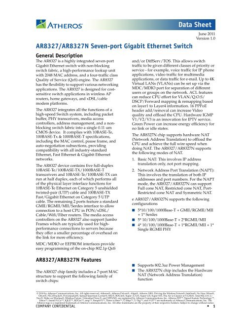
<strong>AR8327</strong> System Block Diagram<br />
n 40 MIBs Counter/Port & Port Status.<br />
n 1M Bit Packet Buffer<br />
n Sup<strong>port</strong>s 9K Jumbo Frame<br />
n Port Mirror, 802.1X Security, Rapid Spanning<br />
Tree<br />
n Rule-based Bandwidth Control<br />
n Programmable Wake on LAN<br />
n Half Power Mode for Cable length less than<br />
30m (for home installations)<br />
n Sup<strong>port</strong>s Internal/External Loopback<br />
n Sup<strong>port</strong>s Reduced AFE circuit<br />
n 2K MAC Table. Edit, Search, Add & Delete.<br />
n MAC Limit by Port/Chip/VLAN<br />
n Trunking Function<br />
n Sup<strong>port</strong>s Trunking and auto-failover<br />
n Power Saving on Cable no Link, short Cable<br />
& 10BASE-Te Idle<br />
n Sup<strong>port</strong>s 1K NAPT entries and 128<br />
hardware based host routing (ARP) entries<br />
n Sup<strong>port</strong>s hardware-based IP source guard,<br />
ARP inspection, routing/L3 switching<br />
n Sup<strong>port</strong>s VLAN translation and mapping<br />
with 64 Translation entries<br />
n 148 pin DRQFN, 0.11um<br />
Configuration<br />
Registers<br />
MB/Statistics<br />
Counters<br />
LED<br />
Controller<br />
7-Port <strong>Gigabit</strong> <strong>Ethernet</strong> <strong>Switch</strong> Engine<br />
QoS Engine Buffer Memory<br />
VLAN Table<br />
Lookup Engine MAC Table Memory<br />
MDC/MDIO<br />
Queue Manager<br />
Bandwidth Control<br />
EEPROM<br />
LED<br />
MDC/<br />
MDIO<br />
Port 0<br />
GMAC<br />
Port 1<br />
GMAC<br />
Port 2<br />
GMAC<br />
Port 3<br />
GMAC<br />
Port 4<br />
GMAC<br />
Port 5<br />
GMAC<br />
Port 6<br />
GMAC<br />
Port 0<br />
GMII/<br />
RGMII<br />
10/100 /1000<br />
Based -T<br />
PHY<br />
10/100 /1000<br />
Based -T<br />
PHY<br />
10/100 /1000<br />
Based -T<br />
PHY<br />
10/100 /1000<br />
Based -T<br />
PHY<br />
10/100 /1000<br />
Based -T<br />
PHY<br />
RGMII<br />
Serdes<br />
2 • <strong>AR8327</strong>/<strong>AR8327</strong>N <strong>Seven</strong>-<strong>port</strong> <strong>Gigabit</strong> <strong>Ethernet</strong> <strong>Switch</strong> Atheros Communications, Inc.<br />
2 • June 2011 COMPANY CONFIDENTIAL
Table of Contents<br />
General Description ........................................ 1<br />
<strong>AR8327</strong>/<strong>AR8327</strong>N Features .......................... 1<br />
<strong>AR8327</strong> System Block Diagram .................... 2<br />
Table of Contents ............................................ 3<br />
Revision History ........................................... 11<br />
1 Pin Descriptions .......................... 13<br />
2 Functional Description ............... 23<br />
2.1 Applications ............................................ 23<br />
2.1.1 AP Router Application .............. 23<br />
2.2 Atheros Header ...................................... 24<br />
2.2.1 Transmit ....................................... 25<br />
2.3 Receive ..................................................... 25<br />
2.4 Header for Read/Write Register. ........ 26<br />
2.5 Media Access Controllers (MAC) ........ 26<br />
2.6 Port Status Configuration ..................... 26<br />
2.6.1 Full-Duplex Flow Control ......... 26<br />
2.6.2 Half-Duplex Flow Control ........ 26<br />
2.6.3 Inter-Packet Gap (IPG) ............... 27<br />
2.6.4 Illegal Frames .............................. 27<br />
2.7 ACL .......................................................... 27<br />
2.7.1 ACL Rule ..................................... 27<br />
2.7.2 Action Definition ........................ 28<br />
2.7.3 MAC Pattern ............................... 29<br />
2.7.4 IPv4 Pattern ................................. 30<br />
2.7.5 IPv6 Pattern ................................. 32<br />
2.7.6 Window Pattern .......................... 34<br />
2.7.7 Enhanced MAC Pattern ............. 35<br />
2.7.8 Enhanced MAC Pattern ............. 35<br />
2.8 Register Access ....................................... 36<br />
2.9 LED Control ............................................ 37<br />
2.10 VLANs .................................................... 38<br />
2.10.1 Port-Based VLAN ....................... 38<br />
2.10.2 802.1Q VLANs ............................ 38<br />
2.10.3 VLAN Security ............................ 38<br />
2.10.4 Port Isolation ............................... 39<br />
2.10.5 Leaky VLAN ............................... 39<br />
2.10.6 VLAN Translation ...................... 39<br />
2.10.7 VLAN Translation Table ........... 39<br />
2.10.8 Egress Mode ................................ 40<br />
2.10.9 VLAN Table ................................. 41<br />
2.11 Security and Port Mapping ................. 41<br />
2.12 MIB/Statistics Counters ...................... 43<br />
2.13 Quality of Service (QoS) ...................... 45<br />
2.14 Mirroring ................................................ 45<br />
2.15 Rate Limiting ......................................... 46<br />
2.16 Broadcast Suppression ......................... 46<br />
2.17 IGMP/MLD Snooping ......................... 46<br />
2.17.1 IEEE 802.3 Reserved Group<br />
Addresses Filtering Control ...... 46<br />
2.17.2 802.1X ........................................... 46<br />
2.17.3 Forwarding Unknown ............... 47<br />
2.17.4 MAC Limit .................................. 47<br />
2.18 Spanning Tree ....................................... 47<br />
2.18.1 EEPROM Programming Format 47<br />
2.18.2 Basic <strong>Switch</strong> Operation .............. 47<br />
2.18.3 Lookup Engine ............................ 47<br />
2.18.4 Automatic Address Learning ... 48<br />
2.18.5 Automatic Address Aging ........ 48<br />
2.18.6 Broadcast/Multicast Storm Control<br />
48<br />
2.18.7 ARL Table .................................... 48<br />
2.19 HNAT ..................................................... 50<br />
2.19.1 Basic NAT Table ......................... 50<br />
2.19.2 NAPT Entry ................................. 51<br />
2.19.3 Router MAC Address ................ 52<br />
2.19.4 ARP ENTRY ................................ 53<br />
2.20 IEEE 802.3az and Energy Efficient<br />
<strong>Ethernet</strong> 53<br />
2.20.1 IEEE 802.3az LPI Mode .............. 54<br />
2.21 Memory Map ......................................... 55<br />
3 Register Descriptions ..................57<br />
3.1 Register Address Space (Address Range<br />
0x0000 ~ 0x00FC) 57<br />
3.2 Global Register Summary (Address Range<br />
0x0000 ~ 0x00B4) 58<br />
3.2.1 MASK_CTRL ............................... 59<br />
3.2.2 PORT0 PAD MODE CTRL ........ 59<br />
3.2.3 PORT5 PAD MODE CTRL ........ 60<br />
3.2.4 PORT6 PAD MODE CTRL ........ 61<br />
3.2.5 PWS_REG .................................... 63<br />
3.2.6 GLOBAL_INT0 ........................... 64<br />
3.2.7 GLOBAL_INT1 ........................... 65<br />
Atheros Communications, Inc.<br />
<strong>AR8327</strong>/<strong>AR8327</strong>N <strong>Seven</strong>-<strong>port</strong> <strong>Gigabit</strong> <strong>Ethernet</strong> <strong>Switch</strong> • 3<br />
COMPANY CONFIDENTIAL June 2011 • 3
3.2.8 GLOBAL_INT0 ........................... 66<br />
3.2.9 GLOBAL_INT1 ........................... 67<br />
3.2.10 MODULE_EN ............................. 68<br />
3.2.11 MIB ................................................ 68<br />
3.2.12 INTERFACE_HIGH_ADDR ..... 69<br />
3.2.13 MDIO Master Control ................ 70<br />
3.2.14 BIST_CTRL .................................. 70<br />
3.2.15 BIST_RECOVER .......................... 71<br />
3.2.16 SERVICE_TAG ............................ 72<br />
3.2.17 LED_CTRL0 ................................. 72<br />
3.2.18 LED_CTRL1 ................................. 72<br />
3.2.19 LED_CTRL2 ................................. 73<br />
3.2.20 LED_CTRL3 ................................. 73<br />
3.2.21 GOL_MAC_ADDR0 ................... 74<br />
3.2.22 GOL_MAC_ADDR1 ................... 74<br />
3.2.23 MAX_FRAME_SIZE ................... 74<br />
3.2.24 PORT0_STATUS ......................... 75<br />
3.2.25 PORT1_STATUS ......................... 76<br />
3.2.26 PORT2_STATUS ......................... 77<br />
3.2.27 PORT3_STATUS ......................... 78<br />
3.2.28 PORT4_STATUS ......................... 79<br />
3.2.29 PORT5_STATUS ......................... 80<br />
3.2.30 PORT6_STATUS ......................... 81<br />
3.2.31 HEADER_CTRL .......................... 82<br />
3.2.32 PORT0_HEADER_CTRL ........... 82<br />
3.2.33 PORT1_HEADER_CTRL ........... 83<br />
3.2.34 PORT2_HEADER_CTRL ........... 83<br />
3.2.35 PORT3_HEADER_CTRL ........... 84<br />
3.2.36 PORT4_HEADER_CTRL ........... 85<br />
3.2.37 PORT5_HEADER_CTRL ........... 85<br />
3.2.38 PORT6_HEADER_CTRL ........... 86<br />
3.2.39 SGMII Control Register ............. 86<br />
3.3 EEE CTRL REGISTER SUMMARY<br />
(Address Range 0x0100 ~ 0x0168) 89<br />
3.3.1 EEE_CTRL ................................... 89<br />
3.3.2 EEE_LOC_VALUE_1 ................. 90<br />
3.3.3 EEE_REM_VALUE_1 ................. 90<br />
3.3.4 EEE_RES_VALUE_1 ................... 90<br />
3.3.5 EEE_LOC_VALUE_2 ................. 90<br />
3.3.6 EEE_REM_VALUE_2 ................. 91<br />
3.3.7 EEE_RES_VALUE_2 ................... 91<br />
3.3.8 EEE_LOC_VALUE_3 ................. 91<br />
3.3.9 EEE_REM_VALUE_3 ................. 92<br />
3.3.10 EEE_RES_VALUE_3 ................... 92<br />
3.3.11 EEE_LOC_VALUE_4 ................. 92<br />
3.3.12 EEE_REM_VALUE_4 ................. 93<br />
3.3.13 EEE_RES_VALUE_4 .................. 93<br />
3.3.14 EEE_LOC_VALUE_5 ................. 93<br />
3.3.15 EEE_REM_VALUE_5 ................. 94<br />
3.3.16 EEE_RES_VALUE_5 .................. 94<br />
3.4 PARSER REGISTER SUMMARY(Address<br />
Range 0x0200 ~ 0x0270) 95<br />
3.4.1 NORMALIZE_CTRL0 ................ 95<br />
3.4.2 NORMALIZE_CTRL1 ................ 97<br />
3.4.3 NORMALIZE_LEN_CTRL ....... 98<br />
3.4.4 FRAM_ACK_CTRL0 .................. 98<br />
3.4.5 FRAM_ACK_CTRL1 ................ 100<br />
3.4.6 WIN_RULE_CTRL0 ................. 101<br />
3.4.7 WIN_RULE_CTRL1 ................. 101<br />
3.4.8 WIN_RULE_CTRL2 ................. 102<br />
3.4.9 WIN_RULE_CTRL3 ................. 103<br />
3.4.10 WIN_RULE_CTRL4 ................. 103<br />
3.4.11 WIN_RULE_CTRL5 ................. 104<br />
3.4.12 WIN_RULE_CTRL6 ................. 104<br />
3.4.13 WIN_RULE_CTRL7 ................. 105<br />
3.4.14 WIN_RULE_CTRL8 ................. 105<br />
3.4.15 WIN_RULE_CTRL9 ................. 106<br />
3.4.16 WIN_RULE_CTRL10 ............... 106<br />
3.4.17 WIN_RULE_CTRL11 ............... 107<br />
3.4.18 WIN_RULE_CTRL12 ............... 107<br />
3.4.19 WIN_RULE_CTRL13 ............... 108<br />
3.4.20 TRUNK_HASH_EN ................. 108<br />
3.5 ACL REGISTER (Address Range: 0x0400 ~<br />
0x0454) 109<br />
3.5.1 ACL_FUNC0 ............................. 109<br />
3.5.2 ACL_FUNC1 ............................. 109<br />
3.5.3 ACL_FUNC2 ............................. 110<br />
3.5.4 ACL_FUNC3 ............................. 110<br />
3.5.5 ACL_FUNC4 ............................. 110<br />
3.5.6 ACL_FUNC5 ............................. 111<br />
3.5.7 PRIVATE_IP_CTRL ................. 111<br />
3.5.8 PORT0_VLAN_CTRL0 ............ 111<br />
3.5.9 PORT0_VLAN_CTRL1 ............ 112<br />
3.5.10 PORT1_VLAN_CTRL0 ............ 113<br />
3.5.11 PORT1_VLAN_CTRL1 ............ 114<br />
3.5.12 PORT2_VLAN_CTRL0 ............ 115<br />
3.5.13 PORT2_VLAN_CTRL1 ............ 116<br />
3.5.14 PORT3_VLAN_CTRL0 ............ 116<br />
3.5.15 PORT3_VLAN_CTRL1 ............ 117<br />
3.5.16 PORT4_VLAN_CTRL0 ............ 118<br />
4 • <strong>AR8327</strong>/<strong>AR8327</strong>N <strong>Seven</strong>-<strong>port</strong> <strong>Gigabit</strong> <strong>Ethernet</strong> <strong>Switch</strong> Atheros Communications, Inc.<br />
4 • June 2011 COMPANY CONFIDENTIAL
3.5.17 PORT4_VLAN_CTRL1 ............ 119<br />
3.5.18 PORT5_VLAN_CTRL0 ............ 119<br />
3.5.19 PORT5_VLAN_CTRL1 ............ 120<br />
3.5.20 PORT6_VLAN_CTRL0 ............ 121<br />
3.5.21 PORT6_VLAN_CTRL1 ............ 122<br />
3.5.22 IPv6 Private Base Address Register<br />
0 ................................................... 122<br />
3.5.23 IPv6 Private Base Address Register<br />
1 ................................................... 123<br />
3.5.24 IPv6 Private Base Address Register<br />
2 ................................................... 123<br />
3.6 LOOKUP REGISTER (Address Range:<br />
0x0600 ~ 0x0708) 124<br />
3.6.1 ATU_DATA0 ............................. 125<br />
3.6.2 ATU_DATA1 ............................. 125<br />
3.6.3 ATU_DATA2 ............................. 126<br />
3.6.4 ATU_FUNC_REG ..................... 126<br />
3.6.5 VTU_FUNC_REG0 ................... 128<br />
3.6.6 VTU_FUNC_REG1 ................... 129<br />
3.6.7 ARL_CTRL ................................ 130<br />
3.6.8 GLOBAL_FW_CTRL0 .............. 131<br />
3.6.9 GLOBAL_FW_CTRL1 .............. 133<br />
3.6.10 GOL_LEARN_LIMIT ............... 133<br />
3.6.11 TOS_PRI_MAP_REG0 ............. 134<br />
3.6.12 TOS_PRI_MAP_REG1 ............. 135<br />
3.6.13 TOS_PRI_MAP_REG2 ............. 135<br />
3.6.14 TOS_PRI_MAP_REG3 ............. 136<br />
3.6.15 TOS_PRI_MAP_REG4 ............. 136<br />
3.6.16 TOS_PRI_MAP_REG5 ............. 137<br />
3.6.17 TOS_PRI_MAP_REG6 ............. 137<br />
3.6.18 TOS_PRI_MAP_REG7 ............. 138<br />
3.6.19 VLAN_PRI_MAP_REG0 ......... 138<br />
3.6.20 LOOP_CHECK_RESULT ........ 139<br />
3.6.21 PORT0_LOOKUP_CTRL ......... 139<br />
3.6.22 PORT0_PRI_CTRL .................... 142<br />
3.6.23 PORT0_LEARN_LIMIT ........... 143<br />
3.6.24 PORT1_LOOKUP_CTRL ......... 144<br />
3.6.25 PORT1_PRI_CTRL Address 0x0670<br />
147<br />
3.6.26 PORT1_LEARN_LIMIT ........... 148<br />
3.6.27 PORT2_LOOKUP_CTRL ......... 149<br />
3.6.28 PORT2_PRI_CTRL .................... 151<br />
3.6.29 PORT2_LEARN_LIMIT ........... 152<br />
3.6.30 PORT3_LOOKUP_CTRL ......... 153<br />
3.6.31 PORT3_PRI_CTRL .................... 156<br />
3.6.32 PORT3_LEARN_LIMIT ........... 157<br />
3.6.33 PORT4_LOOKUP_CTRL ......... 158<br />
3.6.34 PORT4_PRI_CTRL ................... 160<br />
3.6.35 PORT4_LEARN_LIMIT ........... 161<br />
3.6.36 PORT5_LOOKUP_CTRL ......... 162<br />
3.6.37 PORT5_PRI_CTRL ................... 165<br />
3.6.38 PORT5_LEARN_LIMIT ........... 166<br />
3.6.39 PORT6_LOOKUP_CTRL ......... 167<br />
3.6.40 PORT6_PRI_CTRL ................... 170<br />
3.6.41 PORT6_LEARN_LIMIT ........... 171<br />
3.6.42 GOL_TRUNK_CTRL0 ............. 172<br />
3.6.43 GOL_TRUNK_CTRL1 ............. 173<br />
3.6.44 GOL_TRUNK_CTRL2 ............. 174<br />
3.7 QM REGISTER(BASE ADDR:0x0800) 175<br />
3.7.1 GLOBAL_FLOW_THD ........... 180<br />
3.7.2 QM_CTRL_REG ....................... 180<br />
3.7.3 WAN_QUEUE_MAP_REG ..... 182<br />
3.7.4 LAN_QUEUE_MAP_REG ...... 183<br />
3.7.5 PORT0_WRR_CTRL ................ 184<br />
3.7.6 PORT1_WRR_CTRL ................ 185<br />
3.7.7 PORT2_WRR_CTRL ................ 185<br />
3.7.8 PORT3_WRR_CTRL ................ 186<br />
3.7.9 PORT4_WRR_CTRL ................ 187<br />
3.7.10 PORT5_WRR_CTRL ................ 188<br />
3.7.11 PORT6_WRR_CTRL ................ 189<br />
3.7.12 PORT0_EG_RATE_CTRL0 ...... 190<br />
3.7.13 PORT0_EG_RATE_CTRL1 ...... 191<br />
3.7.14 PORT0_EG_RATE_CTRL2 ...... 192<br />
3.7.15 PORT0_EG_RATE_CTRL3 ...... 192<br />
3.7.16 PORT0_EG_RATE_CTRL4 ...... 193<br />
3.7.17 PORT0_EG_RATE_CTRL5 ...... 194<br />
3.7.18 PORT0_EG_RATE_CTRL6 ...... 194<br />
3.7.19 PORT0_EG_RATE_CTRL7 ...... 198<br />
3.7.20 PORT1_EG_RATE_CTRL0 ...... 202<br />
3.7.21 PORT1_EG_RATE_CTRL0 ...... 203<br />
3.7.22 PORT1_EG_RATE_CTRL3 ...... 203<br />
3.7.23 PORT1_EG_RATE_CTRL0 ...... 204<br />
3.7.24 PORT1_EG_RATE_CTRL6 ...... 205<br />
3.7.25 PORT1_EG_RATE_CTRL7 ...... 206<br />
3.7.26 PORT2_EG_RATE_CTRL0 ...... 207<br />
3.7.27 PORT2_EG_RATE_CTRL0 ...... 208<br />
3.7.28 PORT2_EG_RATE_CTRL0 ...... 208<br />
3.7.29 PORT2_EG_RATE_CTRL0 ...... 209<br />
3.7.30 PORT2_EG_RATE_CTRL0 ...... 210<br />
Atheros Communications, Inc.<br />
<strong>AR8327</strong>/<strong>AR8327</strong>N <strong>Seven</strong>-<strong>port</strong> <strong>Gigabit</strong> <strong>Ethernet</strong> <strong>Switch</strong> • 5<br />
COMPANY CONFIDENTIAL June 2011 • 5
3.7.31 PORT2_EG_RATE_CTRL0 ...... 211<br />
3.7.32 PORT3_EG_RATE_CTRL0 ...... 212<br />
3.7.33 PORT3_EG_RATE_CTRL0 ...... 213<br />
3.7.34 PORT3_EG_RATE_CTRL2 ...... 213<br />
3.7.35 PORT3_EG_RATE_CTRL2 ...... 214<br />
3.7.36 PORT3_EG_RATE_CTRL5 ...... 215<br />
3.7.37 PORT3_EG_RATE_CTRL5 ...... 216<br />
3.7.38 PORT4_EG_RATE_CTRL5 ...... 217<br />
3.7.39 PORT4_EG_RATE_CTRL5 ...... 218<br />
3.7.40 PORT4_EG_RATE_CTRL5 ...... 218<br />
3.7.41 PORT4_EG_RATE_CTRL5 ...... 219<br />
3.7.42 PORT4_EG_RATE_CTRL6 ...... 220<br />
3.7.43 PORT4_EG_RATE_CTRL7 ...... 221<br />
3.7.44 PORT5_EG_RATE_CTRL0 ...... 222<br />
3.7.45 PORT5_EG_RATE_CTRL1 ...... 223<br />
3.7.46 PORT5_EG_RATE_CTRL2 ...... 223<br />
3.7.47 PORT5_EG_RATE_CTRL3 ...... 224<br />
3.7.48 PORT5_EG_RATE_CTRL4 ...... 225<br />
3.7.49 PORT5_EG_RATE_CTRL5 ...... 225<br />
3.7.50 PORT5_EG_RATE_CTRL6 ...... 226<br />
3.7.51 PORT5_EG_RATE_CTRL7 ...... 227<br />
3.7.52 PORT6_EG_RATE_CTRL0 ...... 229<br />
3.7.53 PORT6_EG_RATE_CTRL1 ...... 230<br />
3.7.54 PORT6_EG_RATE_CTRL2 ...... 230<br />
3.7.55 PORT6_EG_RATE_CTRL3 ...... 231<br />
3.7.56 PORT6_EG_RATE_CTRL4 ...... 232<br />
3.7.57 PORT6_EG_RATE_CTRL5 ...... 232<br />
3.7.58 PORT6_EG_RATE_CTRL6 ...... 233<br />
3.7.59 PORT6_EG_RATE_CTRL6 ...... 234<br />
3.7.60 PORT0_HOL_CTRL0 ............... 236<br />
3.7.61 PORT0_HOL_CTRL1 ............... 237<br />
3.7.62 PORT1_HOL_CTRL0 ............... 238<br />
3.7.63 PORT1_HOL_CTRL1 ............... 239<br />
3.7.64 PORT2_HOL_CTRL0 ............... 240<br />
3.7.65 PORT2_HOL_CTRL1 ............... 241<br />
3.7.66 PORT3_HOL_CTRL0 ............... 242<br />
3.7.67 PORT3_HOL_CTRL1 ............... 243<br />
3.7.68 PORT4_HOL_CTRL0 ............... 244<br />
3.7.69 PORT4_HOL_CTRL1 ............... 245<br />
3.7.70 PORT5_HOL_CTRL0 ............... 246<br />
3.7.71 PORT5_HOL_CTRL1 ............... 247<br />
3.7.72 PORT6_HOL_CTRL0 ............... 248<br />
3.7.73 PORT6_HOL_CTRL1 ............... 249<br />
3.7.74 PORT0_FLOW_THD ................ 250<br />
3.7.75 PORT1_FLOW_THD ................ 250<br />
3.7.76 PORT2_FLOW_THD ............... 251<br />
3.7.77 PORT3_FLOW_THD ............... 252<br />
3.7.78 PORT4_FLOW_THD ............... 252<br />
3.7.79 PORT5_FLOW_THD ............... 253<br />
3.7.80 PORT6_FLOW_THD ............... 253<br />
3.7.81 ACL_POLICY_MODE ............. 254<br />
3.7.82 ACL_COUNTER_MODE ........ 256<br />
3.7.83 ACL_CNT_RESET .................... 258<br />
3.7.84 ACL_RATE_CTRL0 ................. 259<br />
3.7.85 ACL_RATE_CTRL1_0 ............. 260<br />
3.7.86 ACL_RATE_CTRL0_1 ............. 261<br />
3.7.87 ACL_RATE_CTRL1_1 ............. 261<br />
3.7.88 ACL_RATE_CTRL0_2 ............. 262<br />
3.7.89 ACL_RATE_CTRL1_2 ............. 263<br />
3.7.90 ACL_RATE_CTRL0_3 ............. 264<br />
3.7.91 ACL_RATE_CTRL1_3 ............. 264<br />
3.7.92 ACL_RATE_CTRL0_4 ............. 265<br />
3.7.93 ACL_RATE_CTRL1_4 ............. 266<br />
3.7.94 ACL_RATE_CTRL1_5 ............. 267<br />
3.7.95 ACL_RATE_CTRL1_5 ............. 267<br />
3.7.96 ACL_RATE_CTRL0_6 ............. 268<br />
3.7.97 ACL_RATE_CTRL1_6 ............. 268<br />
3.7.98 ACL_RATE_CTRL1_7 ............. 269<br />
3.7.99 ACL_RATE_CTRL1_7 ............. 270<br />
3.7.100 ACL_RATE_CTRL0_8 ............ 270<br />
3.7.101 ACL_RATE_CTRL1_8 ............ 271<br />
3.7.102 ACL_RATE_CTRL0_9 ............ 272<br />
3.7.103 ACL_RATE_CTRL1_9 ............ 272<br />
3.7.104 ACL_RATE_CTRL0_10 .......... 273<br />
3.7.105 ACL_RATE_CTRL0_10 .......... 274<br />
3.7.106 ACL_RATE_CTRL0_11 .......... 274<br />
3.7.107 ACL_RATE_CTRL1_11 .......... 275<br />
3.7.108 ACL_RATE_CTRL0_12 .......... 276<br />
3.7.109 ACL_RATE_CTRL1_12 .......... 276<br />
3.7.110 ACL_RATE_CTRL0_13 .......... 277<br />
3.7.111 ACL_RATE_CTRL1_13 .......... 277<br />
3.7.112 ACL_RATE_CTRL0_14 .......... 278<br />
3.7.113 ACL_RATE_CTRL1_14 .......... 278<br />
3.7.114 ACL_RATE_CTRL0_15 .......... 279<br />
3.7.115 ACL_RATE_CTRL1_15 .......... 280<br />
3.7.116 ACL_RATE_CTRL1_16 .......... 280<br />
3.7.117 ACL_RATE_CTRL1_16 .......... 281<br />
3.7.118 ACL_RATE_CTRL1_17 .......... 282<br />
3.7.119 ACL_RATE_CTRL1_17 .......... 282<br />
3.7.120 ACL_RATE_CTRL0_18 .......... 283<br />
6 • <strong>AR8327</strong>/<strong>AR8327</strong>N <strong>Seven</strong>-<strong>port</strong> <strong>Gigabit</strong> <strong>Ethernet</strong> <strong>Switch</strong> Atheros Communications, Inc.<br />
6 • June 2011 COMPANY CONFIDENTIAL
3.7.121 ACL_RATE_CTRL0_18 .......... 284<br />
3.7.122 ACL_RATE_CTRL0_19 .......... 284<br />
3.7.123 ACL_RATE_CTRL1_19 .......... 285<br />
3.7.124 ACL_RATE_CTRL1_20 .......... 286<br />
3.7.125 ACL_RATE_CTRL1_20 .......... 286<br />
3.7.126 ACL_RATE_CTRL0_21 .......... 287<br />
3.7.127 ACL_RATE_CTRL1_21 .......... 287<br />
3.7.128 ACL_RATE_CTRL0_22 .......... 288<br />
3.7.129 ACL_RATE_CTRL1_22 .......... 289<br />
3.7.130 ACL_RATE_CTRL0_23 .......... 289<br />
3.7.131 ACL_RATE_CTRL1_23 .......... 290<br />
3.7.132 ACL_RATE_CTRL0_24 .......... 291<br />
3.7.133 ACL_RATE_CTRL1_24 .......... 291<br />
3.7.134 ACL_RATE_CTRL0_25 .......... 292<br />
3.7.135 ACL_RATE_CTRL1_25 .......... 292<br />
3.7.136 ACL_RATE_CTRL0_26 .......... 293<br />
3.7.137 ACL_RATE_CTRL1_26 .......... 293<br />
3.7.138 ACL_RATE_CTRL0_27 .......... 294<br />
3.7.139 ACL_RATE_CTRL1_27 .......... 295<br />
3.7.140 ACL_RATE_CTRL0_28 .......... 295<br />
3.7.141 ACL_RATE_CTRL1_28 .......... 296<br />
3.7.142 ACL_RATE_CTRL0_29 .......... 297<br />
3.7.143 ACL_RATE_CTRL1_29 .......... 297<br />
3.7.144 ACL_RATE_CTRL0_30 .......... 298<br />
3.7.145 ACL_RATE_CTRL1_30 .......... 298<br />
3.7.146 ACL_RATE_CTRL0_31 .......... 299<br />
3.7.147 ACL_RATE_CTRL1_31 .......... 300<br />
3.7.148 PORT0_ING_RATE_CTRL0 .. 301<br />
3.7.149 PORT0_ING_RATE_CTRL1 .. 302<br />
3.7.150 PORT0_ING_RATE_CTRL2 .. 302<br />
3.7.151 PORT1_ING_RATE_CTRL0 .. 303<br />
3.7.152 PORT1_ING_RATE_CTRL1 .. 304<br />
3.7.153 PORT1_ING_RATE_CTRL2 .. 305<br />
3.7.154 PORT2_ING_RATE_CTRL0 .. 306<br />
3.7.155 PORT2_ING_RATE_CTRL0 .. 307<br />
3.7.156 PORT2_ING_RATE_CTRL2 .. 308<br />
3.7.157 PORT3_ING_RATE_CTRL0 .. 308<br />
3.7.158 PORT3_ING_RATE_CTRL0 .. 309<br />
3.7.159 PORT3_ING_RATE_CTRL2 .. 310<br />
3.7.160 PORT4_ING_RATE_CTRL0 .. 311<br />
3.7.161 PORT4_ING_RATE_CTRL0 .. 312<br />
3.7.162 PORT4_ING_RATE_CTRL2 .. 313<br />
3.7.163 PORT5 _ING_RATE_CTRL0 . 314<br />
3.7.164 PORT5_ING_RATE_CTRL1 .. 315<br />
3.7.165 PORT5_ING_RATE_CTRL2 .. 315<br />
3.7.166 PORT6 _ING_RATE_CTRL0 . 316<br />
3.7.167 PORT6_ING_RATE_CTRL1 .. 317<br />
3.7.168 PORT6_ING_RATE_CTRL2 .. 318<br />
3.7.169 CPU_GROUP_CTRL .............. 319<br />
3.8 PKT EDIT REGISTER(Address Range<br />
0x0C00 ~ 0x0C64) 321<br />
3.8.1 PKT_EDIT_CTRL ..................... 321<br />
3.8.2 PORT0_QUEUE_REMAP_REG1 .<br />
322<br />
3.8.3 PORT1_QUEUE_REMAP_REG0 .<br />
323<br />
3.8.4 PORT2_QUEUE_REMAP_REG0 .<br />
323<br />
3.8.5 PORT3_QUEUE_REMAP_REG0 .<br />
324<br />
3.8.6 PORT4_QUEUE_REMAP_REG0 .<br />
325<br />
3.8.7 PORT5_QUEUE_REMAP_REG0 .<br />
325<br />
3.8.8 PORT5_QUEUE_REMAP_REG1 .<br />
326<br />
3.8.9 PORT6_QUEUE_REMAP_REG0 .<br />
326<br />
3.8.10 PORT6_QUEUE_REMAP_REG0 .<br />
327<br />
3.8.11 Router Default VID Register 0 328<br />
3.8.12 Router Default VID Register 1 328<br />
3.8.13 Router Default VID Register 2 328<br />
3.8.14 Router Default VID Register 3 329<br />
3.8.15 Router Egress VLAN Mode .... 329<br />
3.9 L3 REGISTER (Address Range 0x0E00 ~<br />
0x0E5C) 330<br />
3.9.1 HRouter_control ....................... 330<br />
3.9.2 HRouter_Pbased_Control0 ..... 331<br />
3.9.3 HRouter_Pbased_Control1 ..... 331<br />
3.9.4 HRouter_Pbased_Control2 ..... 332<br />
3.9.5 WCMP_HASH_TABLE0 ......... 333<br />
3.9.6 WCMP_HASH_TABLE1 ......... 333<br />
3.9.7 WCMP_HASH_TABLE2 ......... 333<br />
3.9.8 WCMP_HASH_TABLE3 ......... 334<br />
3.9.9 WCMP_NHOP_TABLE0 ......... 334<br />
3.9.10 WCMP_NHOP_TABLE1 ......... 334<br />
3.9.11 WCMP_NHOP_TABLE2 ......... 335<br />
3.9.12 WCMP_NHOP_TABLE3 ......... 335<br />
3.9.13 ARP_Entry_Lock_Control ....... 336<br />
3.9.14 ARP_Used_Account ................. 336<br />
Atheros Communications, Inc.<br />
<strong>AR8327</strong>/<strong>AR8327</strong>N <strong>Seven</strong>-<strong>port</strong> <strong>Gigabit</strong> <strong>Ethernet</strong> <strong>Switch</strong> • 7<br />
COMPANY CONFIDENTIAL June 2011 • 7
3.9.15 HNAT_Control ......................... 336<br />
3.9.16 NAPT_Entry_Lock_Control0 .. 338<br />
3.9.17 NAPT_Entry_Lock_Control1 .. 338<br />
3.9.18 NAPT_Used_Account .............. 339<br />
3.9.19 Entry_Edit_Data0 ..................... 339<br />
3.9.20 Entry_Edit_Data1 ..................... 339<br />
3.9.21 Entry_Edit_Data2 ..................... 339<br />
3.9.22 Entry_Edit_Data3 ..................... 340<br />
3.9.23 Entry_Edit_control ................... 340<br />
3.9.24 Private_Base_IP_ADDR Register .<br />
341<br />
3.10 PHY Control Registers ....................... 343<br />
3.10.1 Control Register ........................ 344<br />
3.10.2 Status Register ........................... 346<br />
3.10.3 PHY Identifier ........................... 347<br />
3.10.4 PHY Identifier 2 ........................ 348<br />
3.10.5 Auto-negotiation Advertisement<br />
Register ....................................... 348<br />
3.10.6 Link Partner Ability Register .. 350<br />
3.10.7 Auto-negotiation Expansion<br />
Register ....................................... 352<br />
3.10.8 Next Page Transmit Register .. 352<br />
3.10.9 Link Partner Next Page Register ..<br />
353<br />
3.10.10 1000Base-T Control Register . 354<br />
3.10.11 1000Base-T Status Register .... 355<br />
3.10.12 MMD Access Control Register 356<br />
3.10.13 MMD Access Address Data<br />
Register ....................................... 357<br />
3.10.14 Extended Status Register ....... 357<br />
3.10.15 Function Control Register ...... 358<br />
3.10.16 PHY Specific Status Register . 359<br />
3.10.17 Interrupt Enable Register ....... 360<br />
3.10.18 Interrupt Status Register ........ 362<br />
3.10.19 Smart Speed Register .............. 363<br />
3.10.20 Receive Error Counter Register ..<br />
364<br />
3.10.21 Virtual Cable Tester Control<br />
Register ....................................... 365<br />
3.10.22 Virtual Cable Tester Status<br />
Register ....................................... 365<br />
3.10.23 Debug Port ............................... 366<br />
3.10.24 Debug Port 2 (R/W Port) ....... 366<br />
3.10.25 Debug Register — Analog Test<br />
Control ........................................ 367<br />
3.10.26 Debug Register — System Mode<br />
Control ....................................... 368<br />
3.10.27 Debug Register — System Mode<br />
Control ....................................... 369<br />
3.10.28 Debug Register—Hib Control and<br />
Auto Negotiation Test Register 371<br />
3.10.29 Debug Register — RGMII Mode<br />
Selection ..................................... 372<br />
3.10.30 Debug Register—Green Feature<br />
Configure Register ................... 373<br />
3.11 MMD3 — PCS Register ...................... 374<br />
3.11.1 PCS Control1 ............................. 374<br />
3.11.2 PCS Status1 ................................ 374<br />
3.12 EEE Capability Register ..................... 376<br />
3.12.1 EEE Wake Error Counter ........ 376<br />
3.13 MMD7 — Auto-negotiation Register 377<br />
3.13.1 AN Package ............................... 377<br />
3.13.2 AN Status ................................... 378<br />
3.13.3 AN XNP Transmit .................... 378<br />
3.13.4 AN XNP Transmit1 .................. 379<br />
3.13.5 AN XNP Transmit2 .................. 379<br />
3.13.6 AN LP XNP Ability .................. 379<br />
3.13.7 AN LP XNP Ability1 ................ 380<br />
3.13.8 AN LP XNP Ability2 ................ 380<br />
3.13.9 EEE Advertisement .................. 380<br />
3.13.10 EEE LP Advertisement .......... 381<br />
3.13.11 EEE Ability Auto-negotiation<br />
Result .......................................... 382<br />
4 Electrical Characteristics ..........383<br />
4.1 Absolute Maximum Ratings .............. 383<br />
4.2 Recommended Operating Conditions 383<br />
4.3 RGMII/GMII Characteristics ............. 383<br />
4.4 Power-on Strapping ............................ 384<br />
4.4.12 Power-on-Reset Timing ........... 385<br />
4.5 AC Timing ............................................ 385<br />
4.5.1 XTAL/OSC Timing .................. 385<br />
4.5.2 MII Timing ................................. 386<br />
4.5.3 GMII Timing ............................. 387<br />
4.5.4 RGMII Timing ........................... 388<br />
4.5.5 SPI Timing ................................. 389<br />
4.5.6 MDIO Timing ............................ 389<br />
4.6 Typical Power Consumption Parameters<br />
390<br />
5 Package Dimensions .................391<br />
8 • <strong>AR8327</strong>/<strong>AR8327</strong>N <strong>Seven</strong>-<strong>port</strong> <strong>Gigabit</strong> <strong>Ethernet</strong> <strong>Switch</strong> Atheros Communications, Inc.<br />
8 • June 2011 COMPANY CONFIDENTIAL
6 Ordering Information ............... 393<br />
7 Top Side Marking ..................... 393<br />
Atheros Communications, Inc.<br />
<strong>AR8327</strong>/<strong>AR8327</strong>N <strong>Seven</strong>-<strong>port</strong> <strong>Gigabit</strong> <strong>Ethernet</strong> <strong>Switch</strong> • 9<br />
COMPANY CONFIDENTIAL June 2011 • 9
10 • <strong>AR8327</strong>/<strong>AR8327</strong>N <strong>Seven</strong>-<strong>port</strong> <strong>Gigabit</strong> <strong>Ethernet</strong> <strong>Switch</strong> Atheros Communications, Inc.<br />
10 • June 2011 COMPANY CONFIDENTIAL
Revision History<br />
Table 0-1. AR8161-A Revision History<br />
Date Revision Details Revision<br />
2011/2/24 First draft 0.31<br />
2011/6/10 General<br />
n Typo and grammar corrections<br />
n Reference corrections<br />
Pin Description<br />
n Update drawing to re-organize inner(B) and outer (A) pins<br />
n Table 1-1: change A54 pin type to I/O, PU<br />
Function Descriptions<br />
n Table 2-34 and 2-35: change PRIVATE_IP_ADDR_MODE to<br />
PRIVATE_IP_BASE_SEL<br />
n 2.7.2 Action Definition: add description<br />
n 2.21 Memory Map: update memory map<br />
Registers<br />
n 3.2.2 PORT0 PAD MODE CTRL, update bit[18] bit[19] definitions<br />
n 3.2.3 PORT5 PAD MODE CTRL (0x0008): add description for bit[10]<br />
n 3.2.5 PWS_REG (0x0010): update bit definitions<br />
n 3.5.22 to 3.5.24 IPv6 Private Base Address Register 0-2: new registers<br />
n 3.8.12 to 3.8.14 Router Default VID Register 0-2: new registers<br />
n 3.8.16 Router Egress VLAN Mode (0x0C80): new register<br />
n 3.10.24 Debug Port 2 (0xIE): change decimal address to “0d30“<br />
n 3.10.25 Debug Register—Analog Test Control (0x00): new register<br />
n 3.10.26 Debug Register—System Mode Control (0x03): new register<br />
n 3.10.28 Debug Register—Hib Control and Auto Negotiation Test Register<br />
(0x0B): new register<br />
n 3.10.30 Debug Register—Green Feature Configure Register (0x3D): new<br />
register<br />
n 3.13 MMD7—Auto-negotiation Register: update bit definitions<br />
n 3.13.3 to 3.13.7: update decimal address<br />
n 4.6 Typical Power Consumption Parameters: update “two <strong>port</strong>s active” and<br />
“three <strong>port</strong>s active“ values<br />
Package Dimensions<br />
n Update package illustration<br />
Ordering<br />
n Update ordering method for tape&reel and tray<br />
Top Side Marking<br />
n Add package top marking illustration<br />
1<br />
Atheros Communications, Inc.<br />
<strong>Switch</strong> • 11<br />
<strong>AR8327</strong>/<strong>AR8327</strong>N <strong>Seven</strong>-<strong>port</strong> <strong>Gigabit</strong> <strong>Ethernet</strong>
12 • <strong>AR8327</strong>/<strong>AR8327</strong>N <strong>Seven</strong>-<strong>port</strong> <strong>Gigabit</strong> <strong>Ethernet</strong> <strong>Switch</strong> Atheros Communications, Inc.<br />
12 • June 2011 COMPANY CONFIDENTIAL
1. Pin Descriptions<br />
This section contains a listing of the signal<br />
descriptions (see Table 1-1 and Figure 1-1<br />
through Figure 1-2).<br />
The following nomenclature is used for signal<br />
names:<br />
_L<br />
N<br />
NC<br />
P<br />
At the end of the signal name,<br />
indicates active low signals<br />
At the end of the signal name<br />
indicates the negative side of a<br />
differential signal<br />
No connection should be made to<br />
this pin<br />
At the end of the signal name,<br />
indicates the positive side of a<br />
differential signal<br />
The following nomenclature is used for signal<br />
types described in Table 1-1:<br />
D<br />
I<br />
I/O<br />
IA<br />
IH<br />
IL<br />
O<br />
OA<br />
Open drain for digital pads<br />
Digital input signal<br />
Digital bidirectional signal<br />
Analog input signal<br />
Digital input with hysteresis<br />
Input signals with weak internal<br />
pull-down, to prevent signals<br />
from floating when left open<br />
Digital output signal<br />
Analog output signal<br />
P<br />
PD<br />
PU<br />
A power or ground signal<br />
Internal pull-down for digital<br />
input<br />
Internal pull-up for digital input<br />
Atheros Communications, Inc.<br />
<strong>Switch</strong> • 13<br />
<strong>AR8327</strong>/<strong>AR8327</strong>N <strong>Seven</strong>-<strong>port</strong> <strong>Gigabit</strong> <strong>Ethernet</strong>
B76<br />
B75<br />
A86<br />
A85<br />
A84<br />
B74<br />
B73<br />
B72<br />
B71<br />
B70<br />
A83<br />
A82<br />
A81<br />
A80<br />
A79<br />
B69<br />
A78<br />
B68<br />
B67<br />
B66<br />
A77<br />
A76<br />
A75<br />
B65<br />
A74<br />
B64<br />
B63<br />
A73<br />
B62<br />
A72<br />
A71<br />
B61<br />
B60<br />
A70<br />
A69<br />
B59<br />
A68<br />
DVDD<br />
VDD33_SVR<br />
LX<br />
LED_LINK1000n_3<br />
LED_LINK100n_3<br />
LED_LINK10n_3<br />
VDD25_IO<br />
LED_LINK1000n_2<br />
LED_LINK100n_2<br />
LED_LINK10n_2<br />
LED_LINK1000n_1<br />
LED_LINK100n_1<br />
LED_LINK10n_1<br />
LED_LINK1000n_0<br />
LED_LINK100n_0<br />
LED_LINK10n_0<br />
INTN<br />
SIP<br />
SIN<br />
AVDD<br />
SOP<br />
SON<br />
TESTMODE<br />
TXD3_0<br />
TXD2_0<br />
TXD1_0<br />
TXD0_0<br />
GTXCLK_0/TXCLK_0<br />
FILCAP1_15_0<br />
TXEN/TXCTR_0<br />
DVDD<br />
FILCAP0_15_0<br />
RXD3_0<br />
RXD2_0<br />
VDD15_REG_0<br />
RXD1_0<br />
RXD0_0<br />
DVDD<br />
FILCAP0<br />
CH0_TRXP0<br />
CH0_TRXN0<br />
AVDD<br />
CH0_TRXP1<br />
CH0_TRXN1<br />
VDD33<br />
CH0_TRXP2<br />
CH0_TRXN2<br />
AVDD<br />
CH0_TRXP3<br />
CH0_TRXN3<br />
VDD25_REG<br />
VREF<br />
VDD33<br />
RBIAS0<br />
AVDD25<br />
XTLI<br />
AVDDCO_0<br />
XTLO<br />
AVDD<br />
FILCAP2<br />
CH1_TRXP0<br />
CH1_TRXN0<br />
AVDD<br />
CH1_TRXP1<br />
CH1_TRXN1<br />
VDD33<br />
CH1_TRXP2<br />
CH1_TRXN2<br />
AVDD<br />
CH1_TRXP3<br />
CH1_TRXN3<br />
FILCAP3<br />
DVDD<br />
FILCAP4<br />
B1<br />
A3<br />
B2<br />
A4<br />
B3<br />
A5<br />
B4<br />
A6<br />
B5<br />
A7<br />
B6<br />
A8<br />
B7<br />
A9<br />
B8<br />
A10<br />
B9<br />
A11<br />
B10<br />
A12<br />
B11<br />
A13<br />
B12<br />
A14<br />
B13<br />
A15<br />
B14<br />
A16<br />
B15<br />
A17<br />
B16<br />
A18<br />
B17<br />
A19<br />
B18<br />
A20<br />
B19<br />
B 1<br />
A 3<br />
B 19<br />
A 20<br />
A 86<br />
B 76<br />
B 20<br />
A 25<br />
<strong>AR8327</strong> TOP VIEW<br />
GND<br />
(Exposed Ground PAD)<br />
<strong>AR8327</strong> TOP VIEW<br />
A 68<br />
B 59<br />
B 38<br />
A 42<br />
B 56<br />
A 65<br />
B 39<br />
A 47<br />
Figure 1-1. 148 Pin DRQFN Package Pinout (Part 1)<br />
14 • <strong>AR8327</strong>/<strong>AR8327</strong>N <strong>Seven</strong>-<strong>port</strong> <strong>Gigabit</strong> <strong>Ethernet</strong> <strong>Switch</strong> Atheros Communications, Inc.<br />
14 • June 2011 COMPANY CONFIDENTIAL
B 1<br />
A 3<br />
B 19<br />
A 20<br />
A 86<br />
B 76<br />
B 20<br />
A 25<br />
<strong>AR8327</strong> TOP VIEW<br />
<strong>AR8327</strong> TOP VIEW<br />
GND<br />
(Exposed Ground PAD)<br />
A 68<br />
B 59<br />
B 38<br />
A 42<br />
B39<br />
A65<br />
A64<br />
B56<br />
A63<br />
B55<br />
A62<br />
B54<br />
A61<br />
B53<br />
A60<br />
B52<br />
A59<br />
B51<br />
A58<br />
B50<br />
A57<br />
B49<br />
A56<br />
B48<br />
A55<br />
B47<br />
A54<br />
B46<br />
A53<br />
B45<br />
A52<br />
B44<br />
A51<br />
B43<br />
A50<br />
B42<br />
A49<br />
B41<br />
A48<br />
B40<br />
A47<br />
B39<br />
RXCLK_0<br />
RXDV_0/RXCTR_0<br />
DVDD<br />
VDD25_IO<br />
UART_RXD/MDC<br />
UART_TXD/MDIO<br />
DVDD<br />
FILCAP0_15_1<br />
TXD3_1<br />
TXD2_1<br />
TXD1_1<br />
TXD0_1<br />
GTXCLK_1/TXCLK_1<br />
TXEN/TXCTR_1<br />
DVDD<br />
RXD3_1<br />
RXD2_1<br />
VDD15_REG_1<br />
RXD1_1<br />
RXD0_1<br />
RXCLK_1<br />
RXDV_1/RXCTR_1<br />
VDD25_IO<br />
DVDD<br />
SPI_CLK<br />
SPI_CS<br />
SPI_DO<br />
SPI_DI<br />
RESET_L<br />
LED_LINK1000n_4<br />
LED_LINK100n_4<br />
LED_LINK10n_4<br />
VDD25_IO<br />
CH4_TRXN3<br />
CH4_TRXP3<br />
AVDD<br />
CH4_TRXN2<br />
CH2_TRXP0<br />
CH2_TRXN0<br />
AVDD<br />
CH2_TRXP1<br />
CH2_TRXN1<br />
VDD33<br />
CH2_TRXP2<br />
CH2_TRXN2<br />
AVDD<br />
CH2_TRXP3<br />
CH2_TRXN3<br />
FILCAP5<br />
CH3_TRXP0<br />
CH3_TRXN0<br />
AVDD<br />
CH3_TRXP1<br />
CH3_TRXN1<br />
VDD33<br />
AVDD<br />
AVDDVCO_1<br />
RBIAS1<br />
VREF<br />
FILCAP6<br />
VDD33<br />
CH3_TRXP2<br />
CH3_TRXN2<br />
AVDD<br />
CH3_TRXP3<br />
CH3_TRXN3<br />
FILCAP7<br />
CH4_TRXP0<br />
CH4_TRXN0<br />
AVDD<br />
CH4_TRXP1<br />
CH4_TRXN1<br />
VDD33<br />
CH4_TRXP2<br />
A25<br />
A26<br />
A27<br />
A28<br />
A29<br />
A30<br />
A31<br />
A32<br />
A33<br />
A34<br />
B20<br />
B21<br />
B22<br />
B23<br />
B24<br />
B25<br />
B26<br />
B27<br />
B28<br />
B29<br />
B30<br />
A35<br />
B31<br />
A36<br />
B32<br />
A37<br />
B33<br />
A38<br />
B34<br />
A39<br />
B35<br />
A40<br />
B36<br />
A41<br />
B37<br />
A42<br />
B38<br />
B 56<br />
A 65<br />
B 39<br />
A 47<br />
Figure 1-2. 148 Pin DRQFN Package Pinout (Part 2)<br />
Atheros Communications, Inc.<br />
<strong>Switch</strong> • 15<br />
<strong>AR8327</strong>/<strong>AR8327</strong>N <strong>Seven</strong>-<strong>port</strong> <strong>Gigabit</strong> <strong>Ethernet</strong>
Table 1-1. Signal to Pin Relationships and Descriptions<br />
Symbol Pin Type Description<br />
Media Connection<br />
CH0_TRXN0 A4 IA, OA Media-dependent interface, MDI[3:0]: Transmitter output<br />
CH0_TRXP0 B2<br />
positive/negative<br />
CH0_TRXN1 B4 IA, OA Connect derectly to Transformer without any pull-down<br />
CH0_TRXP1 A5<br />
terminators, such as resistors or capacitors, required.<br />
CH0_TRXN2 A7 IA, OA<br />
CH0_TRXP2 B5<br />
CH0_TRXN3 B7 IA, OA<br />
CH0_TRXP3 A8<br />
CH1_TRXN0 B13 IA, OA Media-dependent interface, MDI[3:0]: Transmitter output<br />
CH1_TRXP0 A14<br />
positive/negative<br />
CH1_TRXN1 A16 IA, OA Connect derectly to Transformer without any pull-down<br />
CH1_TRXP1 B14<br />
terminators, such as resistors or capacitors, required.<br />
CH1_TRXN2 B16 IA, OA<br />
CH1_TRXP2 A17<br />
CH1_TRXN3 A19 IA, OA<br />
CH1_TRXP3 B17<br />
CH2_TRXN0 A25 IA, OA Media-dependent interface, MDI[3:0]: Transmitter output<br />
CH2_TRXP0 B20<br />
positive/negative<br />
CH2_TRXN1 B22 IA, OA Connect derectly to Transformer without any pull-down<br />
CH2_TRXP1 A26<br />
terminators, such as resistors or capacitors, required.<br />
CH2_TRXN2 A28 IA, OA<br />
CH2_TRXP2 B23<br />
CH2_TRXN3 B25 IA, OA<br />
CH2_TRXP3 A29<br />
CH3_TRXN0 A31 IA, OA Media-dependent interface, MDI[3:0]: Transmitter output<br />
CH3_TRXP0 B26<br />
positive/negative<br />
CH3_TRXN1 B28 IA, OA Connect derectly to XFMR without any pull-down terminators,<br />
CH3_TRXP1 A32<br />
such as resistors or capacitors, required.<br />
CH3_TRXN2 A37 IA, OA<br />
CH3_TRXP2 B32<br />
CH3_TRXN3 B34 IA, OA<br />
CH3_TRXP3 A38<br />
16 • <strong>AR8327</strong>/<strong>AR8327</strong>N <strong>Seven</strong>-<strong>port</strong> <strong>Gigabit</strong> <strong>Ethernet</strong> <strong>Switch</strong> Atheros Communications, Inc.<br />
16 • June 2011 COMPANY CONFIDENTIAL
Table 1-1. Signal to Pin Relationships and Descriptions (continued)<br />
Symbol Pin Type Description<br />
CH4_TRXN0 A40 IA, OA Media-dependent interface, MDI[3:0]: Transmitter output<br />
CH4_TRXP0 B35<br />
positive/negative<br />
CH4_TRXN1 B37 IA, OA Connect directly to XFMR without any pull-down terminators,<br />
CH4_TRXP1 A41<br />
such as resistors or capacitors, required.<br />
CH4_TRXN2 B39 IA, OA<br />
CH4_TRXP2 B38<br />
CH4_TRXN3 A48 IA, OA<br />
CH4_TRXP3 B40<br />
MAC 0/CPU <strong>port</strong> GMII/RGMII interface<br />
GTXCLK_0/TXCLK_0 A73 I/O, PU RGMII transmit clock, 125 MHz/25 MHz, or configurable. This<br />
is the reference clock input for RGMII mode, PHY type<br />
interface, or MII mode MAC type interface. It also sup<strong>port</strong>s<br />
50MHz clock input (Turbo-MII) when operating in MII mode,<br />
MAC type interface.<br />
RXCLK_0 A65 I/O, PD RGMII receive clock. This is output clock from MAC0 when<br />
<strong>AR8327</strong> operates a PHY type interface. It can be 125MHz/<br />
25MHz/2.5MHz —depending upon the operating speed.<br />
RXD0_0 A68 I/O, PD RGMII/MII — receive data or configuration; recommend<br />
RXD1_0 A69 I/O, PD<br />
adding a 22 damping resistor. these are output signals from<br />
MAC0. The RXD[3:0]_0 are used as data input when operating<br />
RXD2_0 A70 I/O, PD at RGMII or MII mode. The reference clock for these output<br />
signals will be:<br />
RXD3_0 B60 I/O, PD<br />
RXCLK_0 (pin A65): RGMII/MII PHY type interface and<br />
GMII-MAC type interface.<br />
RXDV_0/RXCTR_0 A64 I/O, PD RGMII/MII received data; valid. This is output signal for<br />
MAC0.<br />
TXEN/TXCTR_0 A72 I, PD RGMII/MII transmit enable, this is input signal for the MAC0.<br />
TXD0_0 B63 I, PD RGMII/MII transmit data, these are input signals for MAC0.<br />
TXD1_0 A74 I, PD<br />
All the data bits TXD[7:0]_0 are used in GMII mode. The<br />
TXD[3:0]_0 are used as data input when operating on RGMII<br />
TXD2_0 B64 I, PD or MII mode. The reference clock for these input signals will be:<br />
TXD3_0 A75 I, PD<br />
1. GTXCLK_0 (pin A73): RGMII/MII mode<br />
2. GTXCLK_0 (pin B51): GMII mode<br />
MAC 6/PHY 4 RGMII/MII<br />
GTXCLK_1/TXCLK_1 B51 I/O, PD RGMII transmit clock, 125 MHz/25 MHz, or configuration.<br />
This is the reference clock input for RGMII mode PHY type<br />
interface or MII mode MAC type interface.<br />
RXCLK_1 B47 I/O, PD RGMII receive clock. This is output clock from PHY 4 when the<br />
<strong>AR8327</strong> operates a PHY type interface. It can be 125MHz/<br />
25MHz/2.5MHz depending on the operating speed.<br />
Atheros Communications, Inc.<br />
<strong>Switch</strong> • 17<br />
<strong>AR8327</strong>/<strong>AR8327</strong>N <strong>Seven</strong>-<strong>port</strong> <strong>Gigabit</strong> <strong>Ethernet</strong>
Table 1-1. Signal to Pin Relationships and Descriptions (continued)<br />
Symbol Pin Type Description<br />
RXD0_1 A55 I/O, PD RGMII receive data or configuration. These are output signals<br />
RXD1_1 B48 I/O, PD<br />
sourced from either PHY4. All the data bits RXD[7:0]_1 are<br />
used in GMII mode. The RXD[3:0]_1 are used as data input<br />
RXD2_1 B49 I/O, PD when operating in RGMII mode. The reference clock for these<br />
output signals will be:<br />
RXD3_1 A57 I/O, PU<br />
RXCLK_1 (pin B47): RGMII/MII PHY type interface and GMII<br />
MAC type interface.<br />
RXDV_1/RXCTR_1 A54 I/O, PU RGMII receive data valid. This is output signal for either or<br />
PHY4.<br />
TXEN/TXCTR_1 A58 I, PD RGMII transmit enable, this is an input signal for PHY4.<br />
TXD0_1 A59 I, PD RGMII transmit data, these are input signals for either PHY4.<br />
TXD1_1 B52 I, PD<br />
All the data bits TXD[7:0]_1 are used in GMII mode. The<br />
TXD[3:0]_1 are used as data input when operating in RGMII<br />
TXD2_1 A60 I, PD mode. The reference clock for these input signals:<br />
TXD3_1 B53 I, PD<br />
GTXCLK_1 (pin B51): RGMII PHY type interface<br />
LED<br />
LED_LINK10n_0 A79 O, D LED_LINK10n[4:0]<br />
LED_LINK10n_1 B70 O, D<br />
Parallel LED output for 10 Base-T link/speed/activity, active<br />
low.<br />
LED_LINK10n_2 A82 O, D The LED inactive state can be open-drain or driving high<br />
LED_LINK10n_3 A84 O, D<br />
output, depending upon the power-on strapping setup. The<br />
LED behaviour can be configurable, see the LED Control<br />
LED_LINK10n_4 A49 O, D Registers 0x0050 ~ 0x005C. 10n offset is 0x0058<br />
LED_LINK100n_0 B69 O, D LED_LINK100n[4:0]<br />
LED_LINK100n_1 A81 O, D<br />
Parallel LED output for 100 Base-T link/speed/activity, active<br />
low.<br />
LED_LINK100n_2 B72 O, D The LED inactive state can be open-drain or driving high<br />
LED_LINK100n_3 B74 O, D<br />
output, depending on the power-on strapping. The LED<br />
behaviour can be configured, see the LED Control Registers<br />
LED_LINK100n_4 B42 O, D 0x0050 ~ 0x005C. 100n offset is 0x0054<br />
LED_LINK1000n_0 A80 O, D LED_LINK1000n[4:0]<br />
LED_LINK1000n_1 B71 O, D<br />
Parallel LED output for 1000 Base-T link/speed/activity, active<br />
low. The LED inactive state can be open-drain or driving high<br />
LED_LINK1000n_2 A83 O, D output, depending upon the power-on strapping setup. The<br />
LED_LINK1000n_3 A85 O, D<br />
LED behaviour can be configured, see the LED Control<br />
Registers 0x0050 ~ 0x005C. 1000n offset is 0x0050<br />
LED_LINK1000n_4 A50 O, D<br />
UART/MDIO and SPI EEPROM<br />
SPI_CLK B45 I/O, PD SPI Clock or configuration<br />
SPI_CS A52 I/O, PD SPI Chip select configuration<br />
SPI_DI A51 I, PD SPI Data input<br />
SPI_DO B44 I/O, PU SPI Data out or configuration<br />
UART_RXD/MDC B55 I, PU Management data clock reference<br />
UART_TXD/MDIO A62 I/O Management data<br />
Serdes Interface<br />
SOP B66 OA Serdes differential output pair<br />
18 • <strong>AR8327</strong>/<strong>AR8327</strong>N <strong>Seven</strong>-<strong>port</strong> <strong>Gigabit</strong> <strong>Ethernet</strong> <strong>Switch</strong> Atheros Communications, Inc.<br />
18 • June 2011 COMPANY CONFIDENTIAL
Table 1-1. Signal to Pin Relationships and Descriptions (continued)<br />
Symbol Pin Type Description<br />
SON A76 OA Serdes differential output pair<br />
SIP A78 IA Serdes differential input pair<br />
SIN B67 IA Serdes differential input pair<br />
Miscellaneous<br />
RBIAS B9, B30 OA Connect 2.37 kresistor to GND. The resistor value is<br />
adjustable, depending on the PCB.<br />
RESET_L B43 IH Chip reset, active low. The active low duration must be greater<br />
than 10ms.<br />
TESTMODE B65 I 0 Normal mode<br />
1 Test mode<br />
XTLI B10 IA Crystal oscillator input, connect a 27 pF capacitor to GND.<br />
An external 25 MHz clock with swing from 0–1 V can be<br />
injected to this pin. When an external clock source is used, the<br />
27 pF capacitor should be removed from this pin and the 27 pF<br />
capacitor at XTLO should be maintained.<br />
XTLO B11 OA Crystal oscillator output, connect a 27 pF capacitor to GND<br />
INT_n B68 I/O, PU Interrupt, active low. see the global interrupt register for detail<br />
VREF B8,<br />
A35<br />
OA Reference voltage, put a 1 nF cap to GND<br />
Symbol Pin Type Description<br />
Power<br />
AVDD B3, B6, A13, A15, A18, B21,<br />
B24, B27, B29, B33, B36,<br />
A47, A77<br />
P<br />
Analog 1.1V power input<br />
DVDD B1, A20, A53, B50, B54, P Digital 1.1V power input<br />
B56, B61, B76<br />
VDD15_REG_0 B59 MAC 0 interface power source. It can be connected to<br />
external 2.5V power or only connect an external<br />
capacitor 1uF and using internal LDO for 1.8V or 1.5V<br />
interface power.<br />
VDD15_REG_1 A56 P MAC 6 interface power source. It can be connected to<br />
external 2.5V power or only connect an external<br />
capacitor 1uF when using internal LDO for 1.8V or<br />
1.5V interface power.<br />
FILCAP_15 B62, A71, A61 P connect to an external capacitor 0.1uF for power<br />
supply stablization.<br />
VDD33_SVR A86 p The 3.3V power for internal switching regulator<br />
LX B75 AO The output of internal switching regulator and<br />
connected to an inductor 4.7uH, 1A to generate 1.1V<br />
power<br />
Atheros Communications, Inc.<br />
<strong>Switch</strong> • 19<br />
<strong>AR8327</strong>/<strong>AR8327</strong>N <strong>Seven</strong>-<strong>port</strong> <strong>Gigabit</strong> <strong>Ethernet</strong>
Symbol Pin Type Description<br />
VDD33 A6, A10, B15, A27, A33, p Analog 3.3V power input<br />
A36, A42<br />
VDD25_REG A9 AO The 2.5V power output<br />
VDD25_IO B41, B46, A63, B73 p The 2.5V power source for IO pad<br />
AVDDVCO_O A12 OA Analog 1.25V power output for VCO<br />
AVDDVCO_I A34 P Analog 1.25V power input for VCO and connected to<br />
pin A12<br />
FILCAP[0:7] A3, B12, B18, B19, A30,<br />
B31, A39<br />
I<br />
Connect to an external capacitor 0.1uF for power<br />
stable.<br />
AVDD25 A11 Analog 2.5V input. Connect this pin to pin A9 and<br />
add 0.1uF capacitor to this pin.<br />
NOTE: For a 2-layer PCB design, we strongly recommend the use of external power — 1.1V for AVDD and<br />
DVDD. This will reduce thermal effects.<br />
NOTE: For a four-layer PCB design, we strongly recommend the use of a reserve external power supply for<br />
AVDD and DVDD when using the internal switch regulator.<br />
The following table shows the interface summary relative to the <strong>AR8327</strong>’s different modes.<br />
Table 1-2. Interface Summary for MAC0, MAC6 or PHY4<br />
PAD name Pin I/O<br />
GMII PHY mode<br />
(MAC0)<br />
2RGMII<br />
(MAC0+ MAC6)<br />
2RGMII (MAC0+<br />
PHY4)<br />
GTXCLK_0 A73 I/O txclk_0 (O) txclk_0 (I) txclk_0 (I)<br />
TXEN_0 A72 I txen_0 txen_0 txen_0<br />
TXD0_0 B63 I txd0_ txd0_0 txd0_0<br />
TXD1_0 A74 I txd1_0 txd1_0 txd1_0<br />
TXD2_0 B64 I txd2_0 txd2_0 txd2_0<br />
TXD3_0 A75 I txd3_0 txd3_0 txd3_0<br />
RXCLK_0 A65 O rxclk_0 (O) rxclk_0 (O) rxclk_0 (O)<br />
RXDV_0 A64 O rxdv_0 rxdv_0 rxdv_0<br />
RXD0_0 A68 O rxd0_0 rxd0_0 rxd0_0<br />
RXD1_0 A69 O rxd1_0 rxd1_0 rxd1_0<br />
RXD2_0 A70 O rxd2_0 rxd2_0 rxd2_0<br />
RXD3_0 B60 O rxd3_0 rxd3_0 rxd3_0<br />
GTXCLK_1 B51 I gtxclk_0 (I) txclk_6 (I) txclk_phy4 (I)<br />
TXEN_1 A58 I — txen_6 txctl_phy4<br />
TXD0_1 A59 I txd4_0 txd0_6 txd0_phy4<br />
TXD1_1 B52 I txd5_0 txd1_6 txd1_phy4<br />
20 • <strong>AR8327</strong>/<strong>AR8327</strong>N <strong>Seven</strong>-<strong>port</strong> <strong>Gigabit</strong> <strong>Ethernet</strong> <strong>Switch</strong> Atheros Communications, Inc.<br />
20 • June 2011 COMPANY CONFIDENTIAL
Table 1-2. Interface Summary for MAC0, MAC6 or PHY4<br />
PAD name Pin I/O<br />
GMII PHY mode<br />
(MAC0)<br />
2RGMII<br />
(MAC0+ MAC6)<br />
2RGMII (MAC0+<br />
PHY4)<br />
TXD2_1 A60 I txd6_0 txd2_6 txd2_phy4<br />
TXD3_1 B53 I txd7_0 txd3_6 txd3_phy4<br />
RXCLK_1 B47 O — rxclk_6 (O) rxclk_phy4 (O)<br />
RXDV_1 A54 O — rxdv_6 rxctl_phy4<br />
RXD0_1 A55 O rxd4_0 rxd0_6 rxd0_phy4<br />
RXD1_1 B48 O rxd5_0 rxd1_6 rxd1_phy4<br />
RXD2_1 B49 O rxd6_0 rxd2_6 rxd2_phy4<br />
RXD3_1 A57 O rxd7_0 rxd3_6 rxd3_phy4<br />
Atheros Communications, Inc.<br />
<strong>Switch</strong> • 21<br />
<strong>AR8327</strong>/<strong>AR8327</strong>N <strong>Seven</strong>-<strong>port</strong> <strong>Gigabit</strong> <strong>Ethernet</strong>
22 • <strong>AR8327</strong>/<strong>AR8327</strong>N <strong>Seven</strong>-<strong>port</strong> <strong>Gigabit</strong> <strong>Ethernet</strong> <strong>Switch</strong> Atheros Communications, Inc.<br />
22 • June 2011 COMPANY CONFIDENTIAL
2. Functional Description<br />
The <strong>AR8327</strong> sup<strong>port</strong>s many operating modes that can be configured using a low-cost serial EEPROM<br />
and/or the MDC/MDIO interface. The <strong>AR8327</strong> also sup<strong>port</strong>s a CPU header mode that appends two<br />
bytes to each frame.<br />
The CPU can deheader frame with header to configure the switch register, the address lookup table,<br />
and VLAN and receive auto-cast MIB frames. The sixth <strong>port</strong> (<strong>port</strong>5) sup<strong>port</strong>s a PHY interface as a<br />
WAN <strong>port</strong>. The first <strong>port</strong> (<strong>port</strong>0) sup<strong>port</strong>s a MAC interface and can be configured in MII-PHY or<br />
RMII-PHY mode to connect to an external management CPU or an integrated CPU in a routing or<br />
xDSL engine.<br />
The <strong>AR8327</strong> contains a 2 K-entry address lookup table that employs three entries per bucket to avoid<br />
hash collision and maintain non-blocking forwarding performance. The table provides read/write<br />
accesses from the serial and CPU interfaces; each entry can be configured as a static entry. The <strong>AR8327</strong><br />
sup<strong>port</strong>s 4K VLAN entries configurable as <strong>port</strong>-based VLANs or 802.1Q tag-based VLANs.<br />
To provide non-blocking switching performance in all traffic environments, the <strong>AR8327</strong> sup<strong>port</strong>s<br />
several types of QoS function with four-level priority queues based on <strong>port</strong>, IEEE 802.1p, IPv4 DSCP,<br />
IPv6 TC, 802.1Q VID, or MAC address. Back pressure and pause frame-based flow control schemes are<br />
included to sup<strong>port</strong> zero packet loss under temporary traffic congestion.<br />
Meeting today’s service provider requirements, the <strong>AR8327</strong> switch uses the latest Atheros QoS switch<br />
architecture that sup<strong>port</strong>s ingress policing and egress rate limiting. The <strong>AR8327</strong> device sup<strong>port</strong>s IPv4<br />
IGMP snooping and IPv6 MLD snooping to significantly improve the performance of streaming<br />
media and other bandwidth-intensive IP multicast applications.<br />
IEEE 802.3x full duplex flow control and back-pressure half duplex flow control schemes are<br />
sup<strong>port</strong>ed to ensure zero packet loss during temporary traffic congestion.<br />
A broadcast storm control mechanism prevents the packets from flooding into other parts of the<br />
network. The <strong>AR8327</strong> device has an intelligent switch engine to prevent Head-of-Line blocking<br />
problems on per-CoS basis for each <strong>port</strong>.<br />
2.1 Applications<br />
2.1.1 AP Router Application<br />
Figure 2-1 shows the block diagram for an AP router application. This solution is a complete end-toend<br />
802.AP RJ-45-to-air router 802.11n wireless network processing solution. The <strong>AR8327</strong> eliminates<br />
the external PHY for the WAN interface. Note that the <strong>AR8327</strong> can also work as a one-arm router.<br />
WASP<br />
High<br />
Performance<br />
Wifi SoC<br />
RGMII<br />
RGMII<br />
S17<br />
7-Port<br />
Giga<br />
<strong>Ethernet</strong><br />
<strong>Switch</strong><br />
GE<br />
MAC 0<br />
GE<br />
PHY 0<br />
GE<br />
PHY 1<br />
GE<br />
PHY 2<br />
GE<br />
PHY 3<br />
GE<br />
PHY 4<br />
LAN<br />
LAN<br />
LAN<br />
LAN<br />
WAN<br />
PC<br />
PC<br />
Printer<br />
NAS<br />
RJ11<br />
DSL<br />
Modem<br />
HomePlug /<br />
HomePNA/<br />
MoCA<br />
xMII<br />
GE<br />
MAC 6<br />
Figure 2-1. AP Router Application<br />
Atheros Communications, Inc.<br />
<strong>Switch</strong> • 23<br />
<strong>AR8327</strong>/<strong>AR8327</strong>N <strong>Seven</strong>-<strong>port</strong> <strong>Gigabit</strong> <strong>Ethernet</strong>
2.2 Atheros Header<br />
<strong>AR8327</strong> sup<strong>port</strong> proprietary Atheros Header that can indicate the packet information and allow CPU<br />
to control the packet forwarding. The Header can be 2 bytes or 4 bytes with additional 2 bytes<br />
identifier. For 2 bytes header case, each packet sent out or received must include header. For 4 bytes<br />
header case, Header can exist only in the management frame and there is no header in the normal<br />
frame. The Atheros header also sup<strong>port</strong>s read/write register through the CPU <strong>port</strong>.<br />
Table 2-1 shows the Type in the Atheros Header.<br />
Table 2-1. Atheros Header Type<br />
Type Packet Type Description<br />
5'h0 NORMAL NORMAL PACKET<br />
5'h1 MIB The packet includes MIB counter for the source <strong>port</strong> number in the<br />
header.<br />
5'h2 Read_write_reg_ack This packet indicates the register data for read register command or<br />
acknowledge for write register command. See read/write register in<br />
the chapter of Atheros Header receive.<br />
5'h3 802.1x 802.1x<br />
5'h4 Reserved MAC ADDR. Reserved ARL<br />
5'h5 RIPv1 RIPv1<br />
5'h6 DHCP DHCP<br />
5'h7 PPPoe Discovery PPPoE discovery<br />
5'h8 ARP ARP(IF ARP not found, change this type to 5'h13)<br />
5'h9 Reserved Reserved for RARP<br />
5'hA IGMP IGMP packets<br />
5'hB MLD MLD packets<br />
5'hC Reserved Reserved for neighbor discovery<br />
5'hD Redirect to CPU Acl_redirect_to_CPU, ARL_redirect_to_CPU offload match redirect to<br />
cpu<br />
5'hE normalization The frame doesn't compliance with normal TCP/IP flow.<br />
5'hF LEARN LIMIT The MAC address already reach the learning limit.<br />
5'h10 IPv4 NAT TO CPU 1.doing NAT and TCP special status<br />
2.doing NAT and frame is IP fragment<br />
5'h11 IP frame: SIP not found The SIP in IP frame doesn't pass the source check.<br />
5'h12 NAT NOT FOUND NAT NOT FOUND<br />
5'h13 ARP not found The ARP frame doesn't pass the source check.<br />
5'h14 IP frame: routing not The frame DIP is not found in the routing table.<br />
found<br />
5'h15 TTL Exceed The router try to forward one frame, but the TTL is 0 after decrease 1<br />
and the destination is not CPU.<br />
5'h16 MTU Exceed The frame length exceed the MTU.<br />
5'h17 Copy to CPU acl_copy_to_CPU, arl_copy_to_CPU,<br />
offload match copy to cpu<br />
24 • <strong>AR8327</strong>/<strong>AR8327</strong>N <strong>Seven</strong>-<strong>port</strong> <strong>Gigabit</strong> <strong>Ethernet</strong> <strong>Switch</strong> Atheros Communications, Inc.<br />
24 • June 2011 COMPANY CONFIDENTIAL
Table 2-1. Atheros Header Type<br />
5'h18 Mirror to CPU Acl_mirror_to_CPU,<br />
arl_mirror_to_CPU, <strong>port</strong>_mirror_to_CPU,<br />
offload match mirror<br />
5'h19 Flooding to CPU Broadcast flooding to CPU,<br />
unknown unicast/multicast flooding to CPU<br />
5'h1A Forwarding to CPU Bridging to CPU(ARL DP),<br />
Routing to CPU (offload match),<br />
IGMP hardware join/leave forwarding to CPU, Special DIP<br />
Header/ACL assigned DP<br />
2.2.1 Transmit<br />
The <strong>AR8327</strong> will send out the frame with Atheros Header when header is enabled. The header will<br />
indicate the source <strong>port</strong> of the frame and frame type and priority. The detail format of Atheros Header<br />
is shown in Table 2-2.<br />
Table 2-2. Atheros Header Transmit Format Detail<br />
Bits Name Description<br />
15:14 Version The value is 2'b10.<br />
13:11 priority Frame priority.<br />
10:6 Type Frame Type, the next table shows the detail.<br />
5:4 reserved<br />
3 Frame_with_tag The ingress frame is Tagged.<br />
2:0 Source_<strong>port</strong>_num The ingress <strong>port</strong> number.<br />
2.3 Receive<br />
The <strong>AR8327</strong> will recognize the Atheros Header on receive when the header is enabled. The format is<br />
depicted in Table 2-3.<br />
Table 2-3. Atheros Header Receive<br />
Bit Name Description<br />
15:14 version The version must be 2'b10<br />
13:11 priority<br />
10:8 0: normal<br />
1: Read/write reg<br />
2: Disable learn<br />
3: Disable offload<br />
4: Disable Learn & offload<br />
7 From_cpu The bit indicates the forwarding method.<br />
1'b1: The forwarding is based on DP_bit_map and bypass lookup.<br />
1'b0: The forwarding is based on the lookup result.<br />
6:0 DP_bit_map These bits indicates the forwarding <strong>port</strong> map. See the description in the<br />
bit From_cpu.<br />
Atheros Communications, Inc.<br />
<strong>Switch</strong> • 25<br />
<strong>AR8327</strong>/<strong>AR8327</strong>N <strong>Seven</strong>-<strong>port</strong> <strong>Gigabit</strong> <strong>Ethernet</strong>
2.4 Header for Read/Write Register.<br />
The <strong>AR8327</strong> sup<strong>port</strong>s the read/write register through the Atheros Header. The figure is the frame<br />
format of the read/write register command.<br />
8 byte<br />
4 byte<br />
2 byte<br />
4 byte<br />
2.6.2 Half-Duplex Flow Control<br />
Half-duplex flow control regulates the remote station to avoid dropping packets in network<br />
congestion. Back pressure is sup<strong>port</strong>ed for half-duplex operations. When the free buffer space is<br />
almost empty, the <strong>AR8327</strong> device transmits a jam pattern on the <strong>port</strong> and forces a collision. If the half-<br />
command data header data<br />
padding<br />
crc<br />
Data: 0~16byte<br />
Table 2-4. Command Format for Read/Write Register using Atheros Header<br />
Bit Name Description<br />
18:0 ADDR The starting register address for the read/write command. The address<br />
must be boundary of word address.<br />
23:20 LENGTH The data length for read/write register. Maximum 16 bytes.<br />
28 CMD 1'b0: write<br />
1'b1: read<br />
31:29 CHECK_CODE Must be 3'b101. otherwise the command would be ignored.<br />
63:32 SEQ_NUM The Sequence number can be checked by CPU.<br />
2.5 Media Access Controllers (MAC)<br />
The <strong>AR8327</strong> integrates seven independent GB <strong>Ethernet</strong> MACs that perform all functions in the IEEE<br />
802.3 specifications, for example, frame formatting, frame stripping, CRC checking, CSMA/CD,<br />
collision handling, and back-pressure flow control. Each MAC sup<strong>port</strong>s 10 Mbps, 100 Mbps, or 1000<br />
Mbps operation in either full-duplex or half-duplex mode<br />
2.6 Port Status Configuration<br />
The <strong>AR8327</strong> sup<strong>port</strong>s flexible <strong>port</strong> status configuration on a group or per-<strong>port</strong> basis. Each <strong>port</strong> has<br />
status registers that provide information about the <strong>port</strong> interface. The first <strong>port</strong> (<strong>port</strong> 0) MAC behaves<br />
as a PHY to allow a direct connection to an external MAC (e.g. a management CPU or a MAC inside a<br />
router). In this mode, the <strong>AR8327</strong> drives interface clocks from a CLK pin at the desired frequency. Only<br />
full-duplex modes are sup<strong>port</strong>ed and need to match the mode of the link partner's MAC. The second<br />
RGMII interface sup<strong>port</strong>s a PHY interface as a WAN <strong>port</strong>.<br />
2.6.1 Full-Duplex Flow Control<br />
The <strong>AR8327</strong> device sup<strong>port</strong>s IEEE 802.3x full-duplex flow control, force-mode full-duplex flow<br />
control, and half-duplex backpressure.<br />
If the link partner sup<strong>port</strong>s auto-negotiation, the 802.3x full-duplex flow control is auto-negotiated<br />
between the remote node and the <strong>AR8327</strong>. If the full-duplex flow control is enabled, when the free<br />
buffer space is almost empty, the <strong>AR8327</strong> sends out an IEEE 802.3x compliant PAUSE to stop the<br />
remote device from sending more frames.<br />
26 • <strong>AR8327</strong>/<strong>AR8327</strong>N <strong>Seven</strong>-<strong>port</strong> <strong>Gigabit</strong> <strong>Ethernet</strong> <strong>Switch</strong> Atheros Communications, Inc.<br />
26 • June 2011 COMPANY CONFIDENTIAL
duplex flow control mode is not set, the incoming packet is dropped if there is no buffer space<br />
available.<br />
2.6.3 Inter-Packet Gap (IPG)<br />
The IPG is the idle time between any to successive packets from the same <strong>port</strong>. The typical IPG is 9.6<br />
µs for 10 Mbps <strong>Ethernet</strong> and 960 ns for 100 Mbps <strong>Ethernet</strong>.<br />
2.6.4 Illegal Frames<br />
The <strong>AR8327</strong> discards all illegal frames such as CRC error, oversized packets (length greater than<br />
maximum length), and runt packets (length less than 64 bytes).<br />
2.7 ACL<br />
The <strong>AR8327</strong> sup<strong>port</strong>s up to 96 ACL rule table entries. Each rule can sup<strong>port</strong> filtering or re-direction of<br />
the incoming packets based on the following field in the packet.<br />
n Source MAC address<br />
n Destination MAC address<br />
n VID<br />
n EtherType<br />
n Source IP address<br />
n Destination IP address<br />
n Protocol<br />
n Source TCP/UDP <strong>port</strong> number<br />
n Destination TCP/UDP <strong>port</strong> number<br />
n Physical Port number<br />
When the incoming packets match an entry in the rules table, the following action can be taken<br />
defined in the result field.<br />
n Change VID field<br />
n Drop the packet<br />
n change VID<br />
n change priority<br />
The <strong>AR8327</strong>/<strong>AR8327</strong>N can bind up to 4 rules to sup<strong>port</strong> 16*4 bytes keys and sup<strong>port</strong> up to 2 matches<br />
per packet to sup<strong>port</strong> different functions such as ACL+Qos, ACL+routing, etc.<br />
2.7.1 ACL Rule<br />
The ACL rule is constructed from a packet patters, pattern mask and action. The pattern can be<br />
defined as MAC layer or <strong>La</strong>yer 3 (IPv4 or IPv6) or user defined window.<br />
The ACL pattern types sup<strong>port</strong>ed by the <strong>AR8327</strong> are listed in Table 2-5.<br />
Table 2-5. PatternTypes<br />
Value<br />
Description<br />
1 MAC Pattern<br />
2 IPV4 Pattern<br />
3 IPV6 Pattern 1<br />
4 IPV6 Pattern 2<br />
5 IPV6 Pattern 3<br />
6 WINDOW Pattern<br />
Atheros Communications, Inc.<br />
<strong>Switch</strong> • 27<br />
<strong>AR8327</strong>/<strong>AR8327</strong>N <strong>Seven</strong>-<strong>port</strong> <strong>Gigabit</strong> <strong>Ethernet</strong>
Table 2-5. PatternTypes<br />
7 ENHANCED MAC Pattern<br />
0 UNVALID Pattern<br />
2.7.2 Action Definition<br />
The action will be taken when the defined pattern is matched.<br />
In the ACL rule matching, <strong>AR8327</strong> sup<strong>port</strong> two match consolidation. If the key of ingress frame<br />
matched with two entries in the ACL, then these two actions will consolidate. The basic rule for<br />
consolidation is the first action will be the first priority if the related bit is active. If the related bit of the<br />
first entry is inactive, then the second entry is used. But for ACL_MATCH_INT_EN, ACL_DP_ACT<br />
and MIRROR_EN field will be the OR operation between two actions.<br />
Table 2-6. Action Definition<br />
Bits Name Description<br />
80 ACL_MATCH_INT_EN Generate interrupt<br />
79 ACL_EG_TRNAS_BYPASS Bypass egress QinQ result<br />
78 ACL_RATE_EN 1'b1: use acl rate limit;<br />
1'b0: don't use acl rate limit<br />
77:73 ACL_RATE_SEL Select acl rate limit (index)<br />
72:70 ACL_DP_ACT 111:drop<br />
011:redirect<br />
001:copy to cpu<br />
000:forward<br />
69 MIRROR_EN 1'b1: mirror packet to mirror <strong>port</strong><br />
68 DES_PORT_OVER_EN 1'b1: use DES_PORT to determine packet Destination Port, can<br />
cross VLAN.<br />
67:61 DES_PORT If DES_PORT_EN set to 1'b1, these bits will be used to<br />
determine destination <strong>port</strong>.<br />
60 ENQUEUE_PRI_OVER_EN 1'b1: use ENQUEUE_PRI to determine en-queue priority<br />
59:57 ENQUEUE_PRI En-queue priority<br />
56 ARP_WCMP 1'b1: select hash<br />
55:49 ARP_INDEX Index of ARP table<br />
48 ARP_INDEX_OVER_EN Overwrite the ROUTER's Result<br />
47:46 FORCE_L3_MODE 00: no force<br />
01: SNAT<br />
10: DNAT<br />
11: RESERVED<br />
45 LOOKUP_VID_CHANGE_EN 1'b1: lookup use VID in STAG or CTAG, determined by switch<br />
tag mode. For S-TAG mode, use STAG; for C-TAG mode, use<br />
CTAG.<br />
44 TRANS_CTAG_CHANGE_EN Enqueue egress translation key change en<br />
43 TRANS_STAG_CHANGE_EN Enqueue egress translation key change en<br />
42 CTAG_DEI_CHANGE_EN 1'b1: frame should be send out by CTAG CFI be changed to<br />
CTAG[12]<br />
28 • <strong>AR8327</strong>/<strong>AR8327</strong>N <strong>Seven</strong>-<strong>port</strong> <strong>Gigabit</strong> <strong>Ethernet</strong> <strong>Switch</strong> Atheros Communications, Inc.<br />
28 • June 2011 COMPANY CONFIDENTIAL
Table 2-6. Action Definition<br />
41 CTAG_PRI_REMAP_EN 1'b1: frame should be send out by CTAG priority be changed to<br />
CTAG[15:13]<br />
40 STAG_DEI_CHANGE_EN 1'b1: frame should be send out by stag CFI be changed to<br />
STAG[12]<br />
39 STAG_PRI_REMAP_EN 1'b1: frame should be send out by stag priority be changed to<br />
STAG[15:13]<br />
38 DSCP_REMAP_EN Modify the DSCP of packet.<br />
1'b1: modify<br />
1'b0:unmodify<br />
37:32 DSCP DSCP Value<br />
31:16 CTAG [15:13] CTAG priority<br />
[12] CFI<br />
[11:0] CTAG VID<br />
15:0 STAG [15:13] stag priority<br />
[12] DEI<br />
[11:0] stag VID<br />
2.7.3 MAC Pattern<br />
The action will be taken when the MAC Pattern is matched.<br />
Table 2-7. MAC Pattern<br />
Byte Name Description<br />
3:0 DA Destination Address<br />
11:4 SA Source Address<br />
13:12 VLAN [15:13] PRIORITY<br />
[12] CFI<br />
[11:0] VID/VID Low<br />
15:14 TYPE Ethertype Field<br />
16 [7] RULE RESULT<br />
INVERSE EN<br />
This field can be VID or VID_LOW depending upon the<br />
VID_MASK_option<br />
1 = Action on the rule entry is not matched.<br />
0 = Action on the rule entry is matched.<br />
[6:0] SOURCE PORT Physical source <strong>port</strong> the rule is applied to<br />
Table 2-8. MAC Pattern Mask<br />
Byte Name Description<br />
5:0 DA MASK<br />
11:6 SA MASK<br />
Atheros Communications, Inc.<br />
<strong>Switch</strong> • 29<br />
<strong>AR8327</strong>/<strong>AR8327</strong>N <strong>Seven</strong>-<strong>port</strong> <strong>Gigabit</strong> <strong>Ethernet</strong>
Table 2-8. MAC Pattern Mask<br />
13:12 VLAN<br />
[15:13] PRIORITY MASK<br />
[12] CFI MASK<br />
[11:0] VID MASK/VID<br />
HIGH<br />
15:14 TYPE MASK<br />
16 [7:6] RULE VALID 2'b00:start;<br />
2'b01:continue;<br />
2'b10:end;<br />
2'b11:start&end<br />
[5] FRAME WITH TAG<br />
MASK<br />
1'b1: consider FRAME_WITH_TAG<br />
1'b0: ignore FRAME_WITH_TAG<br />
[4] FRAME_WITH_TAG 1'b1: tagged frame<br />
1'b0: untagged frame<br />
[3] VID MASK 1'b1:mask;1'b0:range<br />
[2:0] RULE TYPE These three bits must be 3'b001 to indicate the MAC rule.<br />
2.7.4 IPv4 Pattern<br />
The action will be taken when the IPv4 Rule is matched.<br />
Table 2-9. IPv4 Pattern<br />
Byte Name Description<br />
3:0 DIP Destination IP address<br />
7:4 SIP Source IP address<br />
8 IP PROTOCOL IP protocol<br />
9 DSCP DSCP field<br />
11:10 TCP/UDP<br />
DESTINATION PORT/<br />
TCP/UDP<br />
DESTINATION PORT<br />
LOW<br />
13:12 TCP/UDP SOURCE<br />
PORT/<br />
TCP/UDP SOURCE<br />
PORT LOW<br />
OR ICMP TYPE CODE<br />
14 [7] RESERVED<br />
[6] DHCPv4<br />
[5] RIPv1<br />
[4]SPORT_FIELD_TYPE<br />
[3:0] RESERVED<br />
TCP/UDP destination <strong>port</strong> number or low bound <strong>port</strong> number. See<br />
mask byte 14 bit 1.<br />
TCP/UDP source <strong>port</strong> number or low bound <strong>port</strong> number. See mask<br />
byte 14 bit 0.<br />
1: ICMP TYPE/CODE<br />
0: TCP/UDP SPORT<br />
30 • <strong>AR8327</strong>/<strong>AR8327</strong>N <strong>Seven</strong>-<strong>port</strong> <strong>Gigabit</strong> <strong>Ethernet</strong> <strong>Switch</strong> Atheros Communications, Inc.<br />
30 • June 2011 COMPANY CONFIDENTIAL
Table 2-9. IPv4 Pattern<br />
15 [7:6] RESERVED<br />
[5:0] TCP FLAGS<br />
16 [7] RULE RESULT<br />
INVERSE EN<br />
[6:0] SOURCE PORT<br />
Table 2-10. IPv4 Mask<br />
Byte Name Description<br />
3:0 DIP MASK<br />
7:4 SIP MASK<br />
8 IP PROTOCOL MASK<br />
9 DSCP MASK<br />
11:10 TCP/UDP<br />
DESTINATION PORT<br />
MASK/<br />
TCP/UDP<br />
DESTINATION PORT<br />
HIGH<br />
13:12 TCP/UDP SOURCE<br />
PORT MASK/<br />
TCP/UDP SOURCE<br />
PORT HIGH<br />
OR ICMP TYPE CODE<br />
MASK<br />
14 [7] RESERVED<br />
[6] DHCPV4 MASK<br />
[5] RIPv1 MASK<br />
[4:2] RESERVED<br />
[1] TCP/UDP<br />
DESTINATION MASK<br />
[0] TCP/UDP SOURCE<br />
MASK<br />
This can be mask or high definition. See byte 14, bit 1.<br />
This can be mask or high definition. See byte 14, bit 0.<br />
Indicates the definition of bytes 11 and 10.<br />
1'b1: mask;<br />
1'b0: range<br />
Indicates the definition of bytes 13 and 12.<br />
1'b1: mask;<br />
1'b0: range<br />
15 [7:6] RESERVED<br />
[5:0] TCP FLAGS MASK<br />
16 [7:6] RULE VALID 2'b00:start; 2'b01:continue; 2'b10:end; 2'b11:start&end<br />
[5:3] RESERVED<br />
[2:0] RULE TYPE These three bits must be 3'b010 to indicate the IPv4 rule.<br />
Atheros Communications, Inc.<br />
<strong>Switch</strong> • 31<br />
<strong>AR8327</strong>/<strong>AR8327</strong>N <strong>Seven</strong>-<strong>port</strong> <strong>Gigabit</strong> <strong>Ethernet</strong>
2.7.5 IPv6 Pattern<br />
Table 2-11. IPv6 Pattern — Pattern 1<br />
Byte Name Description<br />
15:0 DIP Destination IP address.<br />
16 [7] RULE RESULT<br />
INVERSE EN<br />
[6:0] SOURCE PORT Physical source <strong>port</strong> the rule is applied to.<br />
Table 2-12. IPv6 Pattern — Pattern 2<br />
Byte Name Description<br />
15:0 SIP Source IP address.<br />
16 [7] RULE RESULT<br />
INVERSE EN<br />
[6:0] SOURCE PORT Physical source <strong>port</strong> the rule is applied to.<br />
Table 2-13. IPv6 Pattern — Pattern 3<br />
Byte Name Description<br />
0 IP PROTOCOL<br />
1 DSCP<br />
5:2 Reserved<br />
8:6 [19:0] IPV6 FLOW<br />
LABEL<br />
9 RESERVED<br />
11:10 TCP/UDP<br />
DESTINATION PORT/<br />
TCP/UDP<br />
DESTINATION PORT<br />
LOW<br />
13:12 TCP/UDP SOURCE<br />
PORT/<br />
TCP/UDP SOURCE<br />
PORT LOW<br />
Or ICMP TYPE CODE<br />
[23:20] RESERVED<br />
The TCP/UDP destination <strong>port</strong> number or the low bound <strong>port</strong> number.<br />
See mask byte 14 bit 1 in the row of byte 11:10 and 13:12.<br />
The TCP/UDP source <strong>port</strong> number or the low bound <strong>port</strong> number. See<br />
mask byte 14 bit 0.<br />
32 • <strong>AR8327</strong>/<strong>AR8327</strong>N <strong>Seven</strong>-<strong>port</strong> <strong>Gigabit</strong> <strong>Ethernet</strong> <strong>Switch</strong> Atheros Communications, Inc.<br />
32 • June 2011 COMPANY CONFIDENTIAL
Table 2-13. IPv6 Pattern — Pattern 3<br />
14 [7] RESERVED<br />
[6] DHCPv6<br />
[5] RESERVED<br />
[4]SPORT_FIELD_TYPE<br />
[3:0] RESERVED<br />
15 [7:6] RESERVED<br />
[5:0] TCP FLAGS<br />
16 [7] RULE RESULT<br />
INVERSE EN<br />
[6:0] SOURCE PORT<br />
1: ICMP TYPE/CODE<br />
0: TCP/UDP SPORT<br />
Table 2-14. IPv6 Mask — Mask 1<br />
Byte Name Description<br />
15:0 DIP Mask<br />
16 [7:6] RULE VALID 2'b00:start; 2'b01:continue; 2'b10:end; 2'b11:start&end<br />
[5:3] RESERVED<br />
[2:0] RULE TYPE These three bits must be 3'b011 to indicate the IPv6 Rule 1.<br />
Table 2-15. IPv6 Mask — Mask 2<br />
Byte Name Description<br />
15:0 SIP Mask Source IP address<br />
16 [7:6] RULE VALID 2’b00:start, 2’b01:continue, 2’b10:end, 2’b11:start&end<br />
[5:3] RESERVED<br />
[2:0] RULE TYPE These three bits must be 3’b100 to indicate the IPv6 Rule 2<br />
Table 2-16. IPv6 Mask — Mask 3<br />
Byte Name Description<br />
0 IP PROTOCOL<br />
1 DSCP<br />
5:2 RESERVED<br />
8:6 [19:0] IPV6 FLOW<br />
LABEL<br />
9 RESERVED<br />
[23:20] RESERVED<br />
Atheros Communications, Inc.<br />
<strong>Switch</strong> • 33<br />
<strong>AR8327</strong>/<strong>AR8327</strong>N <strong>Seven</strong>-<strong>port</strong> <strong>Gigabit</strong> <strong>Ethernet</strong>
Table 2-16. IPv6 Mask — Mask 3<br />
11:10 TCP/UDP<br />
DESTINATION PORT/<br />
TCP/UDP<br />
DESTINATION PORT<br />
HIGH<br />
13:12 TCP/UDP SOURCE<br />
PORT/<br />
TCP/UDP SOURCE<br />
PORT HIGH<br />
Or ICMP TYPE CODE<br />
MASK<br />
14 [7] FORWARD TYPE<br />
MASK<br />
[6] DHCPV6 MASK<br />
[5] RESERVED<br />
[4:2] RESERVED<br />
[1] TCP/UDP<br />
1'b1: mask; 1'b0: range<br />
DESTINATION MASK<br />
[0] TCP/UDP SOURCE 1'b1: mask; 1'b0: range<br />
MASK<br />
15 [7:6] RESERVED<br />
[5:0] TCP FLAGS MASK<br />
16 [7:6] RULE VALID 2'b00:start; 2'b01:continue; 2'b10:end; 2'b11:start&end<br />
[5:3] RESERVED<br />
[2:0] RULE TYPE These three bits must be 3'b101 to indicate the IPv6 Rule 3.<br />
2.7.6 Window Pattern<br />
Table 2-17. Window Pattern<br />
Byte Name Description<br />
15:0 DATA<br />
16 [7] RULE RESULT<br />
INVERSE EN<br />
[6:0] SOURCE PORT<br />
Table 2-18. Window Pattern Mask<br />
Byte Name Description<br />
15:0 DATA MASK<br />
16 [7:6] RULE VALID 2'b00:start; 2'b01:continue; 2'b10:end; 2'b11:start&end<br />
[2:0] RULE TYPE These three bits must be 3'b110 to indicate the Window Rule.<br />
34 • <strong>AR8327</strong>/<strong>AR8327</strong>N <strong>Seven</strong>-<strong>port</strong> <strong>Gigabit</strong> <strong>Ethernet</strong> <strong>Switch</strong> Atheros Communications, Inc.<br />
34 • June 2011 COMPANY CONFIDENTIAL
2.7.7 Enhanced MAC Pattern<br />
Table 2-19. Enhanced MAC Pattern<br />
Byte Name Description<br />
5:0 DA/SA Destination or Source address. See byte 15 bit 1<br />
8:6 SA_LOW3/DA_LOW3<br />
10:9 STAG<br />
[15:13] PRIORITY<br />
[12] CFI<br />
[11:0] VID/VID LOW<br />
12:11 CTAG<br />
[15:13] PRIORITY<br />
[12] CFI<br />
[11:0] VID/VID LOW<br />
14:13 TYPE<br />
15 [7] FRAME WITH STAG<br />
MASK<br />
1'b1: consider FRAME_WITH_STAG<br />
1'b0: ignore FRAME_WITH_STAG<br />
[6] FRAME_WITH_STAG 1'b1: frame with STAG<br />
1'b0: frame without STAG<br />
[5:2] RESERVED<br />
[1] DA_SEL 1'b1: DA & SA[23:0]<br />
1'b0: SA & DA[23:0]<br />
[0] SVID MASK 1'b1:mask;1'b0:range<br />
16 [7] RULE RESULT<br />
INVERSE EN<br />
[6:0] SOURCE PORT<br />
2.7.8 Enhanced MAC Pattern<br />
Table 2-20. Enhanced MAC Pattern Mask<br />
Byte Name Description<br />
5:0 DA/SA MASK<br />
8:6 SA_LOW3/DA_LOW3<br />
MASK<br />
10:9 STAG [15:13] PRIORITY<br />
MASK<br />
[12] CFI MASK<br />
[11:0] VID MASK<br />
/VID HIGH<br />
12:11 CTAG [15:13]<br />
PRIORITY MASK<br />
[12] CFI<br />
[11:0] VIDMASK<br />
/VID HIGH<br />
Atheros Communications, Inc.<br />
<strong>Switch</strong> • 35<br />
<strong>AR8327</strong>/<strong>AR8327</strong>N <strong>Seven</strong>-<strong>port</strong> <strong>Gigabit</strong> <strong>Ethernet</strong>
Table 2-20. Enhanced MAC Pattern Mask<br />
14:13 TYPE MASK<br />
15 Reserved<br />
16 [7:6] RULE VALID 2'b00:start; 2'b01:continue; 2'b10:end; 2'b11:start&end<br />
[5] FRAME WITH CTAG<br />
MASK<br />
[4]<br />
FRAME_WITH_CTAG<br />
1'b1: consider FRAME_WITH_CTAG<br />
1'b0: ignore FRAME_WITH_CTAG<br />
1'b1: frame with CTAG<br />
1'b0: frame without CTAG<br />
[3] CVID MASK 1'b1:mask;1'b0:range<br />
[2:0] RULE TYPE These three bits must be 3'b111 to indicate the Enhanced MAC Rule.<br />
2.8 Register Access<br />
The MDIO interface allows users to access the <strong>Switch</strong> internal registers and MII registers. The figure<br />
shown below is the format to access MII registers in the embedded PHY. The PHY address is from<br />
0x00 up to 0x04. The Op code “10” indicates the read command and “01” is the write command.<br />
The <strong>Switch</strong> internal registers are 32-bits wide, but the MDIO access is only 16-bits wide. So it needs 2<br />
times access to complete the internal registers access. Moreover the address spacing is more than 10<br />
bits sup<strong>port</strong>ed by MDIO, So it needs to write the upper address bits to internal registers, like page<br />
mode access method. For example, the register address bit 18 to 9 are treated as page address and will<br />
be written out first as High_addr[9:0], refer the Table 1 below. Then the register could be accessed via<br />
Tables 2, where Low_addr[7:1] is the address bit [8:2] of register and Low_add[0] is 0 for Data[15:0] or<br />
Low_addr[0] is 1 for Data[31:16].<br />
1. First, write high-address command.<br />
Where High_Addr[9:0] is address[18:9] for register, as follows:<br />
2. Second, read/write 32 bit register data<br />
command.<br />
Table 2: where Low_Addr[7:1] is address [8:2] of register and Low_Addr[0] is 0 for Data[15:0], 1 for<br />
Data[31:16]<br />
TA<br />
start Op 2'b10 Low_addr[7:0]<br />
[1:0]<br />
Data[15:0]<br />
36 • <strong>AR8327</strong>/<strong>AR8327</strong>N <strong>Seven</strong>-<strong>port</strong> <strong>Gigabit</strong> <strong>Ethernet</strong> <strong>Switch</strong> Atheros Communications, Inc.<br />
36 • June 2011 COMPANY CONFIDENTIAL
2.9 LED Control<br />
There are totally 6 Led control rules. Three of them are used to control the LEDs of PHY 0 to PHY 3.<br />
The others are used to control the LEDs of PHY4. Each <strong>port</strong> has 3 LEDs, the default behavior of the<br />
LEDs are 1000_link_activity, 100_link_activity and 10_link_activity. The LED output is open-drain<br />
output type. So two or three of them can be connected together to indicate OR operation of the original<br />
LEDs. To achieve this operation, another way is to modify the LED control register. These LEDs also<br />
can be individually configured on or off by register.<br />
Each LED can be controlled by 16-bits shown in the following table.<br />
Table 2-21. LED Control<br />
Bit Name Description<br />
15:14 PATTERN_EN 2’b00: LED always off<br />
2’b01: LED blinking at 4 Hz<br />
2’b10: LED always on<br />
2’b11: LED controlled by the following bits<br />
13 FULL_LIGHT_EN 1’b1: LED will light when link up in full-duplex<br />
12 HALF_LIGHT_EN 1’b1: LED will light when link up at half-duplex<br />
11 POWER_ON_LIGHT_EN 1’b1: module should enter POWER_ON_RESET<br />
status after reset.<br />
10 LINK_1000M_LIGHT_EN 1’b1: LED will light when link up at 1000 Mbps<br />
9 LINK_100M_LIGHT_EN 1’b1: LED will light when link up at 100 Mbps<br />
8 LINK_10M_LIGHT_EN 1’b1: LED will light when link up at 10 Mbps<br />
7 COL_BLINK_EN 1’b1: LED will blink when collision is detected<br />
6 Reserved Must be 1’b0<br />
5 RX_BLINK_EN 1’b1: LED will blink when receiving frame<br />
4 TX_BLINK_EN 1’b1: LED will blink when transmitting frame<br />
3 Reserved Must be 1’b0<br />
2 LINKUP_OVER_EN 1’b1: RX/TX blinking should check with LINKUP<br />
speed, LINKUP LED is ON, allow blinking.<br />
Otherwise, OFF<br />
1’b0: RX/TX blinking will ignore the LINKUP speed.<br />
1:0 LED_BLINK_FREQ LED blink frequency select<br />
2’b00: 2 HZ<br />
2’b01: 4 Hz<br />
2’b10: 8 Hz<br />
2’b11: if link up at 1000Mbps, 8 Hz<br />
if link up at 100Mbps, use 4 Hz<br />
if link up at 10 Mbps, use 2 Hz<br />
Table 2-22. LED Rule Default Value<br />
Name LED_RULE_0/1 LED_RULE_2/3 LED_RULE_4/5<br />
Bit Default Value 0xCC35 0xCA35 0xC935<br />
15:14 PATTERN_EN 2’b11 2’b11 2’b11<br />
Atheros Communications, Inc.<br />
<strong>Switch</strong> • 37<br />
<strong>AR8327</strong>/<strong>AR8327</strong>N <strong>Seven</strong>-<strong>port</strong> <strong>Gigabit</strong> <strong>Ethernet</strong>
Table 2-22. LED Rule Default Value (continued)<br />
13 FULL_LIGHT_EN 1’b0 1’b0 1’b0<br />
12 HALF_LIGHT_EN 1’b0 1’b0 1’b0<br />
11 POWER_ON_LIGHT_EN 1’b1 1’b1 1’b1<br />
10 LINK_1000M_LIGHT_EN 1’b1 1’b0 1’b0<br />
9 LINK_100M_LIGHT_EN 1’b0 1’b1 1’b0<br />
8 LINK_10M_LIGHT_EN 1’b0 1’b0 1’b1<br />
7 COL_BLINK_EN 1’b0 1’b0 1’b0<br />
6 Reserved 1’b0 1’b0 1’b0<br />
5 RX_BLINK_EN 1’b1 1’b1 1’b1<br />
4 TX_BLINK_EN 1’b1 1’b1 1’b1<br />
3 Reserved 1’b0 1’b0 1’b0<br />
2 LINKUP_OVER_EN 1’b1 1’b1 1’b1<br />
1:0 LED_BLINK_RFREQ 1’b01: 4Hz 1’b01: 4Hz 1’b01: 4Hz<br />
2.10 VLANs<br />
The <strong>AR8327</strong> switch sup<strong>port</strong>s many VLAN options including IEEE 802.1Q and <strong>port</strong>-based VLANs. The<br />
<strong>AR8327</strong> sup<strong>port</strong>s 4096 IEEE 802.1Q VLAN groups and 4K VLAN table entries, and the <strong>AR8327</strong> device<br />
checks VLAN <strong>port</strong> membership from the VLAN ID, extracted from the tag header of the frame. Table<br />
2-18 shows the <strong>AR8327</strong>-sup<strong>port</strong>ed 802.1Q modes. The <strong>port</strong>-based VLAN is enabled according to the<br />
user-defined PORT VID value. The <strong>AR8327</strong> sup<strong>port</strong>s optional discards of tagged, untagged frames,<br />
and priority tagged frames. The <strong>AR8327</strong> also sup<strong>port</strong>s untagging of the VLAN ID for packets going<br />
out on untagged <strong>port</strong>s on a per-<strong>port</strong> basis.<br />
The <strong>AR8327</strong> also sup<strong>port</strong> double Tagging frame which is S-Tag and C-Tag. The <strong>AR8327</strong> can lookup the<br />
4K VLAN table by S-Tag or C-Tag depending on the configuration mode. There are also 64 entry in<br />
VLAN translation table sup<strong>port</strong>ing the VLAN operation.<br />
2.10.1 Port-Based VLAN<br />
The <strong>AR8327</strong> switch sup<strong>port</strong>s <strong>port</strong>-based VLAN functionality used for non-management frames when<br />
802.1Q is disabled on the ingress <strong>port</strong>. When FORCE_PORT_VLAN_EN is enabled, non-management<br />
frames conform to <strong>port</strong>-based configurations even if 802.1Q is enabled on the ingress <strong>port</strong>. Each<br />
ingress <strong>port</strong> contains a register that restricts the output (or egress) <strong>port</strong>s to which it can to send frames.<br />
This <strong>port</strong>-based VLAN register has a field called PORT_VID_MEM that contains the <strong>port</strong> based<br />
setting. If bit 0 of a <strong>port</strong>'s PORT_VID_MEM is set to a one, the <strong>port</strong> is allowed to send frames to Port 0,<br />
bit [2] for Port 2, and so on. At reset, the PORT_VID_MEM for each <strong>port</strong> is set to a value of all 1s,<br />
except for each <strong>port</strong>'s own bit, which clears to zero. Note that the CPU <strong>port</strong> is <strong>port</strong> 0.<br />
2.10.2 802.1Q VLANs<br />
The <strong>AR8327</strong> sup<strong>port</strong>s a maximum of 4096 entries in the VLAN table. The device sup<strong>port</strong>s 4096 VLAN<br />
ID range from 0 to 4095. The <strong>AR8327</strong> sup<strong>port</strong>s both shared and independent VLAN learning (SVL and<br />
IVL). This means that forwarding decisions are based on the frame's destination MAC address, which<br />
should be unique among all VLANs.<br />
2.10.3 VLAN Security<br />
The <strong>AR8327</strong> will check the ingress packets base on the VLAN operation mode and decide forward or<br />
drop the packets. There are two sets of configuration. One is the Ingress VLAN Mode. Another is<br />
802.1Q Mode. The Ingress VLAN Mode is checking the ingress frame is tagging or not. The 802.1Q<br />
38 • <strong>AR8327</strong>/<strong>AR8327</strong>N <strong>Seven</strong>-<strong>port</strong> <strong>Gigabit</strong> <strong>Ethernet</strong> <strong>Switch</strong> Atheros Communications, Inc.<br />
38 • June 2011 COMPANY CONFIDENTIAL
Mode is checking if the ingress VID is valid and if the ingress <strong>port</strong> is belong to the member. The<br />
following tables show the detail.<br />
Table 2-23. VLAN Security<br />
ING_VLAN_MODE<br />
Frame with Tag<br />
Frame with Priority<br />
Tagging<br />
Frame without Tag<br />
2’b00 Forward Forward Forward<br />
2’b01 Forward Drop Drop<br />
2’b10 Drop Forward Forward<br />
2’b11 Forward Forward Forward<br />
Table 2-24. VLAN Security<br />
802.1Q VID miss VLAN member violation No violation<br />
Secure Drop Drop Forward<br />
Use VLAN Table Result<br />
Check Drop Forward<br />
Use VLAN Table Result<br />
Fallback<br />
Disable<br />
Forward<br />
Use VLAN Table Result<br />
Forward<br />
Use VLAN Table Result<br />
Forward<br />
Use Port-based VLAN<br />
Forward<br />
Use VLAN Table Result<br />
Forward<br />
Use VLAN Table Result<br />
2.10.4 Port Isolation<br />
When FORCE_PORT_VLAN_EN is enabled on the ingress <strong>port</strong>, except for VLAN member check, nonmanagement<br />
frames will conform to <strong>port</strong>-based VLAN member check.<br />
2.10.5 Leaky VLAN<br />
The <strong>AR8327</strong> sup<strong>port</strong> leaky VLAN to enable specific frames to be forwarded across VLAN boundary.<br />
Totally four types of frames can be leaked across VLAN boundary: Unicast, Multicast and ARP, among<br />
which Unicast and Multicast leaky are <strong>port</strong> or MAC address based and ARP is <strong>port</strong> based.<br />
2.10.6 VLAN Translation<br />
The <strong>AR8327</strong> sup<strong>port</strong>s VLAN translation function. The <strong>AR8327</strong> will lookup the VLAN translation table<br />
when packets arrive at the ingress <strong>port</strong> and packets transmit at the egress <strong>port</strong>.<br />
2.10.7 VLAN Translation Table<br />
The VLAN translation table allows user to modify the C-VID and/or S-VID. The table is shown below.<br />
Table 2-25. VLAN Translation Table<br />
Bit Name Description<br />
11:0 O_VID Original VID<br />
23:12 S_VID Service VID<br />
35:24 C_VID Custom VID<br />
Atheros Communications, Inc.<br />
<strong>Switch</strong> • 39<br />
<strong>AR8327</strong>/<strong>AR8327</strong>N <strong>Seven</strong>-<strong>port</strong> <strong>Gigabit</strong> <strong>Ethernet</strong>
Table 2-25. VLAN Translation Table<br />
37:36 ENTRY_MODE 2'b00: invalid entry<br />
2'b01: Forward lookup enable (o -> s,c)<br />
2'b10: Reverse lookup enable (s,c -> o)<br />
2'b11: Forward & reverse lookup both enable.<br />
44:38 PORT_BIT_MAP Be used to source when frame received, destination <strong>port</strong><br />
when frame send out.<br />
45 O_VID_C 1'b1: use cvid<br />
1'b0: use svid<br />
46 S_VID_EN 1'b1: svid enable<br />
47 C_VID_EN 1'b1: cvid enable<br />
48 ONE_TO_ONE_MODE 1: Enanle 1:1 VLAN<br />
0: Disable 1:1 VLAN<br />
2.10.8 Egress Mode<br />
The <strong>AR8327</strong> sup<strong>port</strong>s per <strong>port</strong> egress VLAN mode:<br />
n Tag mode<br />
n Untag mode<br />
n Unmodified<br />
n Untouched<br />
The frame sent out with tagged or untagged will depend on the egress mode setting. Table 2-26 shows<br />
the tagging or untagging frame on different egress mode.<br />
Table 2-26. VLAN Egress Mode — Tagging<br />
EG_VLAN_MODE<br />
Egress<br />
VID = Untagged<br />
Egress<br />
VID = Priority Tagged<br />
Egress<br />
VID = Tagged<br />
Tag Egress Port Default VID Egress Port Default VID Egress VID<br />
Unmodify Untagged Priority Untagged Egress VID<br />
Untag Untagged Untagged Untagged<br />
Untouched<br />
Original Packet’s Encapsulation<br />
The Egress Mode can be defined by the different operation modes, as shown in Table 2-27.<br />
Table 2-27. VLAN Egress Mode Definitions<br />
802.1Q was Disabled on Egress Port Port-based Egress VLAN Mode<br />
Edge Port S-Tag Mode Port-based Egress VLAN Mode<br />
C-Tag Mode<br />
VLAN-based Egress VLAN Mode<br />
Core Port S-Tag Mode S-Tag VLAN-based Egress VLAN Mode<br />
C-Tag<br />
Keep Translation Result<br />
C-Tag Mode S-Tag Keep Translation Result<br />
C-Tag<br />
VLAN-based Egress VLAN Mode<br />
40 • <strong>AR8327</strong>/<strong>AR8327</strong>N <strong>Seven</strong>-<strong>port</strong> <strong>Gigabit</strong> <strong>Ethernet</strong> <strong>Switch</strong> Atheros Communications, Inc.<br />
40 • June 2011 COMPANY CONFIDENTIAL
2.10.9 VLAN Table<br />
The <strong>AR8327</strong> sup<strong>port</strong>s 4K VLAN membership table. It also sup<strong>port</strong>s the following commands to access<br />
the VLAN table:<br />
n Read one entry<br />
n Use get next to read out whole table<br />
n Loading and purging of an entry<br />
n Flush all entries, flush all of one <strong>port</strong>'s entries<br />
Table 2-28 shows the VLAN table format.<br />
Table 2-28. VLAN Table<br />
Bit Name Description<br />
20 VALID 1:indicates entry is valid<br />
0:indicates entry is empty<br />
19 IVL_EN 1:indicates this vid is used to ivl<br />
0:indicates this vid is used to svl, vid replaced by 0 when search mac<br />
address.<br />
18 LEARN_LOOKUP_DIS 1:indicates no learn and not use arl table DP calculate final DP, but use<br />
uni flood DP as ARL DP to calculate DP<br />
0:indicates normal operation about learn and final DP<br />
17:4 EG_VLAN_MODE 5:4 for <strong>port</strong>0, 7:6 for <strong>port</strong>1 …17:16 for <strong>port</strong>6<br />
2'b00: unmodified<br />
2'b01: untagged<br />
2'b10: tagged<br />
2'b11: not member<br />
3 PRI_ OVER_EN Priority overwrite enable<br />
0: keep the original VLAN priority<br />
1: overwrite the VLAN priority with bits [2:0] of this entry<br />
2:0 PRI Used as frame's VLAN priority when the "PRI_OVER_EN" (bit [3]) is<br />
set to 1.<br />
2.11 Security and Port Mapping<br />
The <strong>AR8327</strong> sup<strong>port</strong>s 802.1Q security features. Its switch discards ingress frames that do not meet<br />
security requirements and ensures those frames that do meet the requirements are sent to the<br />
designated <strong>port</strong>s only. Levels of security can be set differently on each <strong>port</strong>, and options are processed<br />
using the ingress frame’s VID:<br />
Mode<br />
Secure<br />
Check<br />
Fallback<br />
Disable<br />
Description<br />
The frame is discarded if the frame’s VID is not in the VLAN table or the ingress <strong>port</strong> is not<br />
a member of the VLAN.<br />
The frame is allowed to exit only the <strong>port</strong>s that are members of the frame’s VLAN.<br />
The frame is discarded if the frame’s VID is not in the VLAN table.<br />
The frame is allowed to exit only the <strong>port</strong>s that are members of the frame’s VLAN.<br />
If the frame’s VID is in the VLAN table, the frame can exit only <strong>port</strong>s that are members of<br />
the frame’s VLAN. Otherwise the switch decides forwarding policy based on the <strong>port</strong>-based<br />
VLAN. If a frame arrives untagged, the <strong>AR8327</strong> forwards based on the <strong>port</strong>-based VLAN<br />
even if the ingress <strong>port</strong>’s 802.1Q mode is enabled.<br />
The <strong>AR8327</strong> sup<strong>port</strong>s <strong>port</strong>-based egress, both unmodified and force untagged.<br />
Atheros Communications, Inc.<br />
<strong>Switch</strong> • 41<br />
<strong>AR8327</strong>/<strong>AR8327</strong>N <strong>Seven</strong>-<strong>port</strong> <strong>Gigabit</strong> <strong>Ethernet</strong>
In these application cases, the <strong>port</strong>s work as:<br />
Port Number<br />
Port 0<br />
Port 1<br />
Port 2<br />
Port 3<br />
Port 4<br />
Port 5<br />
Description<br />
CPU Port<br />
LAN A<br />
LANB<br />
WAN Port<br />
In application case 1, all LAN <strong>port</strong>s can directly send frames to each other but not to the WAN <strong>port</strong>.<br />
The CPU can send frames to all <strong>port</strong>s. A LAN <strong>port</strong> must go through the CPU <strong>port</strong> to send frames to the<br />
WAN <strong>port</strong>. Similarly, the WAN <strong>port</strong> must also go through the CPU to send frames to LAN <strong>port</strong>s,.<br />
Normally a firewall application runs in the CPU, causing traffic between the LANs and WAN to go<br />
through the host CPU. Figure 2-2 shows application case 1.<br />
WAN<br />
LAN A<br />
LAN A LAN B LAN B<br />
Port<br />
5<br />
Port<br />
1<br />
Port<br />
2<br />
Port<br />
3<br />
Port<br />
4<br />
Port<br />
0<br />
CPU<br />
Figure 2-2. Application Case 1<br />
In application case 2, the WAN <strong>port</strong> is isolated from other <strong>port</strong>s, so the switch is a five-<strong>port</strong> switch with<br />
an independent PHY. Figure 2-3 shows application case 2.<br />
WAN<br />
LAN A<br />
LAN A LAN B LAN B<br />
Port<br />
5<br />
Port<br />
1<br />
Port<br />
2<br />
Port<br />
3<br />
Port<br />
4<br />
CPU<br />
MAC 2<br />
Port<br />
0<br />
CPU MAC 1<br />
Figure 2-3. Application Case 2<br />
42 • <strong>AR8327</strong>/<strong>AR8327</strong>N <strong>Seven</strong>-<strong>port</strong> <strong>Gigabit</strong> <strong>Ethernet</strong> <strong>Switch</strong> Atheros Communications, Inc.<br />
42 • June 2011 COMPANY CONFIDENTIAL
Table 2-29. Application Cases 1 and 2<br />
Application Case 1 Application Case 2<br />
Member<br />
Ports<br />
Ports Description Ports Description<br />
Each <strong>port</strong> configured in 802.1Q secure mode Each <strong>port</strong> configured in 802.1Q secure mode<br />
Ports Create For Ports Create For<br />
VLAN1 Port 0, 1, 2 Create for LAN A Ports 0, 1, 2 LAN A<br />
VLAN2 Ports 0, 3, 4 Create for LAN B Ports 0, 3, 4 LAN B<br />
VLAN3 Ports 0, 5 Create for WAN — —<br />
2.12 MIB/Statistics Counters<br />
The statistics counter block maintains a set of<br />
forty MIB counters per <strong>port</strong>. These counters<br />
provide a set of <strong>Ethernet</strong> statistics for frames<br />
received on ingress and transmitted on egress.<br />
A register interface allows the CPU to capture,<br />
read, or clear the counter values.<br />
The counters sup<strong>port</strong>:<br />
n RMON MIB<br />
n <strong>Ethernet</strong>-like MIB<br />
n MIB II<br />
Table 2-30. MIB Counters<br />
n<br />
n<br />
Bridge MIB<br />
RFC2819<br />
The CPU interface sup<strong>port</strong>s:<br />
n Autocast MIB counters after half-full<br />
n Autocast MIB counters after time out<br />
n Autocast MIB counters when requested<br />
n Clearing all MIB counters<br />
Table 2-30 describes the statistics counter for<br />
each <strong>port</strong>.<br />
Counter Width Offset Description<br />
RxBroad 32bit 0x00 The number of good broadcast frames received<br />
RxPause 32bit 0x04 The number of PAUSE frames received<br />
RxMulti 32bit 0x08 The number of good multicast frames received<br />
RxFcsErr 32bit 0x0c The total number of frames received with a valid length, but an<br />
invalid FCS and an integral number of octets<br />
RxAllignErr 32bit 0x10 The total number of frames received with a valid length that do not<br />
have an integral number of octets and an invalid FCS<br />
RxUndersize 32bit 0x14 The number of frames received that are less than 64 bytes long and<br />
have a good FCS<br />
RxFragment 32bit 0x18 The number of frames received that are less than 64 bytes long and<br />
have a bad FCS<br />
Rx64Byte 32bit 0x1C The number of frames received that are exactly 64 bytes long<br />
including those with errors<br />
Rx128Byte 32bit 0x20 The number of frames received whose length is between 65 and 127<br />
bytes, including those with errors<br />
Rx256Byte 32bit 0x24 The number of The number of frames received whose length is<br />
between 128and 255 bytes, including those with errors<br />
Rx512Byte 32bit 0x28 The number of frames received whose length is between 256 and<br />
511 bytes, including those with errors<br />
Atheros Communications, Inc.<br />
<strong>Switch</strong> • 43<br />
<strong>AR8327</strong>/<strong>AR8327</strong>N <strong>Seven</strong>-<strong>port</strong> <strong>Gigabit</strong> <strong>Ethernet</strong>
Table 2-30. MIB Counters (continued)<br />
Counter Width Offset Description<br />
Rx1024Byte 32bit 0x2C The number of frames received whose length is between 512 and<br />
1023 bytes, including those with errors<br />
Rx1518Byte 32bit 0x30 The number of frames received whose length is between 1024 and<br />
1518 bytes, including those with errors<br />
RxMaxByte 32bit 0x34 The number of frames received whose length is between 1519 and<br />
maxlength, including those with errors (Jumbo)<br />
RxTooLong 32bit 0x38 The number of frames received whose length exceeds maxlength<br />
including those with FCS errors<br />
RxGoodByte 64bit 0x3C:0x40 Total data octets received in a frame with a valid FCS. All frame<br />
sizes are included.<br />
RXBadByte 64bit 0x44:0x48 Total data octets received in frame with and invalid FCS. All frame<br />
sizes are included. Pause frame is included with a valid FCS<br />
RxOverFlow 32bit 0x4C Total valid frames received that are discarded due to lack of buffer<br />
space<br />
Filtered 32bit 0x50 Port disabled and unknown VID<br />
TxBroad 32bit 0x54 Total good frames transmitted with a broadcast Destination<br />
address<br />
TxPause 32bit 0x58 Total good PAUSE frames transmitted<br />
TxMulti 32bit 0x5C Total good frames transmitted with a multicast Destination address<br />
TxUnderRun 32bit 0x60 Total valid frames discarded that were not transmitted due to<br />
transmit FIFO buffer underflow<br />
Tx64Byte 32bit 0x64 Total frames transmitted with a length of exactly 64 bytes,<br />
including errors<br />
Tx128Byte 32bit 0x68 Total frames transmitted with a length between 65 and 127 bytes,<br />
including those with errors<br />
Tx256Byte 32bit 0x6C Total frames truncated with a length between 128 and 255 bytes,<br />
including those with errors<br />
Tx512Byte 32bit 0x70 Total frames truncated with a length between 256 and 511 bytes,<br />
including those with errors<br />
Tx1024Byte 32bit 0x74 Total frames truncated with a length between 512 and 1023 bytes,<br />
including those with errors<br />
Tx1518Byte 32bit 0x78 Total frames transmitted with length between 1024 and 1518,<br />
including those with errors (Jumbo)<br />
TxMaxByte 32bit 0x7C Total frames transmitted with length between 1519 and Maxlength,<br />
including those with errors (Jumbo)<br />
TxOverSize 32bit 0x80 Total frames over Maxlength but transmitted truncated with bad<br />
FCS<br />
TxByte 64bit 0x84:0x88 Total data octets transmitted from counted, including those with a<br />
bad FCS<br />
TxCollision 32bit 0x8C Total collisions experienced by a <strong>port</strong> during packet transmission<br />
TxAbortCol 32bit 0x90 Total number of frames not transmitted because the frame<br />
experienced 16 transmission attempts and was discarded<br />
TxMultiCol 32bit 0x94 Total number of successfully transmitted frames that experienced<br />
more than one collision<br />
44 • <strong>AR8327</strong>/<strong>AR8327</strong>N <strong>Seven</strong>-<strong>port</strong> <strong>Gigabit</strong> <strong>Ethernet</strong> <strong>Switch</strong> Atheros Communications, Inc.<br />
44 • June 2011 COMPANY CONFIDENTIAL
Table 2-30. MIB Counters (continued)<br />
Counter Width Offset Description<br />
TxSingleCol 32bit 0x98 Total number of successfully transmitted frames that experienced<br />
exactly one collision<br />
TxExcDefer 32bit 0x9C The number of frames that deferred for an excessive period of time<br />
TxDefer 32bit 0xA0 Total frames whose transmission was delayed on its first attempt<br />
because the medium way was busy<br />
TX<strong>La</strong>teCol 32bit 0xA4 Total number of times a collision is detected later than 512 bit-times<br />
into the transmission of a frame<br />
2.13 Quality of Service (QoS)<br />
The <strong>AR8327</strong> sup<strong>port</strong>s six queues (MAC0, MAC5, and MAC6) or four queues (MAC1 ~ MAC4). This<br />
egress queue schedule mechanism can be configured to one of the following modes:<br />
Table 2-31.<br />
Mode<br />
Description<br />
Strict Priority (SP) Any packets residing in the higher priority queues transmit first. Lower priority<br />
packets transmit once these queues are emptied.<br />
Weighted Fair Queuing Each queue is assigned a weight that determines how many packets are sent from each<br />
priority queue.<br />
Mix Mode The highest one or two priority queues use SP and other queues conform to WRR<br />
The <strong>AR8327</strong> recognizes the QoS information of ingress frames and map to different egress priority<br />
levels. The <strong>AR8327</strong> determines the priority of the frames based on DA, TOS/TC, VLAN, and <strong>port</strong>.<br />
Each has an enable bit that can be applied. When more than one type of priority is selected, the order<br />
in which the frame priority should be applied can be determined. Priority enable bits and select order<br />
bits are set on a by <strong>port</strong> basis at the <strong>port</strong>’s base address.<br />
Priority<br />
Determined<br />
DA<br />
TOS/TC<br />
VLAN<br />
Description<br />
Set DA_PRI_EN bit [18] to 1’b1 and add the address to the ARL table-set priority_over_en<br />
to 1’b1. ARL priority bits [59:58] can be used as DA priority.<br />
Set IP_PRI_EN bit [16] to 1’b1, and set the IP priority mapping register <br />
(0x60–0x6C).<br />
Set VLAN_PRI_EN (bit [17]) to 1’b1, and set the TAG priority mapping register (0x70).<br />
When more than one priority enable bit is set to 1’b1. (DA_PRI_SEL, IP_PRI_SEL, VLAN_PRI_SEL)<br />
can determine the order in which the frame priority should be applied. If *_PRI_SEL is set to 2’b0,<br />
frame priority is determined by that first. Otherwise, priority is determined by which *_PRI_SEL is set<br />
to 2’b01, then 2’b10, 2’b11, etc.<br />
Atheros Communications, Inc.<br />
<strong>Switch</strong> • 45<br />
<strong>AR8327</strong>/<strong>AR8327</strong>N <strong>Seven</strong>-<strong>port</strong> <strong>Gigabit</strong> <strong>Ethernet</strong>
2.14 Mirroring<br />
Mirroring monitors traffic for information gathering or troubleshooting higher-layer protocol<br />
operations. Users can specify that a desired mirrored-to <strong>port</strong> (sniffer <strong>port</strong>) receive a copy of all traffic<br />
passing through a designated mirrored <strong>port</strong>. The <strong>AR8327</strong> sup<strong>port</strong>s mirror frames that:<br />
n<br />
n<br />
n<br />
n<br />
n<br />
Come from an ingress specified <strong>port</strong> (ingress mirroring)<br />
Are destined for egress-specified <strong>port</strong> (egress mirroring)<br />
Mirror all ingress and egress traffic to a designated <strong>port</strong><br />
Mirror frames to a specific MAC address<br />
ACL Mirror<br />
2.15 Rate Limiting<br />
In triple-play applications, the switch may need to limit the rate for all frames but continue to maintain<br />
QoS policy. The <strong>AR8327</strong> sup<strong>port</strong>s ingress and egress rate limiting requirements on a per-<strong>port</strong> basis by<br />
configuring the Port Rate Limit register.<br />
The <strong>AR8327</strong> can also sup<strong>port</strong> per <strong>port</strong> per Queue based egress rate limiting. Ingress rate limit can<br />
include or exclude the consideration of Management frames and registered multicast frames, while<br />
Egress rate limit can be configured to take management frames into account.<br />
The <strong>AR8327</strong> can limit all frames and sup<strong>port</strong> rate limits from 32 Kbps to 1 Gbps at 32 Kbps granularity.<br />
The <strong>AR8327</strong> also sup<strong>port</strong>s 128 counters for ACL rule based rate limits.<br />
2.16 Broadcast Suppression<br />
The <strong>AR8327</strong> sup<strong>port</strong>s <strong>port</strong> based broadcast suppression which can include unregistered multicast,<br />
unregistered unicast and broadcast.<br />
2.17 IGMP/MLD Snooping<br />
The <strong>AR8327</strong> switch sup<strong>port</strong>s IPv4 IGMP snooping (v1/v2/v3 sup<strong>port</strong>ed) and IPv6 MLD snooping. By<br />
setting the IGMP_MLD_EN bit in the FRAM_ACK_CTRL0/1 register, the <strong>AR8327</strong> can look inside IPv4<br />
and IPv6 packets and redirect IGMP/MLD frames to the CPU for processing.<br />
The <strong>AR8327</strong> also sup<strong>port</strong>s hardware IGMP Join and Fast Leave functions. By setting IGMP_JOIN_EN<br />
and IGMP_LEAVE_EN bits in the Port Control register, the <strong>AR8327</strong> will update the ARL Table<br />
automatically when the <strong>AR8327</strong> receives IGMP Join or Leave packets, and then forward it to the router<br />
<strong>port</strong> directly in the case the CPU is not acting as a router or when enabling multicast VLAN_LEAKY to<br />
bypass multicast traffic directly from the WAN to the LAN<br />
The hardware Join/Fast Leave sup<strong>port</strong>s the following packets:<br />
1. IGMPv1 Join<br />
2. IGMPv2/MLDv1 Join/Leave<br />
3. IGMPv3/MLDv2 re<strong>port</strong> excluding NONE or including NONE<br />
2.17.1 IEEE 802.3 Reserved Group Addresses Filtering Control<br />
The <strong>AR8327</strong> sup<strong>port</strong>s the ability to drop/redirect/copy 802.1D specified reserved group MAC<br />
addresses:<br />
01-80-C2-00-00-04 to 01-80-C2-00-00-0F by<br />
adding the address to ARL table.<br />
2.17.2 802.1X<br />
The <strong>AR8327</strong> sup<strong>port</strong>s identifying EAPOL frames by their reserved group addresses. Combined with<br />
<strong>port</strong> security feature, the <strong>AR8327</strong> can implement <strong>port</strong> based or MAC based access control.<br />
46 • <strong>AR8327</strong>/<strong>AR8327</strong>N <strong>Seven</strong>-<strong>port</strong> <strong>Gigabit</strong> <strong>Ethernet</strong> <strong>Switch</strong> Atheros Communications, Inc.<br />
46 • June 2011 COMPANY CONFIDENTIAL
2.17.3 Forwarding Unknown<br />
The <strong>AR8327</strong> can be configured to prevent the forwarding of unicast frames and multicast frames with<br />
unregistered destination MAC address on per <strong>port</strong> base. This can be done by setting UNI_FLOOD_DP<br />
and MULTI_FLOOD_DP where a bit represents a <strong>port</strong> of the <strong>AR8327</strong>.<br />
2.17.4 MAC Limit<br />
The <strong>AR8327</strong> sup<strong>port</strong>s MAC limit on a per-<strong>port</strong> basis or a global basis. When the number of learned<br />
MAC address limit is reached, the <strong>AR8327</strong> can be configured to forward a frame with a new source<br />
MAC address to the CPU or it can be dropped.<br />
2.18 Spanning Tree<br />
IEEE 802.1D Spanning Tree allows bridges to automatically prevent and resolve <strong>La</strong>yer 2 forwarding<br />
loops. <strong>Switch</strong>es exchange BPDUs and configuration messages and selectively enable and disable<br />
forwarding on specified <strong>port</strong>s. A tree of active forwarding links ensures an active path between any<br />
two nodes in the networks. Spanning Tree can be enabled globally or on a per-<strong>port</strong> basis by<br />
configuring the Port Status register.<br />
2.18.1 EEPROM Programming Format<br />
Figure 2-4 shows the EEPROM programming format. Note that the last register should be at<br />
address 0, and the LOAD_EEPROM bit written to 1'b0 to stop the load EEPROM state machine.<br />
0<br />
1<br />
2<br />
C0DE<br />
Checksum[15:0]<br />
High addr<br />
1 10'b0 High addr[4:0]<br />
<strong>Switch</strong> register<br />
4'b0 Addr[13:2]<br />
Data[15:0]<br />
Data[31:16]<br />
Figure 2-4. EEPROM Programming Format<br />
2.18.2 Basic <strong>Switch</strong> Operation<br />
The <strong>AR8327</strong> automatically learns the <strong>port</strong> number of an attached end station by looking at the source<br />
MAC address of all incoming packets at wire speed. If the source address is not found in the address<br />
table, the <strong>AR8327</strong> device adds it to the table. Once the MAC address/<strong>port</strong> number mapping is learned,<br />
all packets directed to that end station’s MAC address are forwarded to the learned <strong>port</strong> number only.<br />
When the <strong>AR8327</strong> device receives incoming packets from one of its <strong>port</strong>s, it searches in its address<br />
table for the destination MAC address, then forwards the packet to the appropriate <strong>port</strong> within the<br />
VLAN group. If the destination MAC address is not found (i.e. a new, unlearned MAC address), the<br />
<strong>AR8327</strong> handles the packet as a broadcast packet and transmits it to all <strong>port</strong>s within the VLAN group<br />
except to the <strong>port</strong> where it came in.<br />
2.18.3 Lookup Engine<br />
The <strong>AR8327</strong> lookup engine or address resolution logic (ARL) retrieves the DA and SA from each frame<br />
received from each <strong>port</strong>. The ARL performs all address searching, learning, and aging functions at<br />
wire speed. The ARL engine uses a hashing algorithm for fast storage and retrieval of address entries.<br />
To avoid hash collision, the <strong>AR8327</strong> uses a three-entry bin per hash location that stores up to three<br />
MAC addresses at each hash location. The address database is stored in the embedded SRAM and has<br />
a size of 2048 entries.<br />
Atheros Communications, Inc.<br />
<strong>Switch</strong> • 47<br />
<strong>AR8327</strong>/<strong>AR8327</strong>N <strong>Seven</strong>-<strong>port</strong> <strong>Gigabit</strong> <strong>Ethernet</strong>
2.18.4 Automatic Address Learning<br />
Up to 2048 MAC address/<strong>port</strong> number mappings can be stored in the address table. A three-way hash<br />
algorithm allows a maximum of three different addresses with the same hash key to be stored<br />
simultaneously. The <strong>AR8327</strong> searches for the SA of an incoming packet in the address table. If the SA is<br />
not found, the address is hashed and stored in the first empty bin found at the hashed location. If both<br />
address bins are full, each entry’s age time is examined to select the least recently used bin. If the SA is<br />
found, the aging value of the corresponding entry is reset to 0. If the DA is PAUSE, the <strong>AR8327</strong><br />
automatically disables the learning process.<br />
2.18.5 Automatic Address Aging<br />
Address aging sup<strong>port</strong>s network topology changes such as an end station disconnecting from the<br />
network or an address moving from one <strong>port</strong> to another. An address is removed (aged-out) from the<br />
address database after a specified amount of time since the last time it appeared in an incoming frame<br />
source address. The <strong>AR8327</strong> has a default aging time of 5 minutes, but can be set in 7-second<br />
increments to a maximum of 10,000 minutes.<br />
2.18.6 Broadcast/Multicast Storm Control<br />
If broadcast/multicast storm control is enabled, all broadcast/multicast packets beyond the default<br />
threshold of 10 ms (for 100 Mb operations) and 100 ms (for 10 Mb operations) are discarded. Atheros<br />
Header Configuration<br />
The Atheros header is a two-byte header that the CPU uses to configure the <strong>AR8327</strong> switch.<br />
2.18.7 ARL Table<br />
The address database is stored in the embedded SRAM and has a size of 2048 entries with a default<br />
aging time of about 300 seconds or 5 minutes.<br />
Sup<strong>port</strong>:<br />
n Search one address in the table<br />
n Use get next read out whole table<br />
n Loading and purging an entry in the ARL table<br />
n Flush entries: all Entries, all Non-static Entries, one <strong>port</strong>'s all Entries, one <strong>port</strong>'s all Non-static<br />
Entries<br />
All registers and counters can be accessed (read and written) through the UART/MDIO interface and<br />
CPU <strong>port</strong> frames. Interrupts may be asserted upon access completion.<br />
Table 2-32.<br />
Bit Name Description<br />
83:72 VID The VID group indicates which the MAC address belongs to<br />
71 RESERVED<br />
70 COPY_TO_CPU 1’b1: A packet received with this address should be copied to the CPU <strong>port</strong><br />
69 REDIRECT_TO_CPU 1’b1: Indicates that a packet received with this address should be redirected to<br />
the CPU <strong>port</strong>. If no CPU is connected to the switch, this frame should be<br />
discarded.<br />
68 LEAKY_EN 1’b1: Use Leaky VLAN enable for this MAC address. This bit can be used for<br />
Unicast and Multicast frame control by ARL_uni_leaky_en and<br />
ARL_multi_leaky_en<br />
67:64 STATUS 4’h0: Indicates entry is empty<br />
4’h1 ~ 7: indicates entry is dynamic and valid<br />
4’h8 ~ 4’hE: Reserved for future use<br />
4’F: Indicates entry is static and won’t be aged out or changed by the hardware<br />
48 • <strong>AR8327</strong>/<strong>AR8327</strong>N <strong>Seven</strong>-<strong>port</strong> <strong>Gigabit</strong> <strong>Ethernet</strong> <strong>Switch</strong> Atheros Communications, Inc.<br />
48 • June 2011 COMPANY CONFIDENTIAL
Table 2-32.<br />
Bit Name Description<br />
63 RESERVED<br />
62 SA_DROP_EN Drop packet enable when source address is in this entry. If this bit is set to 1’b1,<br />
the packet with SA of this entry will be dropped.<br />
61 MIRROR_EN 1 Indicates packets should be sent to mirror <strong>port</strong> and destination <strong>port</strong>.<br />
0 Indicate packets should only be sent to destination <strong>port</strong><br />
60 PRI_EN Priority override enable. 1: Indicates PRIORITY (ATU[58:56]) can override any<br />
other priority determined by the frame’s data.<br />
59 SVL_ENTRY 1’b1: SVL learned<br />
1’b0: IVL learned<br />
58:56 PRIORITY The priority bits may be used as the frame’s priority when “PRI_OVER_EN”<br />
(bit[60]) is set to one.<br />
55 CROSS_PORT_STATE<br />
_EN<br />
1’b1: Cross <strong>port</strong> state enable<br />
1’b0: Cross <strong>port</strong> state disable<br />
54:48 DES_PORT Indicate which <strong>port</strong>s are associated with this MAC address when they are set to<br />
one. Bit [48] is assigned to <strong>port</strong>0, bit [49] to <strong>port</strong>1, bit [50] to <strong>port</strong>3, and so on. If<br />
all bits are set to zero and the entry is static, the packet should be dropped.<br />
For multicast address and unicast for link aggregation, more than one bit is set<br />
to one.<br />
47:0 ADDRESS 48-bit MAC address<br />
Table 2-33. RESERVED ATU Entry<br />
Bit Name Description<br />
64 STATUS 1’b1: static and valid<br />
1’b0: invalid<br />
63 COPY_TO_CPU 1’b1: packet received with the address should be copied to the CPU <strong>port</strong><br />
62 REDIRECT_TO_CPU 1’b1: packet received with this address should be redirected to the CPU <strong>port</strong>. If<br />
no CPU is connected to the switch, the packet will be dropped.<br />
61 LEAKY_EN 1’b1: use leaky VLAN enable for this MAC address<br />
This bit can be used for unicast and multicast frames, controlled by<br />
ARL_uni_leaky_en and ARL_multi_leaky_en<br />
60 MIRROR_EN 1’b1: indicates packets should be sent to the mirror <strong>port</strong> and the destination<br />
<strong>port</strong><br />
1’b0: indicates packets should be sent only to the destination <strong>port</strong><br />
59 PRI_OVER_EN Priority override enable<br />
1’b1: indicate PRIORITY (ATU[58:56]) can override any other priority<br />
determined by the frame’s data<br />
58:56 PRI This priority bit may be used as a frame’s priority when PRI_OVER_EN is set<br />
to one<br />
55 CROSS_PORT_STATE<br />
_EN<br />
1’b1: cross <strong>port</strong> state enabled<br />
Atheros Communications, Inc.<br />
<strong>Switch</strong> • 49<br />
<strong>AR8327</strong>/<strong>AR8327</strong>N <strong>Seven</strong>-<strong>port</strong> <strong>Gigabit</strong> <strong>Ethernet</strong>
Table 2-33. RESERVED ATU Entry<br />
Bit Name Description<br />
54:48 DES_PORT These bits indicate which <strong>port</strong>s are associated with this MAC address when<br />
they are set to ‘1’. Bit 48 is assigned to Port0, 49 to Port1, 50 to Port2, etc.<br />
47:0 ADDRESS 48bit MAC address<br />
2.19 HNAT<br />
The <strong>AR8327</strong>N sup<strong>port</strong>s hardware NAT (Network Address Translation) to offload the CPU loading<br />
and achieve the full wire speed when doing the NAT. The <strong>AR8327</strong>N sup<strong>port</strong> the following mode of<br />
NAT.<br />
1. Basic NAT: This involves IP address translation only, not <strong>port</strong> mapping.<br />
2. Network Address Port Translation (NAPT): This involves the translation of both IP addresses and<br />
<strong>port</strong> numbers. For the NAPT mode, the <strong>AR8327</strong>N can sup<strong>port</strong> Full cone NAT, Restricted cone NAT,<br />
Port-Restricted cone NAT and Symmetric NAT.<br />
The HNAT can automatically check the inbound and outbound traffic. If the traffic is matched the<br />
entry in the NAT or NAPT tables, then the HNAT can modify the packets accordingly without the<br />
CPU involved. For the outbound traffic from private network to public network, the HANT will do<br />
the SNAT. For the inbound traffic, the HNAT will do the DNAT.<br />
SNAT involves the following two steps:<br />
1. Router will use frame DIP to lookup the ARP table and use the DA in the ARP table to replace the<br />
original DA in the frame. Router will also replace the original SA with the Router MAC address.<br />
2. NAT will replace the frame SIP and SP with the translation IP and Port number in the NAPT table.<br />
DNAT involves the following two steps.<br />
1. NAT will replace the frame DIP and DP with the private IP and private <strong>port</strong> number in the NAPT<br />
table.<br />
2. Router will lookup the private IP in ARP table and will replace the DA by the MAC address in the<br />
table. Router will also replace the SA with Router MAC address.<br />
2.19.1 Basic NAT Table<br />
There are 32 entries in the Basic NAT table. This table is maintained by the CPU only.<br />
Table 2-34. Basic NAT Table<br />
Bit Name Description<br />
79 VALID 1'b1: entry valid; 1'b0: invalid entry<br />
78 PORT NUM EN Port number compare enable<br />
When do SNAT, compare to frame SP<br />
When do DNAT, compare to frame DP<br />
77:76 PROTOCOL Protocol, compare to frame type.<br />
2'b00:TCP<br />
2'b01:UDP<br />
2'b10:GRE<br />
2'b11:Reserved<br />
75:74 HASHKEY The value will be compared with the hash value generated by the<br />
frame's SIP and/or SP depending on the NAT_HASH_MODE.<br />
50 • <strong>AR8327</strong>/<strong>AR8327</strong>N <strong>Seven</strong>-<strong>port</strong> <strong>Gigabit</strong> <strong>Ethernet</strong> <strong>Switch</strong> Atheros Communications, Inc.<br />
50 • June 2011 COMPANY CONFIDENTIAL
Table 2-34. Basic NAT Table<br />
73:72 ACTION 2'b00:Mirror<br />
2'b01:Redirect<br />
2'b10:Copy<br />
2'b11:forward<br />
71 CNT EN 1'b1: counter should be add one, counter number selected by CNT<br />
INDEX<br />
70:68 CNT INDEX Counter index to select entry match.<br />
67:56 PRIVATE IP 12bits private IP.<br />
The private IP is constructed under the control bit<br />
PRIVATE_IP_BASE_SEL<br />
1'b1: these 12 bits are the private IP bit [19:16] and [7:0].<br />
1'b0: these 12 bits are the private IP bit [11:0].<br />
When do SNAT, compare with frame SIP<br />
When do DNAT, used to change frame DIP<br />
55:48 RANGE Port number range.<br />
<strong>port</strong> number start
Table 2-35. NAPT Entry Table<br />
97:96 ACTION 2'b00: Mirror<br />
2'b01: Redirect<br />
2'b10: Copy<br />
2'b11: Forward<br />
95:84 SIP 12bits private SIP.<br />
The private IP is constructed under the control bit<br />
PRIVATE_IP_BASE_SEL<br />
1'b1: these 12 bits are the private IP bit [19:16] and [7:0].<br />
1'b0: these 12 bits are the private IP bit [11:0].<br />
When do SNAT, compare with frame SIP.<br />
When do DNAT, frame DIP should be change to these bits.<br />
83:80 TRANS IP INDEX Translation IP index in public IP table.<br />
When do DNAT, compare with frame DIP. Use these bits to select IP<br />
address in public IP table.<br />
When do SNAT, frame SIP should be change to IP, use these bits to select<br />
IP address in public IP table.<br />
79:64 TRANS PORT NUM Translated Port number or Call ID<br />
When do DNAT, compare with frame DP. or CALL ID<br />
When do SNAT, frame SP should be change to these bits.<br />
63:48 SP When do SNAT, compare with frame SP<br />
When do DNAT, frame DP should be change to these bits<br />
47:32 DP When do SNAT, compare with frame DP<br />
When do DNAT, compare with frame SP<br />
31:0 DIP When do SNAT, compare with frame DIP<br />
When do DNAT, compare with frame SIP<br />
2.19.3 Router MAC Address<br />
There are 8 entries in the Router MAC address table. Each entry is 74 bits wide. The detail format is<br />
shown in Table 2-36.<br />
Table 2-36. Router MAC Address Table<br />
Bit Name Description<br />
73:72 ROUTER_MAC_ACT 2'b00: invalid<br />
2'b01: ipv4 router<br />
2'b10: ipv6 router<br />
2'b11: ipv4 & ipv6 router<br />
71:60 VID_HIGH VID range<br />
59:48 VID_LOW<br />
47:0 ROUTER MAC ADDR Router mac addressNote: DA<br />
52 • <strong>AR8327</strong>/<strong>AR8327</strong>N <strong>Seven</strong>-<strong>port</strong> <strong>Gigabit</strong> <strong>Ethernet</strong> <strong>Switch</strong> Atheros Communications, Inc.<br />
52 • June 2011 COMPANY CONFIDENTIAL
2.19.4 ARP ENTRY<br />
The HNAT module sup<strong>port</strong>s 128 entries in the ARP table. The ARP table can be maintained by CPU. It<br />
also can be automatically learned or aged by hardware through monitoring the ARP packets. This<br />
table is used for Router function. The format of ARP table is shown below.<br />
Table 2-37. ARP Entry<br />
Bit Name Description<br />
111 IP_VER 1’b1: IPv6<br />
1’b0: IPv4<br />
110:108 AGING_FLAG 3'h7: static<br />
3'h1~6: valid & dynamic<br />
3'h0: invalid<br />
107 PPPOE EN 1'b1: add or change PPPoE header<br />
106:103 PPPOE INDEX PPPoE session id index, for change session or add PPPoE header.<br />
102 CNT EN 1'b1: frame match this entry should be added to counter<br />
101:98 CNT INDEX Counter index to select counter.<br />
97:96 ACTION 2'b00: Mirror<br />
2'b01: Redirect<br />
2'b10: Copy<br />
2'b11: Forward<br />
95 CPU ADDR 1'b1: this entry is for router address frame should be redirect to cpu. Normal<br />
frame, not management<br />
94:92 SPORT NUM When doing ARP lookup, to determine destination <strong>port</strong> number<br />
When doing source check, compare to frame SP.<br />
91:83 VID OFFSET Offset of VID to vid_low, vid_low+offset used to change frame VID<br />
82:80 ROUTER MAC Index in router mac table<br />
INDEX<br />
79:32 MAC ADDR When doing ARP lookup, used to change frame DA<br />
When doing source check, compare to frame SA<br />
31:0 IP ADDR When doing ARP lookup, compare to frame DIP<br />
When doing source check, compare to frame SIP<br />
2.20 IEEE 802.3az and Energy Efficient <strong>Ethernet</strong><br />
IEEE 802.3az provides a mechanism to greatly save the power consumption between data packets<br />
burst. The link partners enter Low Power Idle state by sending short refresh signals to maintain the<br />
link.<br />
There are two operating states, Active state for normal data transfer, and Low-power state between the<br />
data packet bursts.<br />
In the low-power state, the <strong>AR8327</strong> shuts off most of the analog and digital blocks to conserve energy.<br />
Due to the bursty traffic nature of <strong>Ethernet</strong>, system will stay in low-power mode in the most of time,<br />
thus the power saving can be more than 90%.<br />
At the link start up, both link partners exchange information via auto negotiation to determine if both<br />
parties are capable of entering LPI mode.<br />
Legacy <strong>Ethernet</strong> products are sup<strong>port</strong>ed, and this is made transparent to the user.<br />
Atheros Communications, Inc.<br />
<strong>Switch</strong> • 53<br />
<strong>AR8327</strong>/<strong>AR8327</strong>N <strong>Seven</strong>-<strong>port</strong> <strong>Gigabit</strong> <strong>Ethernet</strong>
2.20.1 IEEE 802.3az LPI Mode<br />
<strong>AR8327</strong> works in the following modes when 802.3 az feature is turned on:<br />
n<br />
n<br />
Active: the regular mode to transfer data<br />
Sleep: send special signal to inform remote link of entry into low-power state<br />
n Quiet: No signal transmitted on media, most of the analog and digital blocks are turned off to<br />
reduce energy.<br />
n Refresh: send periodically special training signal to maintain timing recovery and equalizer<br />
coefficients<br />
n Wake: send special wake-up signal to remote link to inform of the entry back into Active.<br />
The <strong>AR8327</strong> sup<strong>port</strong>s both 100Base-Tx EEE and 1000Base-T EEE.<br />
100Base-Tx EEE allows asymmetrical operation, which allows each link partner to enter the LPI mode<br />
independent of the other partner.<br />
1000Base-T EEE requires symmetrical operation, which means that both link partners must enter the<br />
LPI mode simultaneously.<br />
Figure 2-3 shows the 802.3az operating states for the AR8031.<br />
Td<br />
Operating States<br />
Active<br />
Active<br />
Existing state used for data transmission.<br />
Data packets or IPG/Idle symbols are<br />
transmitted<br />
Ts Tq Tr Tw<br />
Sleep<br />
Quiet<br />
Refresh<br />
Quiet<br />
Refresh<br />
Quiet<br />
Wake<br />
New state used during periods of no data<br />
transmission to allow system power<br />
reduction between data packet bursts<br />
Low-Power<br />
Figure 2-5. Operating States — 802.3az LPI Mode<br />
Figure 2-4 shows the 802.3az operating power modes — 802.3az for the <strong>AR8327</strong>.<br />
Td Ts Tq Tr Tw<br />
Active<br />
Sleep<br />
Quiet<br />
Refresh<br />
Quiet<br />
Refresh<br />
Quiet<br />
Wake<br />
Active<br />
Active<br />
Low-Power<br />
Active<br />
Figure 2-6. Operating Power Modes — 802.3az LPI Mode<br />
54 • <strong>AR8327</strong>/<strong>AR8327</strong>N <strong>Seven</strong>-<strong>port</strong> <strong>Gigabit</strong> <strong>Ethernet</strong> <strong>Switch</strong> Atheros Communications, Inc.<br />
54 • June 2011 COMPANY CONFIDENTIAL
2.21 Memory Map<br />
Table 2-38. Memory Map<br />
Register Sets<br />
Global register<br />
EEE register<br />
Parser register<br />
ACL register<br />
Lookup register<br />
QM register<br />
PKT Edit register<br />
Offload register<br />
Port 0 MIB counter<br />
Port 1 MIB counter<br />
Port 2 MIB counter<br />
Port 3 MIB counter<br />
Port 4 MIB counter<br />
Port 5 MIB counter<br />
Port 6 MIB counter<br />
Router MAC<br />
Public IP<br />
PPPoE session<br />
ACL Match Counter<br />
Public IP<br />
Reserved MAC address<br />
ACL Rule<br />
ACL Mask<br />
ACL Action<br />
Public IP<br />
Router MAC<br />
VLAN Translation Table<br />
PPPoE Session<br />
Address<br />
0x00000 ~ 0x000FF<br />
0x00100 ~ 0x00AFF<br />
0x00200 ~ 0x003FF<br />
0x00400 ~ 0x005FF<br />
0x00600 ~ 0x007FF<br />
0x00800 ~ 0x00BFF<br />
0x00C00 ~ 0x00DFF<br />
0x00E00 ~ 0x00FFF<br />
0x01000 ~ 0x010A7<br />
0x01100 ~ 0x011A7<br />
0x01200 ~ 0x012A7<br />
0x01300 ~ 0x013A7<br />
0x01400 ~ 0x014A7<br />
0x01500 ~ 0x015A7<br />
0x01600 ~ 0x016A7<br />
0x02000 ~ 0x0207F<br />
0x02100 ~ 0x021FF<br />
0x02200 ~ 0x022FF<br />
0x1C000 ~ 0x1C0FF<br />
0x2A000 ~ 0x2A03F<br />
0x3C000 ~ 0x3C1FF<br />
0x58000 ~ 0x5FFFF<br />
0x59000 ~ 0x59FFF<br />
0x5A000 ~ 0x5A7FF<br />
0x5AA00 ~ 0x5AAFF<br />
0x5A900 ~ 0x5A97F<br />
0x5AC00 ~ 0x5ADFF<br />
0x5F000 ~ 0x5F03F<br />
Atheros Communications, Inc.<br />
<strong>Switch</strong> • 55<br />
<strong>AR8327</strong>/<strong>AR8327</strong>N <strong>Seven</strong>-<strong>port</strong> <strong>Gigabit</strong> <strong>Ethernet</strong>
56 • <strong>AR8327</strong>/<strong>AR8327</strong>N <strong>Seven</strong>-<strong>port</strong> <strong>Gigabit</strong> <strong>Ethernet</strong> <strong>Switch</strong> Atheros Communications, Inc.<br />
56 • June 2011 COMPANY CONFIDENTIAL
3. Register Descriptions<br />
Table 3-1 shows the reset types used in this<br />
document.<br />
Table 3-1. Register Reset Types<br />
Type<br />
LH<br />
LL<br />
Retain<br />
RES<br />
RO<br />
ROC<br />
R/W<br />
RWC<br />
RWR<br />
RWS<br />
SC<br />
Update<br />
Description<br />
Register field with latching high function. If status is high, then the register is set to one and<br />
remains set until a read operation is performed through the management interface or a reset<br />
occurs.<br />
Register field with latching low function. If status is low, then the register is cleared to a zero and<br />
remains cleared until a read operation is performed through the management interface or a reset<br />
occurs.<br />
Value written to a register field takes effect without a software reset.<br />
Reserved for future use. All reserved bits are read as zero, unless otherwise noted.<br />
Read Only.<br />
Read Only Clear. After a read, the register field is cleared to zero.<br />
Read/Write.<br />
Read/Write Clear on read. All bits are readable and writable. After a reset, or after the register is<br />
read, the register field is reset to zero.<br />
Read/Write Reset. All bits are readable and writable. After a reset, or after the register is read, the<br />
register field is cleared to zero.<br />
Read/Write Set. All bits are readable and writable. After a reset, the register field is set to a nonzero<br />
value specified in the text.<br />
Self-Clear. Writing a one to this register causes the desired function to execute immediately, and<br />
the register field clears to zero when the function is complete.<br />
The value written to the register field does not take effect until a software reset is executed. The<br />
value can still be read after it is written.<br />
WO<br />
Write Only. Reads to this type of register field return undefined data.<br />
3.1 Register Address Space (Address Range 0x0000 ~ 0x00FC)<br />
Table 3-2 summarizes the register address<br />
space occupied by the registers.<br />
Table 3-2. Register Address Space Summary<br />
Name<br />
GLOBAL CONTROL REGISTER<br />
EEE CONTROL REGISTER<br />
PARSER CONTROL REGISTER<br />
ACL CONTROL REGISTER<br />
LOOKUP CONTROL REGISTER<br />
QM CONTROL REGISTER<br />
PKT EDIT CONTROL REGISTER<br />
L3 CONTROL REGISTER<br />
Address<br />
0x0000~0x00FF<br />
0x0100~0x01FF<br />
0x0200~0x03FF<br />
0x0400~0x05FF<br />
0x0600~0x07FF<br />
0x0800~0x0BFF<br />
0x0C00~0x0DFF<br />
0x0E00~0x0FFF<br />
Atheros Communications, Inc.<br />
<strong>Switch</strong> • 57<br />
<strong>AR8327</strong>/<strong>AR8327</strong>N <strong>Seven</strong>-<strong>port</strong> <strong>Gigabit</strong> <strong>Ethernet</strong>
3.2 Global Register Summary (Address Range 0x0000 ~ 0x00B4)<br />
Table 3-3 summarizes the registers.<br />
Table 3-3. Register Summary<br />
Name Address Reset<br />
MASK CONTROL REGISTER 0x0000 HARD<br />
PAD0 MODE CONTROL REGISTER 0x0004 HARD<br />
PAD5 MODE CONTROL REGISTER 0x0008 HARD<br />
PAD6 MODE CONTROL REGISTER 0x000C HARD<br />
POWER ON STRIPT REGISTER 0x0010 HARD<br />
GLOBAL INTERRUPT REGISTER 0x0020~0x0024 HARD & SOFT<br />
GLOBAL INTERRUPT MASK REGISTER 0x0028~0x002C HARD & SOFT<br />
MODULE ENABLE CONTROL REGISTER 0x0030 HARD & SOFT<br />
MIB FUNCTION REGISTER 0x0034 HARD & SOFT<br />
INTERFACE HIGH ADDRESS REGISTER 0x0038 HARD & SOFT<br />
MDIO MASTER CONTROL REGISTER 0x003C HARD & SOFT<br />
BIST CONTROL REGISTER 0x0040 HARD & SOFT<br />
BIST RECOVER REGISTER 0x0044 HARD<br />
SERVICE TAG REGISTER 0x0048 HARD & SOFT<br />
LED CONTROL REGISTER 0x0050~0x005C HARD<br />
GLOBAL MAC ADDRESS 0x0060~0x0064 HARD<br />
MAC SIZE REGISTER 0x0078 HARD & SOFT<br />
PORT0 STATUS REGISTER 0x007C HARD & SOFT<br />
PORT1 STATUS REGISTER 0x0080 HARD & SOFT<br />
PORT2 STATUS REGISTER 0x0084 HARD & SOFT<br />
PORT3 STATUS REGISTER 0x0088 HARD & SOFT<br />
PORT4 STATUS REGISTER 0x008C HARD & SOFT<br />
PORT5 STATUS REGISTER 0x0090 HARD & SOFT<br />
PORT6 STATUS REGISTER 0x0094 HARD & SOFT<br />
HEADER CONTROL REGISTER 0x0098 HARD & SOFT<br />
PORT0 HEADER CONTROL REGISTER 0x009C HARD & SOFT<br />
PORT1 HEADER CONTROL REGISTER 0x00A0 HARD & SOFT<br />
PORT2 HEADER CONTROL REGISTER 0x00A4 HARD & SOFT<br />
PORT3 HEADER CONTROL REGISTER 0x00A8 HARD & SOFT<br />
PORT4 HEADER CONTROL REGISTER 0x00AC HARD & SOFT<br />
PORT5 HEADER CONTROL REGISTER 0x00B0 HARD & SOFT<br />
PORT6 HEADER CONTROL REGISTER 0x00B4 HARD & SOFT<br />
SGMII CONTROL REGISTER<br />
0x00E0<br />
58 • <strong>AR8327</strong>/<strong>AR8327</strong>N <strong>Seven</strong>-<strong>port</strong> <strong>Gigabit</strong> <strong>Ethernet</strong> <strong>Switch</strong> Atheros Communications, Inc.<br />
58 • June 2011 COMPANY CONFIDENTIAL
3.2.1 MASK_CTRL<br />
Address: 0x0000<br />
HW RST<br />
Table 3-4 summarizes the Mask Control Registers.<br />
Table 3-4. Master Control Register<br />
Bit<br />
R/W<br />
Inital<br />
Value Mnemonic Description<br />
31 W/SC 0 SOFT_RET 1’b1: software reset.<br />
This bit is set by the sofware to initate the<br />
hardware. It should be slef-cleared by the<br />
hardware after the initialization is done.<br />
30:17 R/O 0 Reserved<br />
16 R/W 0 LOAD_EEPROM load EEPROM enable. This bit is set to<br />
automatically load registers from an EEPROM. It<br />
should be cleared after the loading is complete.<br />
15:8 RO 0x12 DEVICE_ID Device identifier<br />
7:0 RO 0x02 REV_ID Revision identifier<br />
NOTE: This register can only be reset by a hardware reset.<br />
3.2.2 PORT0 PAD MODE CTRL<br />
Address: 0x0004<br />
HW RST<br />
Table 3-5 summarizes the PORT0 PAD MODE CTRL Registers<br />
Table 3-5. PORT0 PAD MODE CTRL Register<br />
Bit<br />
R/W<br />
Inital<br />
Value Mnemonic Description<br />
31:27 R/O 0 Reserved<br />
26 R/W 0 Mac0_rgmii_en 1'b1 mac0 connected to cpu through RGMII<br />
interface<br />
25 R/W 0 Mac0_rgmii_txclk_delay_en 1'b1 RGMII interface txclk(input from cpu)<br />
will be delay, delay value depend on<br />
bit23:bit22<br />
24 R/W 0 Mac0_rgmii_rxclk_delay_en 1'b1 RGMII interface rxclk will be delay,<br />
1000M: delay 2ns output to cpu<br />
10/100M: delay value depend on<br />
bit21:bit20<br />
23:22 R/W 0 Mac0_rgmii_txclk_delay_sel 2'b11 ~ 2'b00<br />
Control the delay value of RGMII interface<br />
txclk,2'b11 has the max delay<br />
21:20 R/W 0 Mac0_rgmii_rxclk_delay_sel 2'b11 ~ 2'b00<br />
Control the delay value of RGMII interface<br />
rxclk,2'b11 has the max delay<br />
Atheros Communications, Inc.<br />
<strong>Switch</strong> • 59<br />
<strong>AR8327</strong>/<strong>AR8327</strong>N <strong>Seven</strong>-<strong>port</strong> <strong>Gigabit</strong> <strong>Ethernet</strong>
Table 3-5. PORT0 PAD MODE CTRL Register<br />
Bit<br />
R/W<br />
Inital<br />
Value Mnemonic Description<br />
19 R/W 0 SGMII_CLK125M_RX_SEL Configure the receive clock phase for MAC<br />
interface and must be set when using<br />
SerDes or SGMII module.<br />
0 = rising edge<br />
1 = falling edge<br />
18 R/W 0 SGMII_CLK125M_TX_SEL Configure the transmit clock phase for<br />
SerDes interface<br />
0 = rising edge<br />
1 = falling edge<br />
17 R/O 0 Reserved<br />
16 R/O 0 Reserved<br />
15 R/O 0 Reserved<br />
14 R/W 0 Mac0_phy_gmii_en 1'b1 mac0 connected to cpu through GMII<br />
interface, phy mode<br />
13 R/W 0 Mac0_phy_gmii_txclk_sel 1'b1 select invert clock input for <strong>port</strong>0<br />
phymode, GMII interface txclk<br />
12 R/W 0 Mac0_phy_gmii_rxclk_sel 1'b1 select invert clock output for <strong>port</strong>0<br />
phymode, GMII interface rxclk<br />
11 R/W 0 Mac0_phy_mii_pipe_rxclk_se<br />
l<br />
1'b1 select clock edge for rxpipe,default is<br />
invert<br />
10 R/W 0 Mac0_phy_mii_en 1'b1 mac0 connected to cpu through MII<br />
interface, phy mode<br />
9 R/W 0 Mac0_phy_mii_txclk_sel 1'b1 select invert clock output for <strong>port</strong>0<br />
phymode ,MII interface txclk<br />
8 R/W 0 Mac0_phy_mii_rxclk_sel 1'b1 select invert clock output for <strong>port</strong>0<br />
phymode ,MII interface rxclk<br />
7 R/W 0 Mac0_sgmii_en<br />
6 R/W 0 Mac0_mac_gmii_en 1'b1 mac0 connected to cpu through GMII<br />
interface, mac mode<br />
5 R/W 0 Mac0_mac_gmii_txclk_sel 1'b1 select invert clock output for <strong>port</strong>0<br />
macmode, GMII interface txclk<br />
4 R/W 0 Mac0_mac_gmii_rxclk_sel 1'b1 select invert clock input for <strong>port</strong>0<br />
macmode, GMII interface rxclk<br />
3 R/O 0 RESERVED<br />
2 R/W 0 Mac0_mac_mii_en 1'b1 mac0 connected to cpu through MII<br />
interface, mac mode<br />
1 R/W 0 Mac0_mac_mii_txclk_sel 1'b1 select invert clock input for <strong>port</strong>0<br />
macmode, MII interface txclk<br />
0 R/W 0 Mac0_mac_mii_rxclk_sel 1'b1 select invert clock input for <strong>port</strong>0<br />
macmode, MII interface rxclk<br />
3.2.3 PORT5 PAD MODE CTRL<br />
Address 0x0008<br />
HW RST<br />
60 • <strong>AR8327</strong>/<strong>AR8327</strong>N <strong>Seven</strong>-<strong>port</strong> <strong>Gigabit</strong> <strong>Ethernet</strong> <strong>Switch</strong> Atheros Communications, Inc.<br />
60 • June 2011 COMPANY CONFIDENTIAL
Table 3-6 summarizes the PORT5 PAD MODE CTRL Register.<br />
Table 3-6. PORT5 PAD MODE CTRL Register<br />
Bit<br />
R/W<br />
Inital<br />
Value Mnemonic Description<br />
31:27 R/O 0 Reserved<br />
26 R/W 0 Mac5_rgmii_en 1'b1 Mac5 connected to cpu through<br />
RGMII interface<br />
25 R/W 0 Mac5_rgmii_txclk_delay_en 1'b1 RGMII interface txclk(input from<br />
cpu) will be delay, delay value depend<br />
on bit23:bit22<br />
24 R/W 0 Mac5_rgmii_rxclk_delay_en 1'b1 RGMII interface rxclk will be<br />
delay,<br />
1000M: delay 2ns output to cpu<br />
10/100M: delay value depend on<br />
bit21:bit20<br />
23:22 R/W 0 Mac5_rgmii_txclk_delay_sel 2'b11 ~ 2'b00<br />
Control the delay value of RGMII<br />
interface txclk,2'b11 has the max delay<br />
21:20 R/W 0 Mac5_rgmii_rxclk_delay_sel 2'b11 ~ 2'b00<br />
Control the delay value of RGMII<br />
interface rxclk,2'b11 has the max delay<br />
19:12 R/O 0 Reserved<br />
11 R/W 0 Mac5_phy_mii_pipe_rxclk_sel 1'b1 select clock edge for rxpipe,default<br />
is invert<br />
10 R/W 0 Mac5_phy_mii_en 1'b1: mac5 connected to cpu through<br />
MII interface, phy mode<br />
9 R/W 0 Mac5_phy_mii_txclk_sel 1'b1 select invert clock output for <strong>port</strong>5<br />
phymode ,MII interface txclk<br />
8 R/W 0 Mac5_phy_mii_rxclk_sel 1'b1 select invert clock output for <strong>port</strong>5<br />
phymode ,MII interface rxclk<br />
7;3 R/W 0 Reserved<br />
2 R/W 0 Mac5_mac_mii_en 1'b1 Mac5 connected to cpu through<br />
MII interface, mac mode<br />
1 R/W 0 Mac5_mac_mii_txclk_sel 1'b1 select invert clock input for <strong>port</strong>5<br />
macmode, MII interface txclk<br />
0 R/W 0 Mac5_mac_mii_rxclk_sel 1'b1 select invert clock input for <strong>port</strong>5<br />
macmode, MII interface rxclk<br />
3.2.4 PORT6 PAD MODE CTRL<br />
Address: 0x000C<br />
HW RST<br />
Atheros Communications, Inc.<br />
<strong>Switch</strong> • 61<br />
<strong>AR8327</strong>/<strong>AR8327</strong>N <strong>Seven</strong>-<strong>port</strong> <strong>Gigabit</strong> <strong>Ethernet</strong>
Table 3-7 summarizes the PORT6 PAD MODE CTRL Registers.<br />
Table 3-7. PORT6 PAD MODE CTRL Register<br />
Bit<br />
R/W<br />
Inital<br />
Value Mnemonic Description<br />
31:27 R/O 0 Reserved<br />
26 R/W 0 Mac6_rgmii_en 1'b1 mac6 connected to cpu through<br />
RGMII interface<br />
25 R/W 0 Mac6_rgmii_txclk_delay_en 1'b1 RGMII interface txclk(input from<br />
cpu) will be delay, delay value depend<br />
on bit23:bit22<br />
24 R/W 0 Mac6_rgmii_rxclk_delay_en 1'b1 RGMII interface rxclk delay.<br />
1000M: delay 2ns output to cpu<br />
10/100M: delay value depend on<br />
bit21:bit20<br />
23:22 R/W 0 Mac6_rgmii_txclk_delay_sel 2'b11 ~ 2'b00<br />
Control the delay value of RGMII<br />
interface txclk,2'b11 has the max delay<br />
21:20 R/W 0 Mac6_rgmii_rxclk_delay_sel 2'b11 ~ 2'b00<br />
Control the delay value of RGMII<br />
interface rxclk,2'b11 has the max delay<br />
19 R/O 0 RESERVED<br />
18 R/O 0 Phy4_mii_en 1'b1 phy4 connected to cpu through<br />
MII interface<br />
17 R/O 0 Phy4_rgmii_en 1'b1 phy4 connected to cpu through<br />
RMII interface<br />
16 R/O 0 Phy4_gmii_en 1'b1 phy4 connected to cpu through<br />
GMII interface<br />
15 R/O 0 RESERVED<br />
14 R/W 0 Mac6_phy_gmii_en 1'b1 mac6 connected to cpu through<br />
GMII interface, phy mode<br />
13 R/W 0 Mac6_phy_gmii_txclk_sel 1'b1 select invert clock input for <strong>port</strong>6<br />
phymode, GMII interface txclk<br />
12 R/W 0 Mac6_phy_gmii_rxclk_sel 1'b1 select invert clock output for <strong>port</strong>6<br />
phymode or PHY 4, GMII interface<br />
rxclk<br />
11 R/W 0 Mac6_phy_mii_pipe_rxclk_sel 1'b1 select clock edge for rxpipe,default<br />
is invert<br />
10 R/W 0 Mac6_phy_mii_en 1'b1 mac6 connected to cpu through<br />
MII interface, phy mode<br />
9 R/W 0 Mac6_phy_mii_txclk_sel 1'b1 select invert clock output for <strong>port</strong>6<br />
phymode ,MII interface txclk<br />
8 R/W 0 Mac6_phy_mii_rxclk_sel 1'b1 select invert clock output for <strong>port</strong>6<br />
phymode ,MII interface rxclk<br />
7 R/W 0 Mac6_sgmii_en<br />
6 R/W 0 Mac6_mac_gmii_en 1'b1 mac6 connected to cpu through<br />
GMII interface, mac mode<br />
62 • <strong>AR8327</strong>/<strong>AR8327</strong>N <strong>Seven</strong>-<strong>port</strong> <strong>Gigabit</strong> <strong>Ethernet</strong> <strong>Switch</strong> Atheros Communications, Inc.<br />
62 • June 2011 COMPANY CONFIDENTIAL
Table 3-7. PORT6 PAD MODE CTRL Register<br />
Bit<br />
R/W<br />
Inital<br />
Value Mnemonic Description<br />
5 R/W 0 Mac6_mac_gmii_txclk_sel 1'b1 select invert clock output for <strong>port</strong>6<br />
macmode, GMII interface txclk<br />
4 R/W 0 Mac6_mac_gmii_rxclk_sel 1'b1 select invert clock input for <strong>port</strong>6<br />
macmode, GMII interface rxclk<br />
3 R/O 0 RESERVED<br />
2 R/W 0 Mac6_mac_mii_en 1'b1 mac6 connected to cpu through<br />
MII interface, mac mode<br />
1 R/W 0 Mac6_mac_mii_txclk_sel 1'b1 select invert clock input for <strong>port</strong>6<br />
macmode, MII interface txclk<br />
0 R/W 0 Mac6_mac_mii_rxclk_sel 1'b1 select invert clock input for <strong>port</strong>6<br />
macmode, MII interface rxclk<br />
3.2.5 PWS_REG<br />
Address 0x0010<br />
HW RST<br />
Table 3-8 summarizes the PWS_REG Registers.<br />
Table 3-8. Power-on Strapping Register<br />
Bit<br />
R/W<br />
Inital<br />
Value Mnemonic Description<br />
31 R/W 0 POWER_ON_SEL Power on strapping select<br />
1 = use register configuration value to replace<br />
power on strapping for bits 25:24<br />
30 R/W 0 PACKAGE148_EN 1 = Enable the MAC interface configuration for<br />
the 148-pin package<br />
0 = 176-pin interface configuration<br />
29:28 R/W 0 Reserved<br />
27 R/W 0 INPUT_MODE 1 = All GMII interface digital PAD work at input<br />
mode.<br />
26 R/W 0 RESERVED<br />
25 R/W 0 SPI_EN_CSR 1 = EEPROM is connected to the switch<br />
24 R/W 0 LED_OPEN_EN_CSR 1 = LED PAD is in open drain mode<br />
0 = LED PAD is in driver mode<br />
23:22 R/W 0 RESERVED<br />
21 R/W 1 RESERVED<br />
20:19 R/W 0 RESERVED<br />
18:17 R/W 1 RESERVED<br />
16:13 R/W 0 RESERVED<br />
12 R/W 1 RESERVED<br />
11:10 R/W 0 RESERVED<br />
Atheros Communications, Inc.<br />
<strong>Switch</strong> • 63<br />
<strong>AR8327</strong>/<strong>AR8327</strong>N <strong>Seven</strong>-<strong>port</strong> <strong>Gigabit</strong> <strong>Ethernet</strong>
Table 3-8. Power-on Strapping Register<br />
Bit<br />
R/W<br />
Inital<br />
Value Mnemonic Description<br />
9:8 R/W 1 RESERVED<br />
7 R/W 0 SERDES_AEN SerDes auto negotiation disable<br />
0 = enable auto negotiation<br />
1 = disable auto negotiation<br />
6 R/W 0 RESERVED<br />
5 R/W 1 RESERVED<br />
4:0 R/W 0 RESERVED<br />
3.2.6 GLOBAL_INT0<br />
Address 0x0020<br />
SFT&HW RST<br />
Table 3-9 summarizes the GLOBAL_INT0 register.<br />
Table 3-9. Global Interrupt Register 0<br />
Bit<br />
R/W<br />
Inital<br />
Value Mnemonic Description<br />
31:30 R/O 0 RESERVED<br />
29 R/W1C 0 ACL_INI_INT Interrupt when ACL memory initial done.<br />
28 R/W1C 0 LOOKUP_INI_INT Interrupt when address table initial<br />
done.(including ARL, Reserved ARL,<br />
VLAN)<br />
27 R/W1C 0 QM_INI_INT Interrupt when qm memory initial done.<br />
26 R/W1C 0 MIB_INI_INT Interrupt when mib memory initial done.<br />
25 R/W1C 0 OFFLOAD_INI_INT Interrupt when OFFLOAD memory initial<br />
done.<br />
24 R/W1C 0 HARDWARE_INI_DONE Interrupt when hardware memory initial<br />
done.<br />
23 R/W1C 0 ACL_MATCH_INT Interrupt when acl match(and<br />
acl_match_int_en in acl result is 1'b1)<br />
22 R/W1C 0 ARL_DONE_INT Interrupt when Address table was accessed<br />
done by CPU.<br />
21 R/W1C 0 ARL_CPU_FULL_INT Interrupt when CPU load a new address in<br />
address table, but the address's two entries<br />
are all valid.<br />
20 R/W1C 0 VT_DONE_INT VLAN table was accessed done by CPU.<br />
19 R/W1C 0 MIB_DONE_INT MIB accesse done by cpu.<br />
18 R/W1C 0 ACL_DONE_INT Interrupt when ACL access done by CPU<br />
17 R/W1C 0 OFFLOAD_DONE_INT Interrupt when OFFLOAD table access done<br />
by CPU<br />
16 R/W1C 0 OFFLOAD_CPU_FULL_DO<br />
NE_INT<br />
Interrupt when CPU load a new entry in<br />
HNAT table, but the OFFLOAD's entries are<br />
all valid.<br />
64 • <strong>AR8327</strong>/<strong>AR8327</strong>N <strong>Seven</strong>-<strong>port</strong> <strong>Gigabit</strong> <strong>Ethernet</strong> <strong>Switch</strong> Atheros Communications, Inc.<br />
64 • June 2011 COMPANY CONFIDENTIAL
Table 3-9. Global Interrupt Register 0<br />
Inital<br />
Bit R/W Value Mnemonic Description<br />
15:12 R/O 0 RESERVED<br />
11 R/W1C 0 ARL_LEARN_CREATE_INT Create new entry.<br />
ARL learn a new address: Auto learn, add a<br />
new address to ARL.<br />
IGMP/MLD join a new entry: add new<br />
IGMP/MLD multicast entry to ARL<br />
10 R/W1C 0 ARL_LEARN_CHANGE_IN<br />
T<br />
Change an existed entry.<br />
ARL learn: Auto learn, address exists.<br />
Change to new <strong>port</strong><br />
IGMP/MLD join new <strong>port</strong>: add source <strong>port</strong><br />
to IGMP/MLD multicast entry<br />
IGMP/MLD leave <strong>port</strong>: one <strong>port</strong> remove<br />
from the IGMP/MLD Entry<br />
9 R/W1C 0 ARL_DELETE_INT Delete an existing entry.<br />
AGE: age one entry from ARL(including<br />
uni/mul/igmp…)<br />
IGMP/MLD leave <strong>port</strong>: one IGMP/MLD<br />
entry is removed from ARL<br />
8 R/W1C 0 ARL_LEARN_FULL_INT Interrupt when learn a new address in<br />
address table, but the address's two entries<br />
are all valid.<br />
7 R/O 0 RESERVED<br />
6 R/W1C 0 NAPT_AGE_DELETE_INT NAPT AGE INTERUPT<br />
5 R/W1C 0 ARP_LEARN_CREATE_INT Create new entry.<br />
ARP learn a new address: Auto learn, add a<br />
new address to ARP table<br />
4 R/W1C 0 ARP_LEARN_CHANGE_IN<br />
T<br />
Change an existed entry.<br />
ARP learn: Auto learn, address exists.<br />
Change to new <strong>port</strong><br />
3 R/W1C 0 ARP_AGE_DELETE_INT Interrupt when entry removed by hardware<br />
age<br />
2 R/W1C 0 ARP_LEARN_FULL_INT Interrupt when learning a new address in<br />
ARP table, but table is full<br />
1 R/W1C 0 VT_MISS_VIO_INT Interrupt when the VID isn't in VLAN table.<br />
0 R/W1C 0 VT_MEM_VIO_INT Interrupt when the VID is in VLAN table,<br />
but source <strong>port</strong> isn't the member of the VID.<br />
3.2.7 GLOBAL_INT1<br />
Address 0x0024<br />
SFT&HW RST<br />
Atheros Communications, Inc.<br />
<strong>Switch</strong> • 65<br />
<strong>AR8327</strong>/<strong>AR8327</strong>N <strong>Seven</strong>-<strong>port</strong> <strong>Gigabit</strong> <strong>Ethernet</strong>
Table 3-10 summarizes the GLOBAL_INT1Register 1.<br />
Table 3-10. Global Interrupt Register 1<br />
Bit<br />
R/W<br />
Inital<br />
Value Mnemonic Description<br />
31:24 R/O 0 RESERVED<br />
23:19 R/O 0 RESERVED<br />
18 R/W1C 0 EEPROM_ERR_INT Interrupt when error occur during load<br />
eeprom.<br />
17 R/W1C 0 EEPROM_INT Interrupt when EEPROM load done.<br />
16 R/W1C 0 MDIO_DONE_INT MDIO access switch register done<br />
interrupt<br />
15 R/W1C 0 PHY_INT Physical layer interrupt.<br />
14 R/W1C 0 QM_ERR_INT Interrupt when qm detect error.<br />
13 R/W1C 0 LOOKUP_ERR_INT Interrupt when lookup detect error.<br />
12 R/W1C 0 LOOP_CHECK_INT Interrupt when loop checked by<br />
hardware<br />
11:1 R/O 0 RESERVED<br />
0 R/W 0 BIST_DONE_INT Interrupt when BIST done<br />
3.2.8 GLOBAL_INT0<br />
Address 0x0028<br />
SFT&HW RST<br />
Table 3-11 summarizes the GLOBAL_INT0 Register 0<br />
Table 3-11. Global Interrupt Mask Register 0<br />
Bit<br />
R/W<br />
Inital<br />
Value Mnemonic Description<br />
31:30 R/O 0 RESERVED<br />
29 R/W 0 ACL_INI_INT_EN Enable Interrupt when ACL memory<br />
initial done<br />
28 R/W 0 LOOKUP_INI_INT_EN Enable Interrupt when address table<br />
initial done.(including ARL, Reserved<br />
ARL, VLAN)<br />
27 R/W 0 QM_INI_INT_EN Enable Interrupt when qm memory<br />
initial done<br />
26 R/W 0 MIB_INI_INT_EN Enable Interrupt when mib memory<br />
initial done<br />
25 R/W 0 OFFLOAD_INI_INT_EN Enable Interrupt when OFFLOAD<br />
memory initial done.<br />
24 R/W 0 HARDWARE_INI_DONE_EN Enable Interrupt when hardware<br />
memory initial done<br />
23 R/W 0 ACL_MATCH_INT_EN Enable Interrupt when acl match<br />
66 • <strong>AR8327</strong>/<strong>AR8327</strong>N <strong>Seven</strong>-<strong>port</strong> <strong>Gigabit</strong> <strong>Ethernet</strong> <strong>Switch</strong> Atheros Communications, Inc.<br />
66 • June 2011 COMPANY CONFIDENTIAL
Table 3-11. Global Interrupt Mask Register 0<br />
Inital<br />
Bit R/W Value Mnemonic Description<br />
22 ARL_DONE_INT_EN Enable interrupt when Address table<br />
was accessed done by CPU<br />
21 R/W 0 ARL_CPU_FULL_INT_EN Enable interrupt for<br />
ARL_CPU_FULL_INT<br />
20 VT_DONE_INT_EN Enable interrupt for VT_DONE_INT<br />
19 R/W 0 MIB_DONE_INT_EN Enable interrupt for MIB_DONE_INT<br />
18 R/W 0 ACL_DONE_INT_EN Enable interrupt for ACL_DONE_INT<br />
17 R/W 0 OFFLOAD_DONE_INT_EN Enable interrupt for<br />
OFFLOAD_DONE_INT<br />
16 R/W 0 OFFLOAD_CPU_FULL_DONE_I<br />
NT_EN<br />
15:12 R/W 0 RESERVED<br />
Enable interrupt for<br />
OFFLOAD_CPU_FULL_DONE_INT<br />
11 R/W 0 ARL_LEARN_CREATE_INT_EN Enable interrupt for<br />
ARL_LEARN_CREATE_INT<br />
10 R/W 0 ARL_LEARN_CHANGE_INT_EN Enable interrupt for<br />
ARL_CHANGE_INT<br />
9 R/W 0 ARL_DELETE_INT_EN Enable interrupt for<br />
ARL_DELETE_INT<br />
8 R/W 0 ARL_LEARN_FULL_INT_EN Enable interrupt for<br />
ARL_LEARN_FULL_INT<br />
7 R/W 0 RESERVED<br />
6 R/W 0 NAPT_AGE_DELETE_INT_EN Enable interrupt for<br />
NAPT_AGE_DELETE_INT<br />
5 R/W 0 ARP_LEARN_CREATE_INT_EN Enable interrupt for<br />
ARP_LEARN_CREATE_INT<br />
4 R/W 0 ARP_LEARN_CHANGE_INT_EN Enable interrupt for<br />
ARP_LEARN_CHANGE_INT<br />
3 R/W 0 ARP_AGE_DELETE_INT_EN Enable interrupt for<br />
ARP_AGE_DELETE_INT<br />
2 R/W 0 ARP_LEARN_FULL_INT_EN Enable interrupt for<br />
ARP_LEARN_FULL_INT<br />
1 R/W 0 VT_MISS_VIO_INT_EN Enable interrupt for<br />
VT_MISS_VIO_INT<br />
0 R/W 0 VT_MEM_VIO_INT_EN Enable interrupt for<br />
VT_MEM_VIO_INT<br />
3.2.9 GLOBAL_INT1<br />
Address 0x002C<br />
SFT&HW RST<br />
Atheros Communications, Inc.<br />
<strong>Switch</strong> • 67<br />
<strong>AR8327</strong>/<strong>AR8327</strong>N <strong>Seven</strong>-<strong>port</strong> <strong>Gigabit</strong> <strong>Ethernet</strong>
Table 3-12 summarizes the GLOBAL_INT1 Mask Register 1.<br />
Table 3-12. Global Interrupt Mask Register 1<br />
Bit<br />
R/W<br />
Inital<br />
Value Mnemonic Description<br />
31:24 R/O 0 RESERVED<br />
23:19 R/O 0 RESERVED<br />
18 R/W 0 EEPROM_ERR_INT_EN Enable interrupt for<br />
EEPROM_ERR_INT<br />
17 R/W 0 EEPROM_INT_EN Enable interrupt for EEPROM_INT<br />
16 R/W 0 MDIO_DONE_INT_EN Enable interrupt for<br />
MDIO_DONE_INT<br />
15 R/W 0 PHY_INT_EN Enable interrupt for PHY_INT<br />
14 R/W 0 QM_ERR_INT_EN Enable interrupt for QM_ERR_INT<br />
13 R/W 0 LOOKUP_ERR_INT_EN Enable interrupt for<br />
LOOKUP_ERR_INT<br />
12 R/W 0 LOOP_CHECK_INT_EN Enable interrupt for<br />
LOOP_CHECK_INT<br />
11:1 R/O 0 RESERVED<br />
0 R/W 0 BIST_DONE_INT_EN Enable interrupt for BIST_DONE_INT<br />
3.2.10 MODULE_EN<br />
Address 0x0030<br />
HW RST<br />
Table 3-13 summarizes the MODULE_EN Register 1<br />
Table 3-13. Module Enable Register 1<br />
Bit<br />
R/W<br />
Inital<br />
Value Mnemonic Description<br />
31:10 R/O 0 RESERVED<br />
9 R/W 1 RESERVED<br />
8 R/W 1 RESERVED<br />
7:3 R/W 0 RESERVED<br />
2 R/W 0 L3_EN 1'b1: <strong>La</strong>yer 3 offload enable<br />
1 R/W 0 ACL_EN 1'b1: acl module enable<br />
0 R/W 0 MIB_EN 1'b1: mib count enable.<br />
If this bit set to zero, mib module won't count.<br />
3.2.11 MIB<br />
Address 0x0034<br />
SFT & HW RST<br />
68 • <strong>AR8327</strong>/<strong>AR8327</strong>N <strong>Seven</strong>-<strong>port</strong> <strong>Gigabit</strong> <strong>Ethernet</strong> <strong>Switch</strong> Atheros Communications, Inc.<br />
68 • June 2011 COMPANY CONFIDENTIAL
Table 3-14 summarizes the MIB Function Register 1.<br />
Table 3-14. MIB Function Register 1<br />
Bit<br />
R/W<br />
Inital<br />
Value Mnemonic Description<br />
31:27 R/O 0 RESERVED<br />
26:24 R/W 0 MIB_FUNC 3'b000: no operation;<br />
3'b001: flush all counters for all <strong>port</strong>s;<br />
3'b010: reserved for future.<br />
3'b011: capture all counters for all <strong>port</strong>s<br />
and auto-cast to cpu <strong>port</strong>;<br />
3'b1xx:reserved for future.<br />
23:21 R/O 0 RESERVED<br />
20 R/W 0 MIB_CPU_KEEP 1’b1: Does not clear MIB counter after<br />
it has been read.<br />
1’b0: clear MIB counter to zero after<br />
read<br />
19:18 R/O 0 RESERVED<br />
17 R/W SC 0 MIB_BUSY 1'b1: mib module is busy now, and<br />
can't access another new command.<br />
1'b0: mib module is empty now, and<br />
can access new command.<br />
16 R/W 1’b0 MIB_AT_HALF_EN MIB auto-cast enable due to half flow.<br />
If this bit is set to 1'b1, MIB would be<br />
auto-cast when any counter's highest<br />
bit count to 1'b1.<br />
15:0 R/W 15’h0 MIB_TIMER MIB auto-cast timer. If these bits are set<br />
to zero, MIB won't auto-cast due to<br />
timer time out. The time is times of<br />
8.4ms, recommended value is 'h100.<br />
3.2.12 INTERFACE_HIGH_ADDR<br />
Address 0x0038<br />
HW RST<br />
Table 3-15 summarizes the INTERFACE_HIGH_ADDR Register.<br />
Table 3-15. MInterface High Address Register<br />
Bit<br />
R/W<br />
Inital<br />
Value Mnemonic Description<br />
31 R/O 0 SPI_SPEED 1'b1: fast speed for test<br />
1'b0: normal operation mode<br />
30:28 R/W 0 RESERVED<br />
27:24 R/W 0Xf RELOAD_TIMER Reload EEPROM timer.<br />
If the EEPROM can't be read out, EEPROM<br />
should be reload when the timer done. It's<br />
times 8ms. If these bits are set to zero,<br />
needn't reload EEPROM.<br />
23:20 R/W 0 RESERVED<br />
Atheros Communications, Inc.<br />
<strong>Switch</strong> • 69<br />
<strong>AR8327</strong>/<strong>AR8327</strong>N <strong>Seven</strong>-<strong>port</strong> <strong>Gigabit</strong> <strong>Ethernet</strong>
Table 3-15. MInterface High Address Register<br />
Inital<br />
Bit R/W Value Mnemonic Description<br />
19 R/W 0 SGMII_CLK125M_RX_SEL SGMII interface Rx clock selection<br />
1 = inverse clock<br />
18 R/W 0 SGMII_CLK125M_TX_SEL SGMII interface Tx clock selection<br />
1 = inverse clock<br />
17:10 R/W 0 RESERVED<br />
9:0 R/W 0 RESERVED<br />
3.2.13 MDIO Master Control<br />
Address 0x003C<br />
SFT&HW RST<br />
Table 3-16 summarizes the MDIO Master Control Register<br />
Table 3-16. MDIO Master Control Register<br />
Bit<br />
R/W<br />
Inital<br />
Value Mnemonic Description<br />
31 R/W 0 MDIO_BUSY 1'b1: internal MDIO interface is busy.<br />
This bit should be set to 1'b1 when cpu read or<br />
write phy register through internal mdio<br />
interface, and should be clear after hardware<br />
finish the command.<br />
30 R/O 0 MDIO_MASTER_EN 1''b1: use mdio master to config phy register. Mdc<br />
should be changed to internal mdc to phy.<br />
29:28 R/W 0 Reserved<br />
27 R/O 0 MDIO_CMD 1'b0: write<br />
1'b1: read<br />
26 R/W 0 MDIO_SUP_PRE 1'b1: suppress preamble enable<br />
1'b0: with 32 bits preamble<br />
25:21 R/O 0 PHY_ADDR Phy address<br />
20:16 R/W 0 REG_ADDR Phy register address<br />
15:0 R/W 0 MDIO_DATA When write, these bits are data written to phy<br />
register. When read, these bits are data read out<br />
from phy register.<br />
3.2.14 BIST_CTRL<br />
Address 0x0040<br />
SFT&HW RST<br />
70 • <strong>AR8327</strong>/<strong>AR8327</strong>N <strong>Seven</strong>-<strong>port</strong> <strong>Gigabit</strong> <strong>Ethernet</strong> <strong>Switch</strong> Atheros Communications, Inc.<br />
70 • June 2011 COMPANY CONFIDENTIAL
Table 3-17 summarizes the BIST_CTRL Register.<br />
Table 3-17. Bist Control Register<br />
Bit<br />
R/W<br />
Inital<br />
Value Mnemonic Description<br />
31 R/W 0 BIST_BUSY This bit should be written to 1'b1 to<br />
begin bist test and should be cleared to<br />
1'b0 by hardware after test done.<br />
1'b1: bist test<br />
1'b0:bist done or idle<br />
30 R/O BIST_WITH_ONE_ERR 1'b1: bist test one error in data memory<br />
and can be recoverd.<br />
29 R/O BIST_PASS All memory is OK, or only one error in<br />
data memory.<br />
28:24 R/O RESERVED<br />
23 R/W 0 BIST_CRITICAL<br />
22 R/W 0 BIST_PTN_EN_2 1'b1: enable pattern 2 for bist test<br />
21 R/W 0 BIST_PTN_EN_1 1'b1: enable pattern 1 for bist test<br />
20 R/W 0 BIST_PTN_EN_0 1'b1: enable pattern 0 for bist test<br />
19:12 R/O 0 RESERVED<br />
11 R/O 0 OFFLOAD_BIST_DONE<br />
10 R/O 0 OFFLOAD_BIST_ERR<br />
9 R/O 0 QM_BIST_DONE<br />
8 R/O 0 QM_BIST_ERR<br />
7 R/O 0 LOOKUP_BIST_DONE<br />
6 R/O 0 LOOKUP_BIST_ERR<br />
5 R/O 0 MIB_BIST_DONE<br />
4 R/O 0 MIB_BIST_ERR<br />
3 R/O 0 ACL_BIST_DONE<br />
2 R/O 0 ACL_BIST_ERR<br />
1 R/O 0 ARB_BIST_DONE<br />
0 R/O 0 ARB_BIST_ERR<br />
3.2.15 BIST_RECOVER<br />
Address 0x0044<br />
HW RST<br />
Atheros Communications, Inc.<br />
<strong>Switch</strong> • 71<br />
<strong>AR8327</strong>/<strong>AR8327</strong>N <strong>Seven</strong>-<strong>port</strong> <strong>Gigabit</strong> <strong>Ethernet</strong>
Table 3-18 summerized the BIST_RECOVER Register.<br />
Table 3-18. Bist Recover Register<br />
Bit<br />
R/W<br />
Inital<br />
Value Mnemonic Description<br />
31 R/W 0 BIST_RECOVER_EN 1'b1: enable hardware recover data<br />
memory mbist error.<br />
30:13 R/O 0 RESERVED<br />
12:0 R/W 0 BIST_RECOVER_ADDR Bist test error address of memory.<br />
3.2.16 SERVICE_TAG<br />
Address 0x0048<br />
SFT&HW RST<br />
Table 3-19 summerizes the SERVICE_TAG Register.<br />
Table 3-19. Service TAG Register<br />
Bit<br />
R/W<br />
Inital<br />
Value Mnemonic Description<br />
31:18 R/W 0 RESERVED<br />
17 R/W 0 SWITCH_STAG_MODE Select switch work vlan mode.<br />
1'b1: S-TAG mode<br />
1'b0: C-TAG mode<br />
16 R/O 0 RESERVED<br />
15:0 R/W 0 SERVICE_TAG This 16-bits is used to identify the<br />
SERVICE tagged frame. When core<br />
<strong>port</strong> is enabled.<br />
3.2.17 LED_CTRL0<br />
Address 0x0050<br />
HW RST<br />
Table 3-20 summerizes LED_CTRL0 Register 0.<br />
Table 3-20. LED Control Register 0<br />
Bit<br />
R/W<br />
Inital<br />
Value Mnemonic Description<br />
31:16 R/W 0xCC35 LED_CTRL_RULE_1 PHY4 LED0 control rule<br />
15:0 R/W 0xCC35 LED_CTRL_RULE_0 PHY0 ~PHY3 LED0 control rule<br />
3.2.18 LED_CTRL1<br />
Address 0x0054<br />
HW RST<br />
72 • <strong>AR8327</strong>/<strong>AR8327</strong>N <strong>Seven</strong>-<strong>port</strong> <strong>Gigabit</strong> <strong>Ethernet</strong> <strong>Switch</strong> Atheros Communications, Inc.<br />
72 • June 2011 COMPANY CONFIDENTIAL
Table 3-21 summerizes LED_CTRL1 Register 1.<br />
Table 3-21. LED Control Register 1<br />
Bit<br />
R/W<br />
Inital<br />
Value Mnemonic Description<br />
31:16 R/W 0xCA35 LED_CTRL_RULE_3 PHY4 LED1 control rule<br />
15:0 R/W 0xCA35 LED_CTRL_RULE_2 PHY0 ~PHY3 LED1 control rule<br />
3.2.19 LED_CTRL2<br />
Address 0x0058<br />
HW RST<br />
Table 3-22 Summerizes LED_CTRL2 Register 2.<br />
Table 3-22. LED Control Register 2<br />
Bit<br />
R/W<br />
Inital<br />
Value Mnemonic Description<br />
31:16 R/W 16’hC935 LED_CTRL_RULE_5 PHY4 LED2 control rule<br />
15:0 R/W 16'hC935 LED_CTRL_RULE_4 PHY0 ~ PHY3 LED2 control rule<br />
3.2.20 LED_CTRL3<br />
Address 0x005C<br />
HW RST<br />
Table 3-23 summarizes the LED_CTRL3 Register 3.<br />
Table 3-23. LED Control Register 3<br />
Bit<br />
R/W<br />
Inital<br />
Value Mnemonic Description<br />
31:26 R/W 0 RESERVED<br />
25:24 R/W 2’b11 LED_PATTERN_EN_32 Pattern enable for <strong>port</strong>3 LED2<br />
23:22 R/W 2’b11 LED_PATTERN_EN_31 Pattern enable for <strong>port</strong>3 LED1<br />
21:20 R/W 2’b11 LED_PATTERN_EN_30 Pattern enable for <strong>port</strong>3 LED0<br />
19:18 R/W 2’b11 LED_PATTERN_EN_22 Pattern enable for <strong>port</strong>2 LED2<br />
17:16 R/W 2’b11 LED_PATTERN_EN_21 Pattern enable for <strong>port</strong>2 LED1<br />
15:14 R/W 2’b11 LED_PATTERN_EN_20 Pattern enable for <strong>port</strong>2 LED0<br />
13:12 R/W 2’b11 LED_PATTERN_EN_12 Pattern enable for <strong>port</strong>1 LED2<br />
11:10 R/W 2’b11 LED_PATTERN_EN_11 Pattern enable for <strong>port</strong>1 LED1<br />
9:8 R/W 2’b11 LED_PATTERN_EN_10 Pattern enable for <strong>port</strong>1 LED0<br />
Atheros Communications, Inc.<br />
<strong>Switch</strong> • 73<br />
<strong>AR8327</strong>/<strong>AR8327</strong>N <strong>Seven</strong>-<strong>port</strong> <strong>Gigabit</strong> <strong>Ethernet</strong>
Table 3-23. LED Control Register 3<br />
Bit<br />
R/W<br />
Inital<br />
Value Mnemonic Description<br />
7:2 R/O 0 RESERVED<br />
1:0 R/W 2’b11 BLINK_HIGH_TIME When led blinking, these bits<br />
determine led light time.<br />
2'b00: 50% of blinking period. 250ms<br />
for 2Hz, 125ms for 4Hz, 62.5ms for<br />
8Hz.<br />
2'b01: 12.5%<br />
2'b10: 25%<br />
2'b11: 75%<br />
3.2.21 GOL_MAC_ADDR0<br />
Address 0x0060<br />
SFT&HW RST<br />
Table 3-24 summarizes the GOL_MAC_ADDR0 Address 0 Register.<br />
Table 3-24. Global MAC Address 0 Register<br />
Bit<br />
R/O<br />
Inital<br />
Value Mnemonic Description<br />
31:16 R/W 0 RESERVED<br />
15:8 R/W 0 MAC_ADDR_BYTE4 Station address of switch, used as source address<br />
in pause frame or other management frames.<br />
7:0 R/W 0x01 MAC_ADDR_BYTE5<br />
3.2.22 GOL_MAC_ADDR1<br />
Address 0x0064<br />
SFT&HW RST<br />
Table 3-25 summarizes the GOL_MAC_ADDR1 Address 1 Register.<br />
Table 3-25. Global MAC Address 1 Register<br />
Bit<br />
R/O<br />
Inital<br />
Value Mnemonic Description<br />
31:24 R/W 0 MAC_ADDR_BYTE0<br />
23:16 R/W 0 MAC_ADDR_BYTE1<br />
15:8 R/W 0 MAC_ADDR_BYTE2<br />
7:0 R/W 0 MAC_ADDR_BYTE3<br />
3.2.23 MAX_FRAME_SIZE<br />
Address 0x0078<br />
74 • <strong>AR8327</strong>/<strong>AR8327</strong>N <strong>Seven</strong>-<strong>port</strong> <strong>Gigabit</strong> <strong>Ethernet</strong> <strong>Switch</strong> Atheros Communications, Inc.<br />
74 • June 2011 COMPANY CONFIDENTIAL
SFT&HW RST<br />
Table 3-26 summarizes the MAX_FRAME_SIZE Register.<br />
Table 3-26. Max Frame Size Register<br />
Bit<br />
R/W<br />
Inital<br />
Value Mnemonic Description<br />
31:21 R/O 0 RESERVED<br />
20 R/W 0 TEST_PAUSE Test for mac send out pause frames.<br />
Mac will send out pause on frame on posedge of<br />
this signal and pause off frame on negedge.<br />
19 R/W 0 IPG_DEC_EN 1'b1: mac will decrease two bytes of IPG when<br />
send out frame and receive check.<br />
1'b0: normal IPG 96 bit time<br />
18 R/O 0 RESERVED<br />
17 R/O 0 RESERVED<br />
16 R/W 0 MAC_CRC_RESERVE_<br />
EN<br />
1'b0`: mac will remove 4 byte crc when received<br />
frame, and add crc when transmit out frame;<br />
1'b1`: mac won't remove 4 byte crc when received<br />
frame, and won't add crc when transmit out<br />
frame.<br />
15:14 R/O 0 RESERVED<br />
13:0 R/W ‘H5EE MAX_FRAME_SIZE Max frame size can be received and transmitted<br />
by mac. If a packet's size larger than<br />
MAX_FRAME_SIZE, it should be droped by mac.<br />
The value is for normal packet, it should be<br />
added 4 by mac if sup<strong>port</strong> VLAN, added 8 for<br />
double VLAN, and added 2 for Atheros header.<br />
3.2.24 PORT0_STATUS<br />
Address 0x007C<br />
SFT&HW RST<br />
Table 3-27 summarizes the PORT0_STATUS Register.<br />
Table 3-27. Port 0 Status Register<br />
Bit<br />
R/W<br />
Inital<br />
Value Mnemonic Description<br />
31:13 R/O 0 RESERVED<br />
12 R/W 0 FLOW_LINK_EN_0 Phy link mode enable.<br />
1'b1: enable mac flow control config auto-neg<br />
with phy<br />
1'b0: mac can be config by software<br />
11 R/O 0 AUTO_RX_FLOW_EN_0 Transmit flow control enable after auto-neg.<br />
10 R/O 0 AUTO_TX_FLOW_EN_0 Transmit flow control enable after auto-neg.<br />
9 R/W 0 LINK_EN_0 Phy link mode enable.<br />
1'b1: enable mac auto-neg with phy<br />
1'b0: mac can be config by software<br />
Atheros Communications, Inc.<br />
<strong>Switch</strong> • 75<br />
<strong>AR8327</strong>/<strong>AR8327</strong>N <strong>Seven</strong>-<strong>port</strong> <strong>Gigabit</strong> <strong>Ethernet</strong>
Table 3-27. Port 0 Status Register<br />
Bit<br />
R/W<br />
Inital<br />
Value Mnemonic Description<br />
8 R/O 0 LINK_0 Link status<br />
1'b1: phy link up.<br />
1'b0: phy link down.<br />
7 R/W 0 TX_HALF_FLOW_EN_0 1'b1: transmit flow control enable in halfduplex<br />
mode.<br />
6 R/W 0 DUPLEX_MODE_0 Duplex Mode.<br />
1'b1: full-duplex mode;<br />
1'b0: half-duplex mode.<br />
5 R/W 0 RX_FLOW_EN_0 Rxmac Flow Control Enable.<br />
4 R/W 0 TX_FLOW_EN_0 Txmac Flow Control Enable.<br />
3 R/O 0 RXMAC_EN_0 Rxmac Enable.<br />
2 R/W 0 TXMAC_EN_0 Txmac Enable.<br />
1:0 R/W 0 SPEED_0 Speed mode.<br />
2'b00: 10M<br />
2'b01: 100M<br />
2'b10: 1000M<br />
2'b11: error speed mode<br />
3.2.25 PORT1_STATUS<br />
Address 0x0080<br />
SFT&HW RST<br />
Table 3-28 summarizes the PORT1_STATUS Register.<br />
Table 3-28. Port 1 Status Register<br />
Bit<br />
R/W<br />
Inital<br />
Value Mnemonic Description<br />
31:13 R/O 0 RESERVED<br />
12 R/W 0 FLOW_LINK_EN_1 Phy link mode enable.<br />
1'b1: enable mac flow control config auto-neg<br />
with phy<br />
1'b0: mac can be config by software<br />
11 R/O 0 AUTO_RX_FLOW_EN_1 Transmit flow control enable after auto-neg.<br />
10 R/O 0 AUTO_TX_FLOW_EN_1 Transmit flow control enable after auto-neg.<br />
9 R/W 0 LINK_EN_1 Phy link mode enable.<br />
1'b1: enable mac auto-neg with phy<br />
1'b0: mac can be config by software<br />
8 R/O 0 LINK_1 Link status<br />
1'b1: phy link up.<br />
1'b0: phy link down.<br />
7 R/W 0 TX_HALF_FLOW_EN_1 1'b1: transmit flow control enable in halfduplex<br />
mode.<br />
76 • <strong>AR8327</strong>/<strong>AR8327</strong>N <strong>Seven</strong>-<strong>port</strong> <strong>Gigabit</strong> <strong>Ethernet</strong> <strong>Switch</strong> Atheros Communications, Inc.<br />
76 • June 2011 COMPANY CONFIDENTIAL
Table 3-28. Port 1 Status Register<br />
Bit<br />
R/W<br />
Inital<br />
Value Mnemonic Description<br />
6 R/W 0 DUPLEX_MODE_1 Duplex Mode.<br />
1'b1: full-duplex mode;<br />
1'b0: half-duplex mode.<br />
5 R/W 0 RX_FLOW_EN_1 Rxmac Flow Control Enable.<br />
4 R/W 0 TX_FLOW_EN_1 Txmac Flow Control Enable.<br />
3 R/O 0 RXMAC_EN_1 Rxmac Enable.<br />
2 R/W 0 TXMAC_EN_1 Txmac Enable.<br />
1:0 R/W 0 SPEED_1 Speed mode.<br />
2'b00: 10M<br />
2'b01: 100M<br />
2'b10: 1000M<br />
2'b11: error speed mode<br />
3.2.26 PORT2_STATUS<br />
Address 0x0084<br />
SFT&HW RST<br />
Table 3-29 summarizes the PORT2_STATUS Register.<br />
Table 3-29. Port 2 Status Register<br />
Bit<br />
R/W<br />
Inital<br />
Value Mnemonic Description<br />
31:13 R/O 0 RESERVED<br />
12 R/W 0 FLOW_LINK_EN_2 Phy link mode enable.<br />
1'b1: enable mac flow control config auto-neg<br />
with phy<br />
1'b0: mac can be config by software<br />
11 R/O 0 AUTO_RX_FLOW_EN_2 Transmit flow control enable after auto-neg.<br />
10 R/O 0 AUTO_TX_FLOW_EN_2 Transmit flow control enable after auto-neg.<br />
9 R/W 0 LINK_EN_2 Phy link mode enable.<br />
1'b1: enable mac auto-neg with phy<br />
1'b0: mac can be config by software<br />
8 R/O 0 LINK_2 Link status<br />
1'b1: phy link up.<br />
1'b0: phy link down.<br />
7 R/W 0 TX_HALF_FLOW_EN_2 1'b1: transmit flow control enable in halfduplex<br />
mode.<br />
6 R/W 0 DUPLEX_MODE_4 Duplex Mode.<br />
1'b1: full-duplex mode;<br />
1'b0: half-duplex mode.<br />
5 R/W 0 RX_FLOW_EN_2 Rxmac Flow Control Enable.<br />
4 R/W 0 TX_FLOW_EN_2 Txmac Flow Control Enable.<br />
Atheros Communications, Inc.<br />
<strong>Switch</strong> • 77<br />
<strong>AR8327</strong>/<strong>AR8327</strong>N <strong>Seven</strong>-<strong>port</strong> <strong>Gigabit</strong> <strong>Ethernet</strong>
Table 3-29. Port 2 Status Register<br />
Bit<br />
R/W<br />
Inital<br />
Value Mnemonic Description<br />
3 R/O 0 RXMAC_EN_2 Rxmac Enable.<br />
2 R/W 0 TXMAC_EN_2 Txmac Enable.<br />
1:0 R/W 0 SPEED_2 Speed mode.<br />
2'b00: 10M<br />
2'b01: 100M<br />
2'b10: 1000M<br />
2'b11: error speed mode<br />
3.2.27 PORT3_STATUS<br />
Address 0x0088<br />
SFT&HW RST<br />
Table 3-30 summarizes the PORT3_STATUS Register.<br />
Table 3-30. Port 3 Status Register<br />
Bit<br />
R/W<br />
Inital<br />
Value Mnemonic Description<br />
31:13 R/O 0 RESERVED<br />
12 R/W 0 FLOW_LINK_EN_3 Phy link mode enable.<br />
1'b1: enable mac flow control config auto-neg<br />
with phy<br />
1'b0: mac can be config by software<br />
11 R/O 0 AUTO_RX_FLOW_EN_3 Transmit flow control enable after auto-neg.<br />
10 R/O 0 AUTO_TX_FLOW_EN_3 Transmit flow control enable after auto-neg.<br />
9 R/W 0 LINK_EN_3 Phy link mode enable.<br />
1'b1: enable mac auto-neg with phy<br />
1'b0: mac can be config by software<br />
8 R/O 0 LINK_3 Link status<br />
1'b1: phy link up.<br />
1'b0: phy link down.<br />
7 R/W 0 TX_HALF_FLOW_EN_3 1'b1: transmit flow control enable in halfduplex<br />
mode.<br />
6 R/W 0 DUPLEX_MODE_3 Duplex Mode.<br />
1'b1: full-duplex mode;<br />
1'b0: half-duplex mode.<br />
5 R/W 0 RX_FLOW_EN_3 Rxmac Flow Control Enable.<br />
4 R/W 0 TX_FLOW_EN_3 Txmac Flow Control Enable.<br />
3 R/O 0 RXMAC_EN_3 Rxmac Enable.<br />
78 • <strong>AR8327</strong>/<strong>AR8327</strong>N <strong>Seven</strong>-<strong>port</strong> <strong>Gigabit</strong> <strong>Ethernet</strong> <strong>Switch</strong> Atheros Communications, Inc.<br />
78 • June 2011 COMPANY CONFIDENTIAL
Table 3-30. Port 3 Status Register<br />
Bit<br />
R/W<br />
Inital<br />
Value Mnemonic Description<br />
2 R/W 0 TXMAC_EN_3 Txmac Enable.<br />
1:0 R/W 0 SPEED_3 Speed mode.<br />
2'b00: 10M<br />
2'b01: 100M<br />
2'b10: 1000M<br />
2'b11: error speed mode<br />
3.2.28 PORT4_STATUS<br />
Address 0x008C<br />
SFT&HW RST<br />
Table 3-31 summarizes the PORT4_STATUS Register.<br />
Table 3-31. Port 4 Status Register<br />
Bit<br />
R/W<br />
Inital<br />
Value Mnemonic Description<br />
31:13 R/O 0 RESERVED<br />
12 R/W 0 FLOW_LINK_EN_4 Phy link mode enable.<br />
1'b1: enable mac flow control config auto-neg<br />
with phy<br />
1'b0: mac can be config by software<br />
11 R/O 0 AUTO_RX_FLOW_EN_4 Transmit flow control enable after auto-neg.<br />
10 R/O 0 AUTO_TX_FLOW_EN_4 Transmit flow control enable after auto-neg.<br />
9 R/W 0 LINK_EN_4 Phy link mode enable.<br />
1'b1: enable mac auto-neg with phy<br />
1'b0: mac can be config by software<br />
8 R/O 0 LINK_4 Link status<br />
1'b1: phy link up.<br />
1'b0: phy link down.<br />
7 R/W 0 TX_HALF_FLOW_EN_4 1'b1: transmit flow control enable in half-duplex<br />
mode.<br />
6 R/W 0 DUPLEX_MODE_4 Duplex Mode.<br />
1'b1: full-duplex mode;<br />
1'b0: half-duplex mode.<br />
5 R/W 0 RX_FLOW_EN_4 Rxmac Flow Control Enable.<br />
4 R/W 0 TX_FLOW_EN_4 Txmac Flow Control Enable.<br />
3 R/O 0 RXMAC_EN_4 Rxmac Enable.<br />
Atheros Communications, Inc.<br />
<strong>Switch</strong> • 79<br />
<strong>AR8327</strong>/<strong>AR8327</strong>N <strong>Seven</strong>-<strong>port</strong> <strong>Gigabit</strong> <strong>Ethernet</strong>
Table 3-31. Port 4 Status Register<br />
Bit<br />
R/W<br />
Inital<br />
Value Mnemonic Description<br />
2 R/W 0 TXMAC_EN_4 Txmac Enable.<br />
1:0 R/W 0 SPEED_4 Speed mode.<br />
2'b00: 10M<br />
2'b01: 100M<br />
2'b10: 1000M<br />
2'b11: error speed mode<br />
3.2.29 PORT5_STATUS<br />
Address 0x0090<br />
SFT&HW RST<br />
Table 3-32 summarizes the PORT5_STATUS Register.<br />
Table 3-32. Port 5 Status Register<br />
Bit<br />
R/W<br />
Inital<br />
Value Mnemonic Description<br />
31:13 R/O 0 RESERVED<br />
12 R/W 0 FLOW_LINK_EN_5 Phy link mode enable.<br />
1'b1: enable mac flow control config auto-neg<br />
with phy<br />
1'b0: mac can be config by software<br />
11 R/O 0 AUTO_RX_FLOW_EN_5 Transmit flow control enable after auto-neg.<br />
10 R/O 0 AUTO_TX_FLOW_EN_5 Transmit flow control enable after auto-neg.<br />
9 R/W 0 LINK_EN_5 Phy link mode enable.<br />
1'b1: enable mac auto-neg with phy<br />
1'b0: mac can be config by software<br />
8 R/O 0 LINK_5 Link status<br />
1'b1: phy link up.<br />
1'b0: phy link down.<br />
7 R/W 0 TX_HALF_FLOW_EN_5 1'b1: transmit flow control enable in halfduplex<br />
mode.<br />
6 R/W 0 DUPLEX_MODE_5 Duplex Mode.<br />
1'b1: full-duplex mode;<br />
1'b0: half-duplex mode.<br />
5 R/W 0 RX_FLOW_EN_5 Rxmac Flow Control Enable.<br />
4 R/W 0 TX_FLOW_EN_5 Txmac Flow Control Enable.<br />
3 R/O 0 RXMAC_EN_5 Rxmac Enable.<br />
80 • <strong>AR8327</strong>/<strong>AR8327</strong>N <strong>Seven</strong>-<strong>port</strong> <strong>Gigabit</strong> <strong>Ethernet</strong> <strong>Switch</strong> Atheros Communications, Inc.<br />
80 • June 2011 COMPANY CONFIDENTIAL
Table 3-32. Port 5 Status Register<br />
Bit<br />
R/W<br />
Inital<br />
Value Mnemonic Description<br />
2 R/W 0 TXMAC_EN_5 Txmac Enable.<br />
1:0 R/W 0 SPEED_5 Speed mode.<br />
2'b00: 10M<br />
2'b01: 100M<br />
2'b10: 1000M<br />
2'b11: error speed mode<br />
3.2.30 PORT6_STATUS<br />
Address 0x0094<br />
SFT&HW RST<br />
Table 3-33 summarizes the PORT6_STATUS Register.<br />
Table 3-33. Port 6 Status Register<br />
Bit<br />
R/W<br />
Inital<br />
Value Mnemonic Description<br />
31:13 R/O 0 RESERVED<br />
12 R/W 0 FLOW_LINK_EN_6 Phy link mode enable.<br />
1'b1: enable mac flow control config auto-neg<br />
with phy<br />
1'b0: mac can be config by software<br />
11 R/O 0 AUTO_RX_FLOW_EN_6 Transmit flow control enable after auto-neg.<br />
10 R/O 0 AUTO_TX_FLOW_EN_6 Transmit flow control enable after auto-neg.<br />
9 R/W 0 LINK_EN_6 Phy link mode enable.<br />
1'b1: enable mac auto-neg with phy<br />
1'b0: mac can be config by software<br />
8 R/O 0 LINK_6 Link status<br />
1'b1: phy link up.<br />
1'b0: phy link down.<br />
7 R/W 0 TX_HALF_FLOW_EN_6 1'b1: transmit flow control enable in halfduplex<br />
mode.<br />
6 R/W 0 DUPLEX_MODE_6 Duplex Mode.<br />
1'b1: full-duplex mode;<br />
1'b0: half-duplex mode.<br />
5 R/W 0 RX_FLOW_EN_6 Rxmac Flow Control Enable.<br />
4 R/W 0 TX_FLOW_EN_6 Txmac Flow Control Enable.<br />
3 R/O 0 RXMAC_EN_6 Rxmac Enable.<br />
Atheros Communications, Inc.<br />
<strong>Switch</strong> • 81<br />
<strong>AR8327</strong>/<strong>AR8327</strong>N <strong>Seven</strong>-<strong>port</strong> <strong>Gigabit</strong> <strong>Ethernet</strong>
Table 3-33. Port 6 Status Register<br />
Bit<br />
R/W<br />
Inital<br />
Value Mnemonic Description<br />
2 R/W 0 TXMAC_EN_6 Txmac Enable.<br />
1:0 R/W 0 SPEED_6 Speed mode.<br />
2'b00: 10M<br />
2'b01: 100M<br />
2'b10: 1000M<br />
2'b11: error speed mode<br />
3.2.31 HEADER_CTRL<br />
Address 0x0098<br />
SFT&HW RST<br />
Table 3-34 summarizes the HEADER_CTRL Register.<br />
Table 3-34. Header Control Register<br />
Bit<br />
R/W<br />
Inital<br />
Value Mnemonic Description<br />
31:17 R/O 0 RESERVED<br />
16 R/W 0 HEADER_LENGTH_SEL 0x1: 4 bytes header<br />
0x0: 2 bytes header<br />
15:0 R/W 0 HEADER_TYPE_VALUE 2 bytes header type added between SA<br />
& header field<br />
3.2.32 PORT0_HEADER_CTRL<br />
Address 0x009C<br />
SFT&HW RST<br />
Table 3-35 summarizes the PORT0_HEADER_CTRL Register.<br />
Table 3-35. PORT 0 Header Control Register<br />
Bit<br />
R/W<br />
Inital<br />
Value Mnemonic Description<br />
31:6 R/O 0 RESERVED<br />
5 R/W 0 IPG_DEC_EN_0 1'b1: mac will decrease two bytes of IPG when<br />
send out frame and receive check.<br />
1'b0: normal IPG 96 bit time<br />
4 R/W 0 MAC_LOOP_BACK_0 1'b1: enable mac loop back at gmii/mii interface<br />
82 • <strong>AR8327</strong>/<strong>AR8327</strong>N <strong>Seven</strong>-<strong>port</strong> <strong>Gigabit</strong> <strong>Ethernet</strong> <strong>Switch</strong> Atheros Communications, Inc.<br />
82 • June 2011 COMPANY CONFIDENTIAL
Table 3-35. PORT 0 Header Control Register<br />
Inital<br />
Bit R/W Value Mnemonic Description<br />
3:2 R/W 0 RX_HEADER_MODE_0 0x0:no header;<br />
0x1: only management with header, must be<br />
under 4 bytes header mode.<br />
0x2: all frame with header;<br />
0x3: reserved<br />
1:0 R/W 0 TX_HEADER_MODE_0 0x0:no header;<br />
0x1: only management with header; must be<br />
under 4 bytes header mode.<br />
0x2: all frame with header;<br />
0x3: reserved<br />
3.2.33 PORT1_HEADER_CTRL<br />
Address 0x00A0<br />
SFT&HW RST<br />
Table 3-36 summarizes the PORT1_HEADER_CTRL Register.<br />
Table 3-36. PORT 1 Header Control Register<br />
Bit<br />
R/W<br />
Inital<br />
Value Mnemonic Description<br />
31:6 R/O 0 RESERVED<br />
5 R/W 0 IPG_DEC_EN_1 1'b1: mac will decrease two bytes of IPG when<br />
send out frame and receive check.<br />
1'b0: normal IPG 96 bit time<br />
4 R/W 0 MAC_LOOP_BACK_1 1'b1: enable mac loop back at gmii/mii interface<br />
3:2 R/W 0 RX_HEADER_MODE_1 0x0:no header;<br />
0x1: only management with header, must be<br />
under 4 bytes header mode.<br />
0x2: all frame with header;<br />
0x3: reserved<br />
1:0 R/W 0 TX_HEADER_MODE_1 0x0:no header;<br />
0x1: only management with header; must be<br />
under 4 bytes header mode.<br />
0x2: all frame with header;<br />
0x3: reserved<br />
3.2.34 PORT2_HEADER_CTRL<br />
Address 0x00A4<br />
SFT&HW RST<br />
Atheros Communications, Inc.<br />
<strong>Switch</strong> • 83<br />
<strong>AR8327</strong>/<strong>AR8327</strong>N <strong>Seven</strong>-<strong>port</strong> <strong>Gigabit</strong> <strong>Ethernet</strong>
Table 3-37 summarizes the PORT2_HEADER_CTRL Register.<br />
Table 3-37. PORT 2 Header Control Register<br />
Bit<br />
R/W<br />
Inital<br />
Value Mnemonic Description<br />
31:6 R/O 0 RESERVED<br />
5 R/W 0 IPG_DEC_EN_2 1'b1: mac will decrease two bytes of IPG when<br />
send out frame and receive check.<br />
1'b0: normal IPG 96 bit time<br />
4 R/W 0 MAC_LOOP_BACK_2 1'b1: enable mac loop back at gmii/mii interface<br />
3:2 R/W 0 RX_HEADER_MODE_2 0x0:no header;<br />
0x1: only management with header, must be<br />
under 4 bytes header mode.<br />
0x2: all frame with header;<br />
0x3: reserved<br />
1:0 R/W 0 TX_HEADER_MODE_2 0x0:no header;<br />
0x1: only management with header; must be<br />
under 4 bytes header mode.<br />
0x2: all frame with header;<br />
0x3: reserved<br />
3.2.35 PORT3_HEADER_CTRL<br />
Address 0x00A8<br />
SFT&HW RST<br />
Table 3-38 summarizes the PORT3_HEADER_CTRL Register.<br />
Table 3-38. PORT 3 Header Control Register<br />
Bit<br />
R/W<br />
Inital<br />
Value Mnemonic Description<br />
31:6 R/O 0 RESERVED<br />
5 R/W 0 IPG_DEC_EN_3 1'b1: mac will decrease two bytes of IPG when<br />
send out frame and receive check.<br />
1'b0: normal IPG 96 bit time<br />
4 R/W 0 MAC_LOOP_BACK_3 1'b1: enable mac loop back at gmii/mii interface<br />
3:2 R/W 0 RX_HEADER_MODE_<br />
3<br />
1:0 R/W 0 TX_HEADER_MODE_<br />
3<br />
0x0:no header;<br />
0x1: only management with header, must be<br />
under 4 bytes header mode.<br />
0x2: all frame with header;<br />
0x3: reserved<br />
0x0:no header;<br />
0x1: only management with header; must be<br />
under 4 bytes header mode.<br />
0x2: all frame with header;<br />
0x3: reserved<br />
84 • <strong>AR8327</strong>/<strong>AR8327</strong>N <strong>Seven</strong>-<strong>port</strong> <strong>Gigabit</strong> <strong>Ethernet</strong> <strong>Switch</strong> Atheros Communications, Inc.<br />
84 • June 2011 COMPANY CONFIDENTIAL
3.2.36 PORT4_HEADER_CTRL<br />
Address 0x00AC<br />
SFT&HW RST<br />
Table 3-39 summarizes the PORT4_HEADER_CTRL Register.<br />
Table 3-39. PORT 4 Header Control Register<br />
Bit<br />
R/W<br />
Inital<br />
Value Mnemonic Description<br />
31:6 R/O 0 RESERVED<br />
5 R/W 0 IPG_DEC_EN_4 1'b1: mac will decrease two bytes of IPG when<br />
send out frame and receive check.<br />
1'b0: normal IPG 96 bit time<br />
4 R/W 0 MAC_LOOP_BACK_4 1'b1: enable mac loop back at gmii/mii interface<br />
3:2 R/W 0 RX_HEADER_MODE_4 0x0:no header;<br />
0x1: only management with header, must be<br />
under 4 bytes header mode.<br />
0x2: all frame with header;<br />
0x3: reserved<br />
1:0 R/W 0 TX_HEADER_MODE_4 0x0:no header;<br />
0x1: only management with header; must be<br />
under 4 bytes header mode.<br />
0x2: all frame with header;<br />
0x3: reserved<br />
3.2.37 PORT5_HEADER_CTRL<br />
Address 0x00B0<br />
SFT&HW RST<br />
Table 3-40 summarizes the PORT5_HEADER_CTRL Register.<br />
Table 3-40. PORT 5 Header Control Register<br />
Bit<br />
R/W<br />
Inital<br />
Value Mnemonic Description<br />
31:6 R/O 0 RESERVED<br />
5 R/W 0 IPG_DEC_EN_5 1'b1: mac will decrease two bytes of IPG when<br />
send out frame and receive check.<br />
1'b0: normal IPG 96 bit time<br />
4 R/W 0 MAC_LOOP_BACK_5 1'b1: enable mac loop back at gmii/mii interface<br />
Atheros Communications, Inc.<br />
<strong>Switch</strong> • 85<br />
<strong>AR8327</strong>/<strong>AR8327</strong>N <strong>Seven</strong>-<strong>port</strong> <strong>Gigabit</strong> <strong>Ethernet</strong>
Table 3-40. PORT 5 Header Control Register<br />
Inital<br />
Bit R/W Value Mnemonic Description<br />
3:2 R/W 0 RX_HEADER_MODE_5 0x0:no header;<br />
0x1: only management with header, must be<br />
under 4 bytes header mode.<br />
0x2: all frame with header;<br />
0x3: reserved<br />
1:0 R/W 0 TX_HEADER_MODE_5 0x0:no header;<br />
0x1: only management with header; must be<br />
under 4 bytes header mode.<br />
0x2: all frame with header;<br />
0x3: reserved<br />
3.2.38 PORT6_HEADER_CTRL<br />
Address 0x00B4<br />
SFT&HW RST<br />
Table 3-41 summarizes the PORT6_HEADER_CTRL Register.<br />
Table 3-41. PORT 6 Header Control Register<br />
Bit<br />
R/W<br />
Inital<br />
Value Mnemonic Description<br />
31:6 R/O 0 RESERVED<br />
5 R/W 0 IPG_DEC_EN_6 1'b1: mac will decrease two bytes of IPG when<br />
send out frame and receive check.<br />
1'b0: normal IPG 96 bit time<br />
4 R/W 0 MAC_LOOP_BACK_6 1'b1: enable mac loop back at gmii/mii interface<br />
3:2 R/W 0 RX_HEADER_MODE_<br />
6<br />
1:0 R/W 0 TX_HEADER_MODE_<br />
6<br />
0x0:no header;<br />
0x1: only management with header, must be<br />
under 4 bytes header mode.<br />
0x2: all frame with header;<br />
0x3: reserved<br />
0x0:no header;<br />
0x1: only management with header; must be<br />
under 4 bytes header mode.<br />
0x2: all frame with header;<br />
0x3: reserved<br />
3.2.39 SGMII Control Register<br />
Address 0x00E0<br />
SFT&HW RST<br />
86 • <strong>AR8327</strong>/<strong>AR8327</strong>N <strong>Seven</strong>-<strong>port</strong> <strong>Gigabit</strong> <strong>Ethernet</strong> <strong>Switch</strong> Atheros Communications, Inc.<br />
86 • June 2011 COMPANY CONFIDENTIAL
Table 3-42 summarizes the SGMII_CTRL Register.<br />
Table 3-42. SGMII Control Register<br />
Bit<br />
R/W<br />
Inital<br />
Value Mnemonic Description<br />
31 R/W 1 full_duplex_25m Full_duplex in the base-page of base-x for Auto-<br />
Negotiation.<br />
30 R/W 1 half_duplex_25m half_duplex in the base-page of base-x for Auto-<br />
Negotiation.<br />
29:28 R/W 00 Remote_fault_25m Remote_fault[1:0] in the base-page of base-x for<br />
Auto-Negotiation. Generated by the remote_fault<br />
logic internal MAC.<br />
27 R/W 0 Next_page_25m Next_page index in the base-page of base-x and<br />
SGMII PHY/MAC for Auto-Negotiation.<br />
26 R/W 1 pause_25m pause in the base-page of base-x and SGMII-PHY/<br />
MAC for Auto-Negotiation. This part is not<br />
included in the standard for SGMII.<br />
25 R/W 1 asym_pause_25m asym_pause in the base-page of base-x and SGMII-<br />
PHY/MAC for Auto-Negotiation. This part is not<br />
included in the standard for SGMII.<br />
24 R/W 1 Pause_sg_tx_en_25m Enable transmitting pause in the base-page of basex<br />
and SGMII-PHY/MAC for Auto-Negotiation.<br />
23:22 R/W 0 mode_ctrl_25m Mode_ctrl signal for mode selection among BASE-<br />
X(2'h0), SGMII-PHY(2'h1), .and SGMII-MAC(2'h2).<br />
21 R/W 0 Mr_loopback,<br />
force_speed<br />
Indicate loopback from MII register of cooper PHY.<br />
And Force speed control signal.<br />
20 R/W 0 mr_reg4_ch_25m Indicate register 4 has changed.<br />
19 R/W 0 auto_lpi_25m When rx_lpi_active active for once, the register will<br />
latch this to indicate that the link-partner.<br />
18 R/W 0 Prbs_en Enable serdes prbs test function.<br />
17 R/W 0 Sgmii_th_los[1] Combined with bit15,<br />
Signal detection threshold setting control<br />
00, default; 01, -2dB; 10/11, +2dB<br />
16 R/W 0 Dis_auto_lpi_25m Disable the auto-detect link-partner's az ability.<br />
15 R/W 0 Sgmii_th_los[0] Same as bit17<br />
14:13 R/W 11 sgmii_cdr_bw CDR digital accumulator length control<br />
00: +/-0, 01 : +/-2, 10: +/-4, 11: +/-8<br />
12:10 R/W 3’b001 sgmii_txdr_ctrl Default = 001<br />
000, driver output Vdiff,pp=500mv<br />
001, 600mv; 010, 700mv; 011, 800mv; 100, 900mv;<br />
101, 1v; 110, 1.1v; 111, 1.2v<br />
9:8 R/W 0 sgmii_fiber_mode 00, not in fiber mode<br />
01, Reserved<br />
10, Reserved<br />
11, 1000Base-FX mode<br />
7 R/W 1 sgmii_sel_clk125m 0, sgmii_clk125m_rx_delay is not delayed<br />
1, sgmii_clk125m_rx_delay is delayed by 2ns<br />
Atheros Communications, Inc.<br />
<strong>Switch</strong> • 87<br />
<strong>AR8327</strong>/<strong>AR8327</strong>N <strong>Seven</strong>-<strong>port</strong> <strong>Gigabit</strong> <strong>Ethernet</strong>
Table 3-42. SGMII Control Register<br />
Bit<br />
R/W<br />
Inital<br />
Value Mnemonic Description<br />
6 R/W 1 sgmii_pll_bw 0, sgmii PLL bandwidth is low<br />
1, sgmii PLL bandwidth is high (default)<br />
5 R/W 0 sgmii_halftx 0, TX driver amplitude is normal (default)<br />
1, TX driver amplitude is half<br />
4 R/W 0 sgmii_en_sd 1, signal detection enabled<br />
0, signal detection disabled and sgmii_fb_sdo = 0<br />
3 R/W 1 sgmii_en_tx 1, TX driver is in idle and kept in 900mv<br />
0, TX driver enabled<br />
2 R/W 1 sgmii_en_rx 1, RX chain disabled, "clk125m_rx" and "dout_rx"<br />
could be any logic of 1 or 0<br />
0, RX chain enabled<br />
1 R/W 1 Sgmii_en_pll 1, sgmii PLL disable<br />
0, dsgmii PLL enabled<br />
0 R/W 0 Sgmii_en_lckdt 1, sgmii vco control voltage detector and lock<br />
detector enabled<br />
0, disabled (default)<br />
88 • <strong>AR8327</strong>/<strong>AR8327</strong>N <strong>Seven</strong>-<strong>port</strong> <strong>Gigabit</strong> <strong>Ethernet</strong> <strong>Switch</strong> Atheros Communications, Inc.<br />
88 • June 2011 COMPANY CONFIDENTIAL
3.3 EEE CTRL REGISTER SUMMARY (Address Range 0x0100 ~ 0x0168)<br />
Table 3-43 summarizes the EEE control registers.<br />
Table 3-43. EEE Control Register Summary<br />
Name Address Reset<br />
EEE CONTROL REGISTER 0x0100 HARD AND SOFT<br />
PORT1 EEE VARIABLE REGISTER 0x0120~0x0128 HARD AND SOFT<br />
PORT2 EEE VARIABLE REGISTER 0x0130~0x0018 HARD AND SOFT<br />
PORT3 EEE VARIABLE REGISTER 0x0140~0x0148 HARD AND SOFT<br />
PORT4 EEE VARIABLE REGISTER 0x0150~0x0158 HARD AND SOFT<br />
PORT5 EEE VARIABLE REGISTER 0x0160~0x0168 HARD AND SOFT<br />
3.3.1 EEE_CTRL<br />
Address 0x0100<br />
SFT&HW RST<br />
Table 3-44 summarizes the EEE_CTRL Register.<br />
Table 3-44. EEE Control Register<br />
Bit<br />
R/W<br />
Inital<br />
Value Mnemonic Description<br />
31:14 R/O 0 RESERVED<br />
13 R/W 0 RESERVED<br />
12 R/W 0 LPI_EN_5 LPI enable for PORT5<br />
11 R/W 0 RESERVED<br />
10 R/W 0 LPI_EN_4 LPI enable for PORT4<br />
9 R/W 0 RESERVED<br />
8 R/W 0 LPI_EN_3 LPI enable for PORT3<br />
7 R/W 0 RESERVED<br />
6 R/W 0 LPI_EN_2 LPI enable for PORT2<br />
5 R/W 0 RESERVED<br />
4 R/W 0 LPI_EN_1 LPI enable for PORT1,<br />
1: disable PHY sleep<br />
0: enable PHY sleep<br />
3 R/W 0 EEE_CPU_CHANGE_EN 1: CPU can set the resolved value<br />
2 R/W 0 EEE_LLDP_TO_CPU_EN 1’b1: EEE LLDP packet to CPU<br />
1’b0: EEE LLDP packet to deheader<br />
1 R/W 0 EEE_EN 1: sup<strong>port</strong> LLDP autonegation PHY wake-up<br />
time<br />
0 R/O 0 RESERVED<br />
Atheros Communications, Inc.<br />
<strong>Switch</strong> • 89<br />
<strong>AR8327</strong>/<strong>AR8327</strong>N <strong>Seven</strong>-<strong>port</strong> <strong>Gigabit</strong> <strong>Ethernet</strong>
3.3.2 EEE_LOC_VALUE_1<br />
Address 0x0120<br />
SFT&HW RST<br />
Table 3-45 summarizes the EEE_LOC_VALUE_1 Register 0.<br />
Table 3-45. PORT 1 EEE Variable Register 0<br />
Bit<br />
R/W<br />
Inital<br />
Value Mnemonic Description<br />
31:16 R/W 0 LOC_RX_VALUE_1 LocRxSystemValue<br />
15:0 R/W 0 LOC_TX_VALUE_1 LocTxSystemValue<br />
3.3.3 EEE_REM_VALUE_1<br />
Address 0x0124<br />
SFT&HW RST<br />
Table 3-46 summarizes the EEE_REM_VALUE_1 Register 1.<br />
Table 3-46. PORT 1 EEE Variable Register 1<br />
Bit<br />
R/W<br />
Inital<br />
Value Mnemonic Description<br />
31:16 R/W 0 ECHO_RX_VALUE_1 LocResolvedRxSystemValueEcho<br />
15:0 R/W 0 ECHO_TX_VALUE_1 LocResolvedTxSystemValueEcho<br />
3.3.4 EEE_RES_VALUE_1<br />
Address 0x0128<br />
SFT&HW RST<br />
Table 3-47 summarizes the EEE_RES_VALUE_1 Register 2<br />
Table 3-47. PORT 1 EEE Variable Register 2<br />
Bit<br />
R/W<br />
Inital<br />
Value Mnemonic Description<br />
31:16 R/O 0 LOC_RESOLVED_RX_VALUE_1 LocResolvedRxSystemValueEcho<br />
15:0 R/O 0 LOC_RESOLVED _TX_VALUE_1 LocResolvedTxSystemValueEcho<br />
3.3.5 EEE_LOC_VALUE_2<br />
Address 0x0130<br />
SFT&HW RST<br />
Table 3-48 summarizes the EEE_LOC_VALUE_2 Register 0<br />
90 • <strong>AR8327</strong>/<strong>AR8327</strong>N <strong>Seven</strong>-<strong>port</strong> <strong>Gigabit</strong> <strong>Ethernet</strong> <strong>Switch</strong> Atheros Communications, Inc.<br />
90 • June 2011 COMPANY CONFIDENTIAL
Table 3-48. PORT 2 EEE Variable Register 0<br />
Bit<br />
R/W<br />
Inital<br />
Value Mnemonic Description<br />
31:16 R/W 0 LOC_RX_VALUE_2 LocRxSystemValue<br />
15:0 R/W 0 LOC_TX_VALUE_2 LocTxSystemValue<br />
3.3.6 EEE_REM_VALUE_2<br />
Address 0x0134<br />
SFT&HW RST<br />
Table 3-49 summarizes the EEE_REM_VALUE_2 Register 1<br />
Table 3-49. PORT 2 EEE Variable Register 1<br />
Bit<br />
R/W<br />
Inital<br />
Value Mnemonic Description<br />
31:16 R/W 0 ECHO_RX_VALUE_2 LocRxSystemValueEcho<br />
15:0 R/W 0 ECHO_TX_VALUE_2 LocTxSystemValueEcho<br />
3.3.7 EEE_RES_VALUE_2<br />
Address 0x0138<br />
SFT&HW RST<br />
Table 3-50 summarizes the EEE_RES_VALUE_2 Register 2<br />
Table 3-50. PORT 2 EEE Variable Register 2<br />
Bit<br />
R/W<br />
Inital<br />
Value Mnemonic Description<br />
31:16 R/O 0 LOC_RESOLVED_RX_VALUE_2 LocResolvedRxSystemValueEcho<br />
15:0 R/O 0 LOC_RESOLVED _TX_VALUE_2 LocResolvedTxSystemValueEcho<br />
3.3.8 EEE_LOC_VALUE_3<br />
SFT&HW RST<br />
Address 0x0140<br />
Table 3-51 summarizes the EEE_LOC_VALUE_3 Register 0<br />
Atheros Communications, Inc.<br />
<strong>Switch</strong> • 91<br />
<strong>AR8327</strong>/<strong>AR8327</strong>N <strong>Seven</strong>-<strong>port</strong> <strong>Gigabit</strong> <strong>Ethernet</strong>
Table 3-51. PORT 3 EEE Variable Register 0<br />
Bit<br />
R/W<br />
Inital<br />
Value Mnemonic Description<br />
31:16 R/W 0 LOC_RX_VALUE_3 LocRxSystemValue<br />
15:0 R/W 0 LOC_TX_VALUE_3 LocTxSystemValue<br />
3.3.9 EEE_REM_VALUE_3<br />
Address 0x0144<br />
SFT&HW RST<br />
Table 3-52 summarizes the EEE_REM_VALUE_3 Register 1<br />
Table 3-52. PORT 3 EEE Variable Register 1<br />
Bit<br />
R/W<br />
Inital<br />
Value Mnemonic Description<br />
31:16 R/W 0 ECHO_RX_VALUE_3 LocRxSystemValueEcho<br />
15:0 R/W 0 ECHO_TX_VALUE_3 LocTxSystemValueEcho<br />
3.3.10 EEE_RES_VALUE_3<br />
Address 0x0148<br />
SFT&HW RST<br />
Table 3-53 summarizes the EEE_RES_VALUE_3 Register 2<br />
Table 3-53. PORT 3 EEE Variable Register 2<br />
Bit<br />
R/W<br />
Inital<br />
Value Mnemonic Description<br />
31:16 R/O 0 LOC_RESOLVED_RX_VALUE_3 LocResolvedRxSystemValueEcho<br />
15:0 R/O 0 LOC_RESOLVED _TX_VALUE_3 LocResolvedTxSystemValueEcho<br />
3.3.11 EEE_LOC_VALUE_4<br />
Address 0x0150<br />
SFT&HW RST<br />
Table 3-54 summarizes the EEE_LOC_VALUE_4 Register 0<br />
92 • <strong>AR8327</strong>/<strong>AR8327</strong>N <strong>Seven</strong>-<strong>port</strong> <strong>Gigabit</strong> <strong>Ethernet</strong> <strong>Switch</strong> Atheros Communications, Inc.<br />
92 • June 2011 COMPANY CONFIDENTIAL
Table 3-54. PORT 4 EEE Variable Register 0<br />
Bit<br />
R/W<br />
Inital<br />
Value Mnemonic Description<br />
31:16 R/O 0 LOC_RX_VALUE_4 LocRxSystemValue<br />
15:0 R/O 0 LOC_TX_VALUE_4 LocTxSystemValue<br />
3.3.12 EEE_REM_VALUE_4<br />
Address 0x0154<br />
SFT&HW RST<br />
Table 3-55 summarizes the EEE_REM_VALUE_4 Register 1<br />
Table 3-55. PORT 4 EEE Variable Register 1<br />
Bit<br />
R/W<br />
Inital<br />
Value Mnemonic Description<br />
31:16 R/O 0 ECHO_RX_VALUE_4 LocRxSystemValueEcho<br />
15:0 R/O 0 ECHO_TX_VALUE_4 LocTxSystemValueEcho<br />
3.3.13 EEE_RES_VALUE_4<br />
Address 0x0158<br />
SFT&HW RST<br />
Table 3-56 summarizes the EEE_RES_VALUE_4 Register 2<br />
Table 3-56. PORT 4 EEE Variable Register 2<br />
Bit<br />
R/W<br />
Inital<br />
Value Mnemonic Description<br />
31:16 R/O 0 LOC_RESOLVED_RX_VALUE_4 LocResolvedRxSystemValueEcho<br />
15:0 R/O 0 LOC_RESOLVED _TX_VALUE_4 LocResolvedTxSystemValueEcho<br />
3.3.14 EEE_LOC_VALUE_5<br />
Address 0x0160<br />
SFT&HW RST<br />
Table 3-57 summarizes the EEE_LOC_VALUE_5 Register 0<br />
Atheros Communications, Inc.<br />
<strong>Switch</strong> • 93<br />
<strong>AR8327</strong>/<strong>AR8327</strong>N <strong>Seven</strong>-<strong>port</strong> <strong>Gigabit</strong> <strong>Ethernet</strong>
Table 3-57. PORT 5 EEE Variable Register 0<br />
Bit<br />
R/W<br />
Inital<br />
Value Mnemonic Description<br />
31:16 R/W 0 LOC_RX_VALUE_5 LocRxSystemValue<br />
15:0 R/W 0 LOC_TX_VALUE_5 LocTxSystemValue<br />
3.3.15 EEE_REM_VALUE_5<br />
Address 0x0164<br />
SFT&HW RST<br />
Table 3-58 summarizes the EEE_REM_VALUE_5 Register 1<br />
Table 3-58. PORT 5 EEE Variable Register 1<br />
Bit<br />
R/W<br />
Inital<br />
Value Mnemonic Description<br />
31:16 R/W 0 ECHO_RX_VALUE_5 LocRxSystemValueEcho<br />
15:0 R/W 0 ECHO_TX_VALUE_5 LocTxSystemValueEcho<br />
3.3.16 EEE_RES_VALUE_5<br />
Address 0x0168<br />
SFT&HW RST<br />
Table 3-59 summarizes the Port 5 EEE Variable Register 2<br />
Table 3-59. PORT 5 EEE Variable Register 2<br />
Bit<br />
R/W<br />
Inital<br />
Value Mnemonic Description<br />
31:16 R/O 0 LOC_RESOLVED_RX_VALUE_5 LocResolvedRxSystemValueEcho<br />
15:0 R/O 0 LOC_RESOLVED _TX_VALUE_5 LocResolvedTxSystemValueEcho<br />
94 • <strong>AR8327</strong>/<strong>AR8327</strong>N <strong>Seven</strong>-<strong>port</strong> <strong>Gigabit</strong> <strong>Ethernet</strong> <strong>Switch</strong> Atheros Communications, Inc.<br />
94 • June 2011 COMPANY CONFIDENTIAL
3.4 PARSER REGISTER SUMMARY(Address Range 0x0200 ~ 0x0270)<br />
Table 3-60 summarizes the Parser registers.<br />
Table 3-60. Parser Register Summary<br />
Name Address Reset<br />
NORMALIZE CONTROL REGISTER 0x0200~0x0204 HARD & SOFT<br />
NORMALIZE LENGTH CONTROL REGISTER 0x0208 HARD & SOFT<br />
FRAME ACK CONTROL REGISTER 0x0210~0x0214 HARD & SOFT<br />
WINDOW RULE CONTROL REGISTER 0x0218~0x024C HARD & SOFT<br />
TRUNK HASH ENABLE REGISTER 0x0270 HARD & SOFT<br />
3.4.1 NORMALIZE_CTRL0<br />
Address 0x0200<br />
SFT&HW RST<br />
Table 3-61 summarizes the NORMALIZE_CTRL0 Register 0<br />
Table 3-61. Normalize Control Register 0<br />
Bit<br />
R/W<br />
Inital<br />
Value Mnemonic Description<br />
31:30 R/O 0 RESERVED<br />
29 R/W0 0 TCP_PSH1_ACK0_DROP_EN 1'b1: frame with PUSH=1 & ACK=0<br />
should be dropped.<br />
28 R/W0 0 TCP_FIN1_ACK0_DROP_EN 1'b1: frame with FIN=1 & ACK=0<br />
should be dropped.<br />
27 R/W0 0 TCP_RST1_WITH_DATA_DROP_<br />
EN<br />
26 R/W 0 TCP_SYN1_WITH_DATA_DROP<br />
_EN<br />
1'b1: frame with RST=1 and IP_LEN -<br />
IP_HDR_LEN - TCP_OFFSET > 0<br />
should be dropped.<br />
1'b1: frame with SYN=1 and IP_LEN -<br />
IP_HDR_LEN - TCP_OFFSET > 0<br />
should be dropped.<br />
25 R/W 0 TCP_RST1_DROP_EN 1'b1: frame with RST=1 should be<br />
dropped.<br />
24 R/W 0 TCP_SYN0_ACK0_RST0_DROP_<br />
EN<br />
1'b1: frame with SYN=0 & ACK=0 &<br />
RST=0 should be dropped.<br />
23 R/W 0 TCP_SYN1_FIN1_DROP_EN 1'b1: frame with SYN=1 & FIN=ould be<br />
dropped.<br />
22 R/W 0 TCP_SYN1_RST1_DROP_EN 1'b1: frame with SYN=1 & RST=1<br />
should be dropped.<br />
21 R/W 0 TCP_NULLSCAN_DROP_EN 1'b1: frame with Seq_Num=0 and all<br />
TCP FLAG zero should be dropped.<br />
Atheros Communications, Inc.<br />
<strong>Switch</strong> • 95<br />
<strong>AR8327</strong>/<strong>AR8327</strong>N <strong>Seven</strong>-<strong>port</strong> <strong>Gigabit</strong> <strong>Ethernet</strong>
Bit<br />
R/W<br />
Inital<br />
Value Mnemonic Description<br />
20 R/W 0 TCP_XMASSCAN_DROP_EN 1'b1: frame with Seq_Num=0, FIN=1,<br />
URG=1, and PSH=1 should be<br />
dropped<br />
19 R/O 0 TCP_SYN1_ACK1_PSH1_DROP_<br />
EN<br />
1'b1: frame with SYN=1 & ACK=1 &<br />
PSH=1 should be dropped.<br />
18 R/O 0 TCP_SYN1_PSH1_DROP_EN 1'b1: frame with SYN=1 & PSH=1<br />
should be dropped.<br />
17 R/O 0 TCP_SYN1_URG1_DROP_EN 1'b1: frame with SYN=1 & URG=1<br />
should be dropped.<br />
16 R/O 0 TCP_SYN_ERR_DROP_EN 1'b1:frame with SYN=1 & ACK=0 &<br />
SP
Bit<br />
R/W<br />
Inital<br />
Value Mnemonic Description<br />
1 R/W 0 IP_VER_DROP_EN 1'b1: frame should be dropped if ipv4<br />
header length less than 20 byte<br />
0 R/W 0 VID_4095_DROP_EN 1'b1: frame should be drop if sip equal<br />
to dip.<br />
3.4.2 NORMALIZE_CTRL1<br />
Address 0x0204<br />
SFT&HW RST<br />
Table 3-62 summarizes the NORMALIZE_CTRL1 Register 1<br />
Table 3-62. Normalize Control Register 1<br />
Bit<br />
R/W<br />
Inital<br />
Value Mnemonic Description<br />
31:24 R/W 0 IPV4_FRAG_MIN<br />
23:21 R/0 0 RESERVED<br />
20 R/W 0 INVALID_MAC_SRC_ADDR_DR<br />
OP_EN<br />
SA is broadcast or multicast address.<br />
The frame will be dropped by the<br />
switch.<br />
19 R/W 0 IPV4_MIN_PKT_LEN_DROP_EN If the frame length is less than the min<br />
IPv4 frame size.<br />
18 R/W 0 IPV6_MIN_PKT_LEN_DROP_EN If the frame length is less than the min<br />
IPv6 frame size<br />
17 R/W 0 INVALID_SIP6_DROP_EN Drop Invalid Source IP for IPv6<br />
IP is ::1 or ff00::/8<br />
16 R/W 0 INVALID_DIP6_DROP_EN Drop Invalid Destination IP for IPv6<br />
\ IP is ::1 or ::/128<br />
15:12 R/W 0 TCP_HDR_MIN_SIZE Defined the min size of TCP header<br />
11 R/W 0 ICMP_CHECKSUM_DROP_EN Drop the ICMP checksum error<br />
10 R/W 0 ICMPV6_FRAG_DROP_EN 1'b1: frame with fragment ICMPV6<br />
should be dropped.<br />
9 R/W 0 ICMPV4_FRAG_DROP_EN 1'b1: frame with fragment ICMPV4<br />
should be dropped.<br />
8 R/W 0 ICMPV6_MAX_LEN_DROP_EN 1'b1: frame with un-fragment ICMPV6<br />
length larger than ICMPV6_MAX_LEN<br />
should be dropped.<br />
7 R/W 0 ICMPV4_MAX_LEN_DROP_EN 1'b1: frame with un-fragment ICMPV4<br />
length larger than ICMPV4_MAX_LEN<br />
should be dropped.<br />
6 R/W 0 UDP_CHECKSUM_DROP_EN 1'b1: frame with UDP checksum error<br />
should be dropped.<br />
Atheros Communications, Inc.<br />
<strong>Switch</strong> • 97<br />
<strong>AR8327</strong>/<strong>AR8327</strong>N <strong>Seven</strong>-<strong>port</strong> <strong>Gigabit</strong> <strong>Ethernet</strong>
Bit<br />
R/W<br />
Inital<br />
Value Mnemonic Description<br />
5 R/W 0 UDP_LEN_DROP_EN 1'b1: frame with UDP length check<br />
error should be dropped.<br />
4 R/W 0 UDP_SAME_PORT_DROP_EN 1'b1: UDP frame with SP equal to DP<br />
should be dr opped.<br />
3 R/W 0 TCP_OPTION_DROP_EN 1'b1: frame with SYN=0 and IP header<br />
larger than 20 byte, should be dropped.<br />
2 R/W 0 TCP_URG0_PTR_ERR_DROP_EN 1'b1: frame with URG=0 but pointer<br />
not zeor should be dropped.<br />
1 R/W 0 TCP_CHECKSUM_DROP_EN 1'b1: frame with TCP checksum error<br />
should be dropped.<br />
0 R/W 0 TCP_URG1_ACK0_DROP_EN 1'b1: frame with URG=1 & ACK=0<br />
should be dropped.<br />
3.4.3 NORMALIZE_LEN_CTRL<br />
Address 0x0208<br />
SFT&HW RST<br />
Table 3-63 summarizes the NORMALIZE_LEN_CTRL Register<br />
Table 3-63. Normalize Length Control Register<br />
Bit<br />
R/W<br />
Inital<br />
Value Mnemonic Description<br />
31:30 R/O 0 RESERVED<br />
29:16 R/W 0x40 ICMPV6_MAX_LEN Defined the max IP payload lenght of<br />
ICMPv6 frame<br />
15:14 R/O 0 RESERVED<br />
13:0 R/W 0x40 ICMPV4_MAX_LEN Defined the max IP payload lenght of<br />
ICMPv4 frame<br />
3.4.4 FRAM_ACK_CTRL0<br />
Address 0x00210<br />
SFT&HW RST<br />
Table 3-64 summarizes the FRAM_ACK_CTRL0 Register 0<br />
98 • <strong>AR8327</strong>/<strong>AR8327</strong>N <strong>Seven</strong>-<strong>port</strong> <strong>Gigabit</strong> <strong>Ethernet</strong> <strong>Switch</strong> Atheros Communications, Inc.<br />
98 • June 2011 COMPANY CONFIDENTIAL
Table 3-64. Frame Ack Control Register 0<br />
Bit<br />
R/W<br />
Inital<br />
Value Mnemonic Description<br />
31 R/O 0 RESERVED<br />
30 R/W 1’b0 ARP_REQ_EN_3 See bit 6<br />
29 R/W 1’b0 ARP_ACK_EN_3 See bit 5<br />
28 R/W 0 DHCP_EN_3 See bit 4<br />
27 R/W 0 EAPOL_EN_3 See bit 3<br />
26 R/W 0 IGMP_LEAVE_EN_3 See bit 2<br />
25 R/W 0 IGMP_JOIN_EN_3 See bit 1<br />
24 R/W 0 IGMP_MLD_EN_3 See bit 0<br />
23 R/O 0 RESERVED<br />
22 R/W 1’b0 ARP_REQ_EN_2 See bit 6<br />
21 R/W 1’b0 ARP_ACK_EN_2 See bit 5<br />
20 R/W 0 DHCP_EN_2 See bit 4<br />
19 R/W 0 EAPOL_EN_2 See bit 3<br />
18 R/W 0 IGMP_LEAVE_EN_2 See bit 2<br />
17 R/W 0 IGMP_JOIN_EN_2 See bit 1<br />
16 R/W 0 IGMP_MLD_EN_2 See bit 0<br />
15 R/W 0 RESERVED<br />
14 R/W 0 ARP_REQ_EN_1 See bit 6<br />
13 R/W 0 ARP_ACK_EN_1 See bit 5<br />
12 R/W 0 DHCP_EN_1 See bit 4<br />
11 R/W 0 EAPOL_EN_1 See bit 3<br />
10 R/W 0 IGMP_LEAVE_EN_1 See bit 2<br />
9 R/W 0 IGMP_JOIN_EN_1 See bit 1<br />
8 R/W 0 IGMP_MLD_EN_1 See bit 0<br />
7 R/O 0 RESERVED<br />
6 R/W 1’b0 ARP_REQ_EN_0 ARP request frame acknowledge<br />
enable.<br />
5 R/W 1’b0 ARP_ACK_EN_0 ARP response frame acknowledge<br />
enable<br />
4 R/W 0 DHCP_EN_0 1'b1: acknowledge DHCP frame enable<br />
1'b0: don't acknowledge DHCP frame<br />
3 R/W 0 EAPOL_EN_0 1'b1: hardware acknowledge 802.1x<br />
frame, and send frame copy or redirect<br />
to cpu controlled by<br />
"EAPAL_REDIRECT_EN"<br />
2 R/W 0 IGMP_LEAVE_EN_0 1'b1: enable IGMP/MLD hardware fast<br />
leave.<br />
Atheros Communications, Inc.<br />
<strong>Switch</strong> • 99<br />
<strong>AR8327</strong>/<strong>AR8327</strong>N <strong>Seven</strong>-<strong>port</strong> <strong>Gigabit</strong> <strong>Ethernet</strong>
Bit<br />
R/W<br />
Inital<br />
Value Mnemonic Description<br />
1 R/W 0 IGMP_JOIN_EN_0 1'b1: enable IGMP/MLD hardware<br />
join.<br />
0 R/W 0 IGMP_MLD_EN_0 IGMP/MLD snooping enable. If this<br />
bit is set to 1'b1, the <strong>port</strong> will examine<br />
all received frames and copy or redirect<br />
to cpu <strong>port</strong> controlled by<br />
IGMP_COPY_EN.<br />
3.4.5 FRAM_ACK_CTRL1<br />
Address 0x00214<br />
SFT&HW RST<br />
Table 3-65 summarizes the FRAM_ACK_CTRL1 Register 1<br />
Table 3-65. Frame Ack Control Register 1<br />
Bit<br />
R/W<br />
Inital<br />
Value Mnemonic Description<br />
31:26 R/O 0 RESERVED<br />
25 R/W 0 PPPOE_EN<br />
24 R/W 0 IGMP_V3_EN<br />
23 R/W 0 RESERVED<br />
22 ARP_REQ_EN_6 See bit 6<br />
21 R/W 0 ARP_ACK_EN_6 See bit 5<br />
20 DHCP_EN_6 See bit 4<br />
19 R/O 0 EAPOL_EN_6 See bit 3<br />
18 R/O 0 IGMP_LEAVE_EN_6 See bit 2<br />
17 R/O 0 IGMP_JOIN_EN_6 See bit 1<br />
16 R/O 0 IGMP_MLD_EN_6 See bit 0<br />
15 R/O 0 RESERVED<br />
14 ARP_REQ_EN_5 See bit 6<br />
13 ARP_ACK_EN_5 See bit 5<br />
12 DHCP_EN_5 See bit 4<br />
11 R/W 0 EAPOL_EN_5 See bit 3<br />
10 R/W 0 IGMP_LEAVE_EN_5 See bit 2<br />
9 R/W 0 IGMP_JOIN_EN_5 See bit 1<br />
8 R/W 0 IGMP_MLD_EN_5 See bit 0<br />
7 R/W 0 RESERVED<br />
6 R/W 0 ARP_REQ_EN_4 ARP request frame acknowledge enable.<br />
5 R/W 0 ARP_ACK_EN_4 ARP response frame acknowledge enable<br />
100 • <strong>AR8327</strong>/<strong>AR8327</strong>N <strong>Seven</strong>-<strong>port</strong> <strong>Gigabit</strong> <strong>Ethernet</strong> <strong>Switch</strong> Atheros Communications, Inc.<br />
100 • June 2011 COMPANY CONFIDENTIAL
Bit<br />
R/W<br />
Inital<br />
Value Mnemonic Description<br />
4 R/W 0 DHCP_EN_4 1'b1: acknowledge DHCP frame enable<br />
1'b0: don't acknowledge DHCP frame<br />
3 R/O 0 EAPOL_EN_4 1'b1: hardware acknowledge 802.1x frame, and<br />
send frame copy or redirect to cpu controlled by<br />
"EAPAL_REDIRECT_EN"<br />
2 R/W 0 IGMP_LEAVE_EN_4 1'b1: enable IGMP/MLD hardware fast leave.<br />
1 R/W 0 IGMP_JOIN_EN_4 1'b1: enable IGMP/MLD hardware join.<br />
0 R/W 0 IGMP_MLD_EN_4 IGMP/MLD snooping enable. If this bit is set to<br />
1'b1, the <strong>port</strong> will examine all received frames<br />
and copy or redirect to cpu <strong>port</strong> controlled by<br />
IGMP_COPY_EN.<br />
3.4.6 WIN_RULE_CTRL0<br />
Address 0x0218<br />
SFT&HW RST<br />
Table 3-66 summarizes the WIN_RULE_CTRL0 Register 0<br />
Table 3-66. Window Rule Control Register 0<br />
Bit<br />
R/W<br />
Inital<br />
Value Mnemonic Description<br />
31:28 R/O 0 RESERVED<br />
27:24 R/W 0 L4_LENGTH_0 These bit indicate that window rule in <strong>port</strong>0 to<br />
select length of L4, from L4_OFFSET_0.<br />
23:20 R/W 0 L3_LENGTH_0 These bit indicate that window rule in <strong>port</strong>0 to<br />
select length of L3, from L3_OFFSET_0.<br />
19:16 R/W 0 L2_LENGTH_0 These bit indicate that window rule in <strong>port</strong>0 to<br />
select length of L2, from L2_OFFSET_0.<br />
15 R/W 0 RESERVED<br />
14:10 R/W 0 L4_OFFSET_0 These bit indicate that window rule in <strong>port</strong>0 to<br />
select offset of L3, from TCP/UDP header.<br />
9:5 R/W 0 L3_OFFSET_0 These bit indicate that window rule in <strong>port</strong>0 to<br />
select offset of L3, from IP header.<br />
4:0 R/W 0 L2_OFFSET_0 These bit indicate that window rule in <strong>port</strong>0 to<br />
select offset of L2, from MAC DA.<br />
3.4.7 WIN_RULE_CTRL1<br />
Address 0x021C<br />
SFT&HW RST<br />
Table 3-67 summarizes the WIN_RULE_CTRL1 Register 1<br />
Atheros Communications, Inc.<br />
<strong>Switch</strong> • 101<br />
<strong>AR8327</strong>/<strong>AR8327</strong>N <strong>Seven</strong>-<strong>port</strong> <strong>Gigabit</strong> <strong>Ethernet</strong>
Table 3-67. Window Rule Control Register 1<br />
Bit<br />
R/W<br />
Inital<br />
Value Mnemonic Description<br />
31:28 R/O 0 RESERVED<br />
27:24 R/W 0 L4_LENGTH_1 These bit indicate that window rule in <strong>port</strong>0 to<br />
select length of L4, from L4_OFFSET_1.<br />
23:20 R/W 0 L3_LENGTH_1 These bit indicate that window rule in <strong>port</strong>0 to<br />
select length of L3, from L3_OFFSET_1.<br />
19:16 R/W 0 L2_LENGTH_1 These bit indicate that window rule in <strong>port</strong>0 to<br />
select length of L2, from L2_OFFSET_1.<br />
15 R/W 0 RESERVED<br />
14:10 R/W 0 L4_OFFSET_1 These bit indicate that window rule in <strong>port</strong>0 to<br />
select offset of L3, from TCP/UDP header.<br />
9:5 R/W 0 L3_OFFSET_1 These bit indicate that window rule in <strong>port</strong>0 to<br />
select offset of L3, from IP header.<br />
4:0 R/W 0 L2_OFFSET_1 These bit indicate that window rule in <strong>port</strong>0 to<br />
select offset of L2, from MAC DA.<br />
3.4.8 WIN_RULE_CTRL2<br />
Address 0x0220<br />
SFT&HW RST<br />
Table 3-68 summarizes the WIN_RULE_CTRL2 Register 2<br />
Table 3-68. Window Rule Control Register 2<br />
Bit<br />
R/W<br />
Inital<br />
Value Mnemonic Description<br />
31:28 R/O 0 RESERVED<br />
27:24 R/W 0 L4_LENGTH_2 These bit indicate that window rule in <strong>port</strong>0 to<br />
select length of L4, from L4_OFFSET_2.<br />
23:20 R/W 0 L3_LENGTH_2 These bit indicate that window rule in <strong>port</strong>0 to<br />
select length of L3, from L3_OFFSET_2.<br />
19:16 R/W 0 L2_LENGTH_2 These bit indicate that window rule in <strong>port</strong>0 to<br />
select length of L2, from L2_OFFSET_2.<br />
15 R/W 0 RESERVED<br />
14:10 R/W 0 L4_OFFSET_2 These bit indicate that window rule in <strong>port</strong>0 to<br />
select offset of L3, from TCP/UDP header.<br />
9:5 R/W 0 L3_OFFSET_2 These bit indicate that window rule in <strong>port</strong>0 to<br />
select offset of L3, from IP header.<br />
4:0 R/W 0 L2_OFFSET_2 These bit indicate that window rule in <strong>port</strong>0 to<br />
select offset of L2, from MAC DA.<br />
102 • <strong>AR8327</strong>/<strong>AR8327</strong>N <strong>Seven</strong>-<strong>port</strong> <strong>Gigabit</strong> <strong>Ethernet</strong> <strong>Switch</strong> Atheros Communications, Inc.<br />
102 • June 2011 COMPANY CONFIDENTIAL
3.4.9 WIN_RULE_CTRL3<br />
Address 0x0224<br />
SFT&HW RST<br />
Table 3-69 summarizes WIN_RULE_CTRL3 Register 3<br />
Table 3-69. Window Rule Control Register 3<br />
Bit<br />
R/W<br />
Inital<br />
Value Mnemonic Description<br />
31:28 R/O 0 RESERVED<br />
27:24 R/W 0 L4_LENGTH_3 These bit indicate that window rule in <strong>port</strong>0 to<br />
select length of L4, from L4_OFFSET_3.<br />
23:20 R/W 0 L3_LENGTH_3 These bit indicate that window rule in <strong>port</strong>0 to<br />
select length of L3, from L3_OFFSET_3.<br />
19:16 R/W 0 L2_LENGTH_3 These bit indicate that window rule in <strong>port</strong>0 to<br />
select length of L2, from L2_OFFSET_3.<br />
15 R/W 0 RESERVED<br />
14:10 R/W 0 L4_OFFSET_3 These bit indicate that window rule in <strong>port</strong>0 to<br />
select offset of L3, from TCP/UDP header.<br />
9:5 R/W 0 L3_OFFSET_3 These bit indicate that window rule in <strong>port</strong>0 to<br />
select offset of L3, from IP header.<br />
4:0 R/W 0 L2_OFFSET_3 These bit indicate that window rule in <strong>port</strong>0 to<br />
select offset of L2, from MAC DA.<br />
3.4.10 WIN_RULE_CTRL4<br />
Address 0x0228<br />
SFT&HW RST<br />
Table 3-70 summarizes WIN_RULE_CTRL4 Register 4<br />
Table 3-70. Window Rule Control Register 4<br />
Bit<br />
R/W<br />
Inital<br />
Value Mnemonic Description<br />
31:28 R/O 0 RESERVED<br />
27:24 R/W 0 L4_LENGTH_4 These bit indicate that window rule in <strong>port</strong>0 to<br />
select length of L4, from L4_OFFSET_4.<br />
23:20 R/W 0 L3_LENGTH_4 These bit indicate that window rule in <strong>port</strong>0 to<br />
select length of L3, from L3_OFFSET_4.<br />
19:16 R/W 0 L2_LENGTH_4 These bit indicate that window rule in <strong>port</strong>0 to<br />
select length of L2, from L2_OFFSET_4.<br />
15 R/W 0 RESERVED<br />
14:10 R/W 0 L4_OFFSET_4 These bit indicate that window rule in <strong>port</strong>0 to<br />
select offset of L3, from TCP/UDP header.<br />
Atheros Communications, Inc.<br />
<strong>Switch</strong> • 103<br />
<strong>AR8327</strong>/<strong>AR8327</strong>N <strong>Seven</strong>-<strong>port</strong> <strong>Gigabit</strong> <strong>Ethernet</strong>
Bit<br />
R/W<br />
Inital<br />
Value Mnemonic Description<br />
9:5 R/W 0 L3_OFFSET_4 These bit indicate that window rule in <strong>port</strong>0 to<br />
select offset of L3, from IP header.<br />
4:0 R/W 0 L2_OFFSET_4 These bit indicate that window rule in <strong>port</strong>0 to<br />
select offset of L2, from MAC DA.<br />
3.4.11 WIN_RULE_CTRL5<br />
Address 0x022C<br />
SFT&HW RST<br />
Table 3-71 summarizes the WIN_RULE_CTRL5 Register 5<br />
Table 3-71. Window Rule Control Register 5<br />
Bit<br />
R/W<br />
Inital<br />
Value Mnemonic Description<br />
31:28 R/O 0 RESERVED<br />
27:24 R/W 0 L4_LENGTH_5 These bit indicate that window rule in<br />
<strong>port</strong>0 to select length of L4, from<br />
L4_OFFSET_5.<br />
23:20 R/W 0 L3_LENGTH_5 These bit indicate that window rule in<br />
<strong>port</strong>0 to select length of L3, from<br />
L3_OFFSET_5.<br />
19:16 R/W 0 L2_LENGTH_5 These bit indicate that window rule in<br />
<strong>port</strong>0 to select length of L2, from<br />
L2_OFFSET_5.<br />
15 R/W 0 RESERVED<br />
14:10 R/W 0 L4_OFFSET_5 These bit indicate that window rule in<br />
<strong>port</strong>0 to select offset of L3, from TCP/<br />
UDP header.<br />
9:5 R/W 0 L3_OFFSET_5 These bit indicate that window rule in<br />
<strong>port</strong>0 to select offset of L3, from IP<br />
header.<br />
4:0 R/W 0 L2_OFFSET_5 These bit indicate that window rule in<br />
<strong>port</strong>0 to select offset of L2, from MAC<br />
DA.<br />
3.4.12 WIN_RULE_CTRL6<br />
Address 0x0230<br />
SFT&HW RST<br />
Table 3-72 summarizes the WIN_RULE_CTRL6 Register 6<br />
104 • <strong>AR8327</strong>/<strong>AR8327</strong>N <strong>Seven</strong>-<strong>port</strong> <strong>Gigabit</strong> <strong>Ethernet</strong> <strong>Switch</strong> Atheros Communications, Inc.<br />
104 • June 2011 COMPANY CONFIDENTIAL
Table 3-72. Window Rule Control Register 6<br />
Bit<br />
R/W<br />
Inital<br />
Value Mnemonic Description<br />
31:28 R/O 0 RESERVED<br />
27:24 R/W 0 L4_LENGTH_6 These bit indicate that window rule in <strong>port</strong>0 to<br />
select length of L4, from L4_OFFSET_6.<br />
23:20 R/W 0 L3_LENGTH_6 These bit indicate that window rule in <strong>port</strong>0 to<br />
select length of L3, from L3_OFFSET_6.<br />
19:16 R/W 0 L2_LENGTH_6 These bit indicate that window rule in <strong>port</strong>0 to<br />
select length of L2, from L2_OFFSET_6.<br />
15 R/W 0 RESERVED<br />
14:10 R/W 0 L4_OFFSET_6 These bit indicate that window rule in <strong>port</strong>0 to<br />
select offset of L3, from TCP/UDP header.<br />
9:5 R/W 0 L3_OFFSET_6 These bit indicate that window rule in <strong>port</strong>0 to<br />
select offset of L3, from IP header.<br />
4:0 R/W 0 L2_OFFSET_6 These bit indicate that window rule in <strong>port</strong>0 to<br />
select offset of L2, from MAC DA.<br />
3.4.13 WIN_RULE_CTRL7<br />
Address 0x0234<br />
SFT&HW RST<br />
Table 3-73 summarizes the WIN_RULE_CTRL7 Register 7<br />
Table 3-73. Window Rule Control Register 7<br />
Bit<br />
R/W<br />
Inital<br />
Value Mnemonic Description<br />
31:24 R/O 0 RESERVED<br />
23:20 R/W 0 L3_LENGTH1_0 These bit indicate that window rule in <strong>port</strong>0 to<br />
select length of L3, from L3_OFFSET1_0.<br />
19:16 R/W 0 L2_LENGTH1_0 These bit indicate that window rule in <strong>port</strong>0 to<br />
select length of L2, from L2_OFFSET1_0.<br />
15:10 R/W 0 RESERVED<br />
9:5 R/W 0 L3_OFFSET1_0 These bit indicate that window rule in <strong>port</strong>0 to<br />
select offset of L3, from IP header.<br />
4:0 R/W 0 L2_OFFSET1_0 These bit indicate that window rule in <strong>port</strong>0 to<br />
select offset of L2, from the end of snap<br />
3.4.14 WIN_RULE_CTRL8<br />
Address 0x0238<br />
SFT&HW RST<br />
Atheros Communications, Inc.<br />
<strong>Switch</strong> • 105<br />
<strong>AR8327</strong>/<strong>AR8327</strong>N <strong>Seven</strong>-<strong>port</strong> <strong>Gigabit</strong> <strong>Ethernet</strong>
Table 3-74 summarizes the WIN_RULE_CTRL8 Register 8<br />
Table 3-74. Window Rule Control Register 8<br />
Bit<br />
R/W<br />
Inital<br />
Value Mnemonic Description<br />
31:24 R/O 0 RESERVED<br />
23:20 R/W 0 L3_LENGTH1_1<br />
19:16 R/W 0 L2_LENGTH1_1<br />
15:10 R/O 0 RESERVED<br />
9:5 R/W 0 L3_OFFSET1_1<br />
4:0 R/W 0 L2_OFFSET1_1<br />
3.4.15 WIN_RULE_CTRL9<br />
Address 0x023C<br />
SFT&HW RST<br />
Table 3-75 summarizes the WIN_RULE_CTRL9 Register 9<br />
Table 3-75. Window Rule Control Register 9<br />
Bit<br />
R/W<br />
Inital<br />
Value Mnemonic Description<br />
31:24 R/O 0 RESERVED<br />
23:20 R/W 0 L3_LENGTH1_2<br />
19:16 R/W 0 L2_LENGTH1_2<br />
15:10 R/O 0 RESERVED<br />
9:5 R/W 0 L3_OFFSET1_2<br />
4:0 R/W 0 L2_OFFSET1_2<br />
3.4.16 WIN_RULE_CTRL10<br />
Address 0x0240<br />
SFT&HW RST<br />
Table 3-76 summarizes the WIN_RULE_CTRL10 Register 10<br />
106 • <strong>AR8327</strong>/<strong>AR8327</strong>N <strong>Seven</strong>-<strong>port</strong> <strong>Gigabit</strong> <strong>Ethernet</strong> <strong>Switch</strong> Atheros Communications, Inc.<br />
106 • June 2011 COMPANY CONFIDENTIAL
Table 3-76. Window Rule Control Register 10<br />
Bit<br />
R/W<br />
Inital<br />
Value Mnemonic Description<br />
31:24 R/O 0 RESERVED<br />
23:20 R/W 0 L3_LENGTH1_3<br />
19:16 R/W 0 L2_LENGTH1_3<br />
15:10 R/W 0 RESERVED<br />
9:5 R/W 0 L3_OFFSET1_3<br />
4:0 R/W 0 L2_OFFSET1_3<br />
3.4.17 WIN_RULE_CTRL11<br />
Address 0x0244<br />
SFT&HW RST<br />
Table 3-77 summarizes the WIN_RULE_CTRL11 Register 11<br />
Table 3-77. Window Rule Control Register 11<br />
Bit<br />
R/W<br />
Inital<br />
Value Mnemonic Description<br />
31:24 R/O 0 RESERVED<br />
23:20 R/W 0 L3_LENGTH1_4<br />
19:16 R/W 0 L2_LENGTH1_4<br />
15:10 R/W 0 RESERVED<br />
9:5 R/W 0 L3_OFFSET1_4<br />
4:0 R/W 0 L2_OFFSET1_4<br />
3.4.18 WIN_RULE_CTRL12<br />
Address 0x0248<br />
SFT&HW RST<br />
Table 3-78 summarizes the WIN_RULE_CTRL11 Register 12<br />
Table 3-78. Window Rule Control Register 12<br />
Bit<br />
R/W<br />
Inital<br />
Value Mnemonic Description<br />
31:24 R/O 0 RESERVED<br />
23:20 R/W 0 L3_LENGTH1_5<br />
Atheros Communications, Inc.<br />
<strong>Switch</strong> • 107<br />
<strong>AR8327</strong>/<strong>AR8327</strong>N <strong>Seven</strong>-<strong>port</strong> <strong>Gigabit</strong> <strong>Ethernet</strong>
Bit<br />
R/W<br />
Inital<br />
Value Mnemonic Description<br />
19:16 R/W 0 L2_LENGTH1_5<br />
15:10 R/W 0 RESERVED<br />
9:5 R/W 0 L3_OFFSET1_5<br />
4:0 R/W 0 L2_OFFSET1_5<br />
3.4.19 WIN_RULE_CTRL13<br />
Address 0x024C<br />
SFT&HW RST<br />
Table 3-79 summarizes the WIN_RULE_CTRL13 Register 13<br />
Table 3-79. Window Rule Control Register 13<br />
Bit<br />
R/W<br />
Inital<br />
Value Mnemonic Description<br />
31:24 R/O 0 RESERVED<br />
23:20 R/W 0 L3_LENGTH1_6<br />
19:16 R/W 0 L2_LENGTH1_6<br />
15:10 R/W 0 RESERVED<br />
9:5 R/W 0 L3_OFFSET1_6<br />
4:0 R/W 0 L2_OFFSET1_6<br />
3.4.20 TRUNK_HASH_EN<br />
Address 0x0270<br />
SFT&HW RST<br />
Table 3-80 summarizes the TRUNK_HASH_EN Register<br />
Table 3-80. Trunk Hash Enable Register<br />
Bit<br />
R/W<br />
Inital<br />
Value Mnemonic Description<br />
31:4 R/O 0 RESERVED<br />
3 R/W 0 TRUNK_HASH_SIP_EN SIP join the trunk hash<br />
2 R/W 0 TRUNK_HASH_DIP_EN DIP join the trunk hash<br />
1 R/W 0 TRUNK_HASH_SA_EN SA join the trunk hash<br />
0 R/W 0 TRUNK_HASH_DA_EN DA join the trunk hash<br />
108 • <strong>AR8327</strong>/<strong>AR8327</strong>N <strong>Seven</strong>-<strong>port</strong> <strong>Gigabit</strong> <strong>Ethernet</strong> <strong>Switch</strong> Atheros Communications, Inc.<br />
108 • June 2011 COMPANY CONFIDENTIAL
3.5 ACL REGISTER (Address Range: 0x0400 ~ 0x0454)<br />
Table 3-81 summarizes the ACL registers.<br />
Table 3-81. ACL Register Summary<br />
Name Address Reset<br />
ACL FUNCTION REGISTER 0x0400~0x0414 HARD & SOFT<br />
PRIVATE CONTROL REGISTER 0x0418 HARD & SOFT<br />
PORT0 VLAN CONTROL REGISTER 0x0420~0x0424 HARD & SOFT<br />
PORT1 VLAN CONTROL REGISTER 0x0428~0x042C HARD & SOFT<br />
PORT2 VLAN CONTROL REGISTER 0x0430~0x0434 HARD & SOFT<br />
PORT3 VLAN CONTROL REGISTER 0x0438~0x043C HARD & SOFT<br />
PORT4 VLAN CONTROL REGISTER 0x0440~0x0444 HARD & SOFT<br />
PORT5 VLAN CONTROL REGISTER 0x0448~0x044C HARD & SOFT<br />
PORT6 VLAN CONTROL REGISTER 0x0450~0x0454 HARD & SOFT<br />
3.5.1 ACL_FUNC0<br />
Address 0x0400<br />
SFT&HW RST<br />
Table 3-82 summarizes the ACL_FUNC0 Register 0<br />
Table 3-82. ACL Function Register 0<br />
Bit<br />
R/W<br />
Inital<br />
Value Mnemonic Description<br />
31 R/O 0 ACL_BUSY DEPEND:ACL_DONE_INT, ACL table busy.<br />
This bit must be set to 1'b1 to start a ACL<br />
operation and cleared to zero after operation<br />
done. If this bit is set to 1'b1, CPU can't request<br />
another operation.<br />
30:11 R/W 0 RESERVED<br />
10 R/W 0 ACL_FUNC 1'b0: write, 1'b1:read<br />
9:8 R/W 0 ACL_RULE_SEL 2'b00: rule;<br />
2'b01: mask;<br />
2'b10:result;<br />
2'b11:RESERVED<br />
ACL rule index<br />
7 R/W 0 RESERVED ACL rule index<br />
6:0 R/W 0 ACL_FUNC_INDEX ACL rule index<br />
3.5.2 ACL_FUNC1<br />
Address 0x0404<br />
Atheros Communications, Inc.<br />
<strong>Switch</strong> • 109<br />
<strong>AR8327</strong>/<strong>AR8327</strong>N <strong>Seven</strong>-<strong>port</strong> <strong>Gigabit</strong> <strong>Ethernet</strong>
SFT&HW RST<br />
Table 3-83 summarizes the ACL_FUNC1 Register<br />
Table 3-83. ACL Function Register<br />
Bit<br />
R/W<br />
31:0 R/W<br />
W<br />
Inital<br />
Value Mnemonic Description<br />
0 ACL_RULE_DATA_0 The ACL rule: byte [3:0]<br />
3.5.3 ACL_FUNC2<br />
Address 0x0408<br />
SFT&HW RST<br />
Table 3-84 summarizes the ACL_FUNC2 Register 2<br />
Table 3-84. ACL Function Register 2<br />
Bit<br />
R/W<br />
31:0 R/W<br />
W<br />
Inital<br />
Value Mnemonic Description<br />
0 ACL_RULE_DATA_1 The ACL rule: byte [7:4]<br />
3.5.4 ACL_FUNC3<br />
Address 0x040C<br />
SFT&HW RST<br />
Table 3-85 summarizes the ACL_FUNC3 Register 3<br />
Table 3-85. ACL Function Register 3<br />
Bit<br />
R/W<br />
31:0 R/W<br />
W<br />
Inital<br />
Value Mnemonic Description<br />
0 ACL_RULE_DATA_2 The ACL rule: byte [11:8]<br />
3.5.5 ACL_FUNC4<br />
Address 0x0410<br />
SFT&HW RST<br />
Table 3-86 summarizes the ACL_FUNC4 Register 4<br />
110 • <strong>AR8327</strong>/<strong>AR8327</strong>N <strong>Seven</strong>-<strong>port</strong> <strong>Gigabit</strong> <strong>Ethernet</strong> <strong>Switch</strong> Atheros Communications, Inc.<br />
110 • June 2011 COMPANY CONFIDENTIAL
Table 3-86. ACL Function Register 4<br />
Bit<br />
R/W<br />
31:0 R/W<br />
W<br />
Inital<br />
Value Mnemonic Description<br />
0 ACL_RULE_DATA_3 The ACL rule: byte [15:12]<br />
3.5.6 ACL_FUNC5<br />
Address 0x0414<br />
SFT&HW RST<br />
Table 3-87 summarizes the ACL_FUNC5 Register 5<br />
Table 3-87. ACL Function Register 5<br />
Bit<br />
R/W<br />
Inital<br />
Value Mnemonic Description<br />
31:8 R/W 0 RESERVED<br />
7:0 R/W 0 ACL_RULE_DATA_4 The ACL rule: byte [16]<br />
3.5.7 PRIVATE_IP_CTRL<br />
Address 0x0418<br />
SFT&HW RST<br />
Table 3-88 summarizes the PRIVATE_IP_CTRL Register<br />
Table 3-88. Private Control Register<br />
Bit<br />
R/W<br />
Inital<br />
Value Mnemonic Description<br />
31 R/W 0 RESERVED<br />
30 R/O 0 RESERVED<br />
29 R/O 0 RESERVED<br />
28 R/W 0 PRIVATE_IP_BASE_SEL 1'b1:{ip[31:20],ip[15:8]}<br />
1'b0: ip[31:12]<br />
27:20 R/O 0 RESERVED<br />
19:0 R/W 2’hC0A80 PRIVATE_IP_BASE_ADDR Private ip base address<br />
3.5.8 PORT0_VLAN_CTRL0<br />
Address 0x0420<br />
SFT&HW RST<br />
Atheros Communications, Inc.<br />
<strong>Switch</strong> • 111<br />
<strong>AR8327</strong>/<strong>AR8327</strong>N <strong>Seven</strong>-<strong>port</strong> <strong>Gigabit</strong> <strong>Ethernet</strong>
Table 3-89 summarizes the PORT0_VLAN_CTRL0 Register 0<br />
Table 3-89. Port 0 Control Register 0<br />
Bit<br />
R/W<br />
Inital<br />
Value Mnemonic Description<br />
31:29 R/W 0 ING_PORT_CPRI_0 Port default cvlan priority for received<br />
frames.<br />
28 R/O 0 RESERVED<br />
27:16 R/O 0x1 PORT_DEFAULT_CVID_0 Port Default VID. This field is used as<br />
Tagged VID added to untagged frames<br />
when transmitted from this <strong>port</strong>.<br />
15:13 R/W 0 ING_PORT_SPRI_0 Port default svlan priority for received<br />
frames.<br />
12 R/O 0 RESERVED<br />
11:0 R/W 0x1 PORT_DEFAULT_SVID_0 Port Default VID. This field is used as<br />
Tagged VID added to untagged frames<br />
when transmitted from this <strong>port</strong>.<br />
3.5.9 PORT0_VLAN_CTRL1<br />
Address 0x0424<br />
SFT&HW RST<br />
Table 3-90, “Port 0 Control Register 1,” on page 112 summarizes the PORT0_VLAN_CTRL1 Register 1<br />
Table 3-90. Port 0 Control Register 1<br />
Bit<br />
R/W<br />
31:15 R/O 0 RESERVED<br />
Inital<br />
Value Mnemonic Description<br />
14 R/W 0 EG_VLAN_TYPE_0 1'b0: all frames can be sent out.<br />
1'b1: only tagged frames can be sent<br />
out.<br />
13:12 R/W 0 EG_VLAN_MODE_0 Egress VLAN mode.<br />
2'b00: egress should transmit frames<br />
unmodified.<br />
2'b01: egress should transmit frames<br />
without VLAN<br />
2'b10: egress should transmit frames<br />
with VLAN<br />
2'b11:untouched<br />
11 R/O 0 RESERVED<br />
112 • <strong>AR8327</strong>/<strong>AR8327</strong>N <strong>Seven</strong>-<strong>port</strong> <strong>Gigabit</strong> <strong>Ethernet</strong> <strong>Switch</strong> Atheros Communications, Inc.<br />
112 • June 2011 COMPANY CONFIDENTIAL
Bit<br />
R/W<br />
Inital<br />
Value Mnemonic Description<br />
10 R/O 0 SPCHECK_EN_0 1'b1:L3 Source <strong>port</strong> check enable<br />
9 R/W 0 CORE_PORT_EN_0 1'b1: core <strong>port</strong>; 1'b0: edge <strong>port</strong><br />
8 R/W 0 FORCE_DEFAULT_VID_EN_0 1'b1: force to use <strong>port</strong> default VID and<br />
priority for received frame, when<br />
802.1Q mode is not disable.<br />
1'b0: use frame tag only.<br />
7 R/W 0 PORT_TLS_MODE_0 1'b1: <strong>port</strong> work at TLS mode<br />
1'b0: <strong>port</strong> work at NON-TLS mode<br />
6 R/W 1 PORT_VLAN_PROP_EN_0 1'b1: enable <strong>port</strong> base vlan propagate<br />
function.<br />
5 R/W 0 PORT_CLONE_EN_0 1'b1: enable <strong>port</strong> clocne. 1'b0: enable<br />
<strong>port</strong> replace<br />
4 R/W 0 VLAN_PRI_PRO_EN_0 1.b1: vlan priority propagation enable<br />
3:2 R/W 0 ING_VLAN_MODE_0 2'b00: all frame can be received in,<br />
include untagged and tageed.<br />
2'b01: only frame with tag can be<br />
received by this <strong>port</strong>.<br />
2'b10: only frame untagged can be<br />
received by this <strong>port</strong>, include no vlan<br />
and priority vlan.<br />
2'b11: reserved for future.<br />
1:0 R/O 0 RESERVED<br />
3.5.10 PORT1_VLAN_CTRL0<br />
Address 0x0428<br />
SFT&HW RST<br />
Table 3-91 summarizes the PORT1_VLAN_CTRL0 Register<br />
Atheros Communications, Inc.<br />
<strong>Switch</strong> • 113<br />
<strong>AR8327</strong>/<strong>AR8327</strong>N <strong>Seven</strong>-<strong>port</strong> <strong>Gigabit</strong> <strong>Ethernet</strong>
Table 3-91. Port 1 Control Register<br />
Bit<br />
R/W<br />
Inital<br />
Value Mnemonic Description<br />
31:29 R/W 0 ING_PORT_CPRI_1 Port default cvlan priority for received<br />
frames.<br />
28 R/O 0 RESERVED<br />
27:16 R/W 0X1 PORT_DEFAULT_CVID_1 Port Default VID. This field is used as<br />
Tagged VID added to untagged frames<br />
when transmitted from this <strong>port</strong>.<br />
15:13 R/W 1 ING_PORT_SPRI_1 Port default svlan priority for received<br />
frames.<br />
12 R/O 0 RESERVED<br />
11:0 R/W 0X1 PORT_DEFAULT_SVID_1 Port Default VID. This field is used as<br />
Tagged VID added to untagged frames<br />
when transmitted from this <strong>port</strong>.<br />
3.5.11 PORT1_VLAN_CTRL1<br />
Address 0x042C<br />
SFT&HW RST<br />
Table 3-92 summarizes the PORT1_VLAN_CTRL1 Register 1<br />
Table 3-92. Port 1 VLAN Control Register 1<br />
Bit<br />
R/W<br />
Inital<br />
Value Mnemonic Description<br />
31:15 R/O 0 RESERVED<br />
14 R/W 0 EG_VLAN_TYPE_1 1'b0: all frames can be sent out.<br />
1'b1: only tagged frames can be sent<br />
out.<br />
13:12 R/W 0 EG_VLAN_MODE_1 Egress VLAN mode.<br />
2'b00: egress should transmit frames<br />
unmodified.<br />
2'b01: egress should transmit frames<br />
without VLAN<br />
2'b10: egress should transmit frames<br />
with VLAN<br />
2'b11:untouched<br />
11 R/O 0 RESERVED<br />
10 R/W 0 SPCHECK_EN_1 1'b1:L3 Source <strong>port</strong> check enable<br />
114 • <strong>AR8327</strong>/<strong>AR8327</strong>N <strong>Seven</strong>-<strong>port</strong> <strong>Gigabit</strong> <strong>Ethernet</strong> <strong>Switch</strong> Atheros Communications, Inc.<br />
114 • June 2011 COMPANY CONFIDENTIAL
Bit<br />
R/W<br />
Inital<br />
Value Mnemonic Description<br />
9 R/W 0 CORE_PORT_EN_1 1'b1: core <strong>port</strong>; 1'b0: edge <strong>port</strong><br />
8 R/W 0 FORCE_DEFAULT_VID_EN_1 1'b1: force to use <strong>port</strong> default VID and<br />
priority for received frame, when<br />
802.1Q mode is not disable.<br />
1'b0: use frame tag only.<br />
7 R/W 0 PORT_TLS_MODE_1 1'b1: <strong>port</strong> work at TLS mode<br />
1'b0: <strong>port</strong> work at NON-TLS mode<br />
6 R/W 1 PORT_VLAN_PROP_EN_1 1'b1: enable <strong>port</strong> base vlan propagate<br />
function.<br />
5 R/W 0 PORT_CLONE_EN_1 1'b1: enable <strong>port</strong> clocne. 1'b0: enable<br />
<strong>port</strong> replace<br />
4 R/W 0 VLAN_PRI_PRO_EN_1 1.b1: vlan priority propagation enable<br />
3:2 R/W 0 ING_VLAN_MODE_1 2'b00: all frame can be received in,<br />
include untagged and tageed.<br />
2'b01: only frame with tag can be<br />
received by this <strong>port</strong>.<br />
2'b10: only frame untagged can be<br />
received by this <strong>port</strong>, include no vlan<br />
and priority vlan.<br />
2'b11: reserved for future.<br />
0 R/O 0 RESERVED<br />
3.5.12 PORT2_VLAN_CTRL0<br />
Address 0x0430<br />
SFT&HW RST<br />
Table 3-93 summarizes the PORT2_VLAN_CTRL0 Register 0<br />
Table 3-93. Port 2 VLAN Control Register 0<br />
Bit<br />
R/W<br />
Inital<br />
Value Mnemonic Description<br />
31:29 R/W 0 ING_PORT_CPRI_2 Port default cvlan priority for received<br />
frames.<br />
28 R/O 0 RESERVED<br />
27:16 R/W 0X1 PORT_DEFAULT_CVID_2 Port Default VID. This field is used as<br />
Tagged VID added to untagged frames<br />
when transmitted from this <strong>port</strong>.<br />
15:13 R/W 0 ING_PORT_SPRI_2 Port default svlan priority for received<br />
frames.<br />
12 R/O 0 RESERVED<br />
11:0 R/W 0X1 PORT_DEFAULT_SVID_2 Port Default VID. This field is used as<br />
Tagged VID added to untagged frames<br />
when transmitted from this <strong>port</strong>.<br />
Atheros Communications, Inc.<br />
<strong>Switch</strong> • 115<br />
<strong>AR8327</strong>/<strong>AR8327</strong>N <strong>Seven</strong>-<strong>port</strong> <strong>Gigabit</strong> <strong>Ethernet</strong>
3.5.13 PORT2_VLAN_CTRL1<br />
Address 0x0434<br />
SFT&HW RST<br />
Table 3-94 summarizes the PORT2_VLAN_CTRL1 Register 1<br />
Table 3-94. Port 2 VLAN Control Register 1<br />
Bit<br />
R/W<br />
Inital<br />
Value Mnemonic Description<br />
31:15 R/O 0 RESERVED<br />
14 R/W 0 EG_VLAN_TYPE_2 1'b0: all frames can be sent out.<br />
1'b1: only tagged frames can be sent<br />
out.<br />
13:12 R/W 0 EG_VLAN_MODE_2 Egress VLAN mode.<br />
2'b00: egress should transmit frames<br />
unmodified.<br />
2'b01: egress should transmit frames<br />
without VLAN<br />
2'b10: egress should transmit frames<br />
with VLAN<br />
2'b11:untouched<br />
11 R/O 0 RESERVED<br />
10 R/W 0 SPCHECK_EN_2 1'b1:L3 Source <strong>port</strong> check enable<br />
9 R/W 0 CORE_PORT_EN_2 1'b1: core <strong>port</strong>; 1'b0: edge <strong>port</strong><br />
8 R/W 0 FORCE_DEFAULT_VID_EN_2 1'b1: force to use <strong>port</strong> default VID and<br />
priority for received frame, when<br />
802.1Q mode is not disable.<br />
1'b0: use frame tag only.<br />
7 R/W 0 PORT_TLS_MODE_2 1'b1: <strong>port</strong> work at TLS mode<br />
1'b0: <strong>port</strong> work at NON-TLS mode<br />
6 R/W 1 PORT_VLAN_PROP_EN_2 1'b1: enable <strong>port</strong> base vlan propagate<br />
function.<br />
5 R/W 0 PORT_CLONE_EN_2 1'b1: enable <strong>port</strong> clocne. 1'b0: enable<br />
<strong>port</strong> replace<br />
4 R/W 0 VLAN_PRI_PRO_EN_2 1.b1: vlan priority propagation enable<br />
3:2 R/W 0 ING_VLAN_MODE_2 2'b00: all frame can be received in,<br />
include untagged and tageed.<br />
2'b01: only frame with tag can be<br />
received by this <strong>port</strong>.<br />
2'b10: only frame untagged can be<br />
received by this <strong>port</strong>, include no vlan<br />
and priority vlan.<br />
2'b11: reserved for future.<br />
0 R/O 0 RESERVED<br />
3.5.14 PORT3_VLAN_CTRL0 Address 0x0438<br />
116 • <strong>AR8327</strong>/<strong>AR8327</strong>N <strong>Seven</strong>-<strong>port</strong> <strong>Gigabit</strong> <strong>Ethernet</strong> <strong>Switch</strong> Atheros Communications, Inc.<br />
116 • June 2011 COMPANY CONFIDENTIAL
SFT&HW RST<br />
Table 3-95 summarizes the PORT3_VLAN_CTRL0 Register 0<br />
Table 3-95. Port 3 VLAN Control Register 0<br />
Bit<br />
R/W<br />
Inital<br />
Value Mnemonic Description<br />
31:29 R/W 0 ING_PORT_CPRI_3 Port default cvlan priority for received<br />
frames.<br />
28 R/O 0 RESERVED<br />
27:16 R/W 0X1 PORT_DEFAULT_CVID_3 Port Default VID. This field is used as<br />
Tagged VID added to untagged frames<br />
when transmitted from this <strong>port</strong>.<br />
15:13 R/W 0 ING_PORT_SPRI_3 Port default svlan priority for received<br />
frames.<br />
12 R/O 0 RESERVED<br />
11:0 R/W 0X1 PORT_DEFAULT_SVID_3 Port Default VID. This field is used as<br />
Tagged VID added to untagged frames<br />
when transmitted from this <strong>port</strong>.<br />
3.5.15 PORT3_VLAN_CTRL1<br />
Address 0x043C<br />
SFT&HW RST<br />
Table 3-96 summarizes the PORT3_VLAN_CTRL1 Register 1<br />
Table 3-96. Port 3 VLAN Control Register 1<br />
Bit<br />
R/W<br />
Inital<br />
Value Mnemonic Description<br />
31:15 R/O 0 RESERVED<br />
14 R/W 0 EG_VLAN_TYPE_3 1'b0: all frames can be sent out.<br />
1'b1: only tagged frames can be sent<br />
out.<br />
13:12 R/W 0 EG_VLAN_MODE_3 Egress VLAN mode.<br />
2'b00: egress should transmit frames<br />
unmodified.<br />
2'b01: egress should transmit frames<br />
without VLAN<br />
2'b10: egress should transmit frames<br />
with VLAN<br />
2'b11:untouched<br />
11 R/O 0 RESERVED<br />
10 R/W 0 SPCHECK_EN_3 1'b1:L3 Source <strong>port</strong> check enable<br />
Atheros Communications, Inc.<br />
<strong>Switch</strong> • 117<br />
<strong>AR8327</strong>/<strong>AR8327</strong>N <strong>Seven</strong>-<strong>port</strong> <strong>Gigabit</strong> <strong>Ethernet</strong>
Bit<br />
R/W<br />
Inital<br />
Value Mnemonic Description<br />
9 R/W 0 CORE_PORT_EN_3 1'b1: core <strong>port</strong>; 1'b0: edge <strong>port</strong><br />
8 R/W 0 FORCE_DEFAULT_VID_EN_3 1'b1: force to use <strong>port</strong> default VID and<br />
priority for received frame, when<br />
802.1Q mode is not disable.<br />
1'b0: use frame tag only.<br />
7 R/W 0 PORT_TLS_MODE_3 1'b1: <strong>port</strong> work at TLS mode<br />
1'b0: <strong>port</strong> work at NON-TLS mode<br />
6 R/W 1 PORT_VLAN_PROP_EN_3 1'b1: enable <strong>port</strong> base vlan propagate<br />
function.<br />
5 R/W 0 PORT_CLONE_EN_3 1'b1: enable <strong>port</strong> clocne. 1'b0: enable<br />
<strong>port</strong> replace<br />
4 R/W 0 VLAN_PRI_PRO_EN_3 1.b1: vlan priority propagation enable<br />
3:2 R/W 0 ING_VLAN_MODE_3 2'b00: all frame can be received in,<br />
include untagged and tageed.<br />
2'b01: only frame with tag can be<br />
received by this <strong>port</strong>.<br />
2'b10: only frame untagged can be<br />
received by this <strong>port</strong>, include no vlan<br />
and priority vlan.<br />
2'b11: reserved for future.<br />
0 R/O 0 RESERVED<br />
3.5.16 PORT4_VLAN_CTRL0<br />
Address 0x0440<br />
SFT&HW RST<br />
Table 3-97 summarizes the PORT4_VLAN_CTRL0 Register 0<br />
Table 3-97. Port 4 VLAN Control Register 0<br />
Bit<br />
R/W<br />
Inital<br />
Value Mnemonic Description<br />
31:29 R/W 0 ING_PORT_CPRI_4 Port default cvlan priority for received frames.<br />
28 R/O 0 RESERVED<br />
27:16 R/W 0X1 PORT_DEFAULT_CVID_4 Port Default VID. This field is used as Tagged<br />
VID added to untagged frames when<br />
transmitted from this <strong>port</strong>.<br />
15:13 R/W 0 ING_PORT_SPRI_4 Port default svlan priority for received frames.<br />
12 R/O 0 RESERVED<br />
11:0 R/W 0X1 PORT_DEFAULT_SVID_4 Port Default VID. This field is used as Tagged<br />
VID added to untagged frames when<br />
transmitted from this <strong>port</strong>.<br />
118 • <strong>AR8327</strong>/<strong>AR8327</strong>N <strong>Seven</strong>-<strong>port</strong> <strong>Gigabit</strong> <strong>Ethernet</strong> <strong>Switch</strong> Atheros Communications, Inc.<br />
118 • June 2011 COMPANY CONFIDENTIAL
3.5.17 PORT4_VLAN_CTRL1<br />
Address 0x0444<br />
SFT&HW RST<br />
Table 3-98 summarizes the PORT4_VLAN_CTRL1 Register 1<br />
Table 3-98. Port 4 VLAN Control Register 1<br />
Bit<br />
R/W<br />
Inital<br />
Value Mnemonic Description<br />
31:15 R/O 0 RESERVED<br />
14 R/W 0 EG_VLAN_TYPE_4 1'b0: all frames can be sent out.<br />
1'b1: only tagged frames can be sent<br />
out.<br />
13:12 R/W 0 EG_VLAN_MODE_4 Egress VLAN mode.<br />
2'b00: egress should transmit frames<br />
unmodified.<br />
2'b01: egress should transmit frames<br />
without VLAN<br />
2'b10: egress should transmit frames<br />
with VLAN<br />
2'b11:untouched<br />
11 R/O 0 RESERVED<br />
10 R/W 0 SPCHECK_EN_4 1'b1:L3 Source <strong>port</strong> check enable<br />
9 R/W 0 CORE_PORT_EN_4 1'b1: core <strong>port</strong>; 1'b0: edge <strong>port</strong><br />
8 R/W 0 FORCE_DEFAULT_VID_EN_4 1'b1: force to use <strong>port</strong> default VID and<br />
priority for received frame, when<br />
802.1Q mode is not disable.<br />
1'b0: use frame tag only.<br />
7 R/W 0 PORT_TLS_MODE_4 1'b1: <strong>port</strong> work at TLS mode<br />
1'b0: <strong>port</strong> work at NON-TLS mode<br />
6 R/W 1 PORT_VLAN_PROP_EN_4 1'b1: enable <strong>port</strong> base vlan propagate<br />
function.<br />
5 R/W 0 PORT_CLONE_EN_4 1'b1: enable <strong>port</strong> clocne. 1'b0: enable<br />
<strong>port</strong> replace<br />
4 R/W 0 VLAN_PRI_PRO_EN_4 1.b1: vlan priority propagation enable<br />
3:2 R/W 0 ING_VLAN_MODE_4 2'b00: all frame can be received in,<br />
include untagged and tageed.<br />
2'b01: only frame with tag can be<br />
received by this <strong>port</strong>.<br />
2'b10: only frame untagged can be<br />
received by this <strong>port</strong>, include no vlan<br />
and priority vlan.<br />
2'b11: reserved for future.<br />
0 R/O 0 RESERVED<br />
3.5.18 PORT5_VLAN_CTRL0 Address 0x0448<br />
Atheros Communications, Inc.<br />
<strong>Switch</strong> • 119<br />
<strong>AR8327</strong>/<strong>AR8327</strong>N <strong>Seven</strong>-<strong>port</strong> <strong>Gigabit</strong> <strong>Ethernet</strong>
SFT&HW RST<br />
Table 3-99 summarizes the PORT5_VLAN_CTRL0 Register 0<br />
Table 3-99. Port 5 VLAN Control Register 0<br />
Bit<br />
R/W<br />
Inital<br />
Value Mnemonic Description<br />
31:29 R/W 0 ING_PORT_CPRI_5 Port default cvlan priority for received<br />
frames.<br />
28 R/O 0 RESERVED<br />
27:16 R/W 0X1 PORT_DEFAULT_CVID_5 Port Default VID. This field is used as<br />
Tagged VID added to untagged frames<br />
when transmitted from this <strong>port</strong>.<br />
15:13 R/W 0 ING_PORT_SPRI_5 Port default svlan priority for received<br />
frames.<br />
12 R/O 0 RESERVED<br />
11:0 R/W 0X1 PORT_DEFAULT_SVID_5 Port Default VID. This field is used as<br />
Tagged VID added to untagged frames<br />
when transmitted from this <strong>port</strong>.<br />
3.5.19 PORT5_VLAN_CTRL1<br />
Address 0x044C<br />
SFT&HW RST<br />
Table 3-100 summarizes the PORT5_VLAN_CTRL1 Register 1<br />
Table 3-100. Port 5 VLAN Control Register 1<br />
Bit<br />
R/W<br />
Inital<br />
Value Mnemonic Description<br />
31:15 R/O 0 RESERVED<br />
14 R/W 0 EG_VLAN_TYPE_5 1'b0: all frames can be sent out.<br />
1'b1: only tagged frames can be sent<br />
out.<br />
13:12 R/W 0 EG_VLAN_MODE_5 Egress VLAN mode.<br />
2'b00: egress should transmit frames<br />
unmodified.<br />
2'b01: egress should transmit frames<br />
without VLAN<br />
2'b10: egress should transmit frames<br />
with VLAN<br />
2'b11:untouched<br />
11 R/O 0 RESERVED<br />
10 R/W 0 SPCHECK_EN_5 1'b1:L3 Source <strong>port</strong> check enable<br />
120 • <strong>AR8327</strong>/<strong>AR8327</strong>N <strong>Seven</strong>-<strong>port</strong> <strong>Gigabit</strong> <strong>Ethernet</strong> <strong>Switch</strong> Atheros Communications, Inc.<br />
120 • June 2011 COMPANY CONFIDENTIAL
Bit<br />
R/W<br />
Inital<br />
Value Mnemonic Description<br />
9 R/W 0 CORE_PORT_EN_5 1'b1: core <strong>port</strong>; 1'b0: edge <strong>port</strong><br />
8 R/W 0 FORCE_DEFAULT_VID_EN_5 1'b1: force to use <strong>port</strong> default VID and<br />
priority for received frame, when<br />
802.1Q mode is not disable.<br />
1'b0: use frame tag only.<br />
7 R/W 0 PORT_TLS_MODE_5 1'b1: <strong>port</strong> work at TLS mode<br />
1'b0: <strong>port</strong> work at NON-TLS mode<br />
6 R/W 1 PORT_VLAN_PROP_EN_5 1'b1: enable <strong>port</strong> base vlan propagate<br />
function.<br />
5 R/W 0 PORT_CLONE_EN_5 1'b1: enable <strong>port</strong> clocne. 1'b0: enable<br />
<strong>port</strong> replace<br />
4 R/W 0 VLAN_PRI_PRO_EN_5 1.b1: vlan priority propagation enable<br />
3:2 R/W 0 ING_VLAN_MODE_5 2'b00: all frame can be received in,<br />
include untagged and tageed.<br />
2'b01: only frame with tag can be<br />
received by this <strong>port</strong>.<br />
2'b10: only frame untagged can be<br />
received by this <strong>port</strong>, include no vlan<br />
and priority vlan.<br />
2'b11: reserved for future.<br />
0 R/O 0 RESERVED<br />
3.5.20 PORT6_VLAN_CTRL0<br />
Address 0x0450<br />
SFT&HW RST<br />
Table 3-101 summarizes the PORT6_VLAN_CTRL0 Register 0<br />
Table 3-101. Port 6 VLAN Control Register 0<br />
Bit<br />
R/W<br />
Inital<br />
Value Mnemonic Description<br />
31:29 R/W 0 ING_PORT_CPRI_6 Port default cvlan priority for received frames.<br />
28 R/O 0 RESERVED<br />
27:16 R/W 0X1 PORT_DEFAULT_CVID_6 Port Default VID. This field is used as Tagged<br />
VID added to untagged frames when<br />
transmitted from this <strong>port</strong>.<br />
15:13 R/W 0 ING_PORT_SPRI_6 Port default svlan priority for received frames.<br />
12 R/O 0 RESERVED<br />
11:0 R/W 0X1 PORT_DEFAULT_SVID_6 Port Default VID. This field is used as Tagged<br />
VID added to untagged frames when<br />
transmitted from this <strong>port</strong>.<br />
Atheros Communications, Inc.<br />
<strong>Switch</strong> • 121<br />
<strong>AR8327</strong>/<strong>AR8327</strong>N <strong>Seven</strong>-<strong>port</strong> <strong>Gigabit</strong> <strong>Ethernet</strong>
3.5.21 PORT6_VLAN_CTRL1<br />
Address 0x0454<br />
SFT&HW RST<br />
Table 3-102 summarizes the PORT6_VLAN_CTRL1 Register 1<br />
Table 3-102. Port 6 VLAN Control Register 1<br />
Bit<br />
R/W<br />
Inital<br />
Value Mnemonic Description<br />
31:15 R/O 0 RESERVED<br />
14 R/W 0 EG_VLAN_TYPE_6 1'b0: all frames can be sent out.<br />
1'b1: only tagged frames can be sent<br />
out.<br />
13:12 R/W 0 EG_VLAN_MODE_6 Egress VLAN mode.<br />
2'b00: egress should transmit frames<br />
unmodified.<br />
2'b01: egress should transmit frames<br />
without VLAN<br />
2'b10: egress should transmit frames<br />
with VLAN<br />
2'b11:untouched<br />
11 R/O 0 RESERVED<br />
10 R/W 0 SPCHECK_EN_6 1'b1:L3 Source <strong>port</strong> check enable<br />
9 R/W 0 CORE_PORT_EN_6 1'b1: core <strong>port</strong>; 1'b0: edge <strong>port</strong><br />
8 R/W 0 FORCE_DEFAULT_VID_EN_6 1'b1: force to use <strong>port</strong> default VID and<br />
priority for received frame, when<br />
802.1Q mode is not disable.<br />
1'b0: use frame tag only.<br />
7 R/W 0 PORT_TLS_MODE_6 1'b1: <strong>port</strong> work at TLS mode<br />
1'b0: <strong>port</strong> work at NON-TLS mode<br />
6 R/W 1 PORT_VLAN_PROP_EN_6 1'b1: enable <strong>port</strong> base vlan propagate<br />
function.<br />
5 R/W 0 PORT_CLONE_EN_6 1'b1: enable <strong>port</strong> clocne. 1'b0: enable<br />
<strong>port</strong> replace<br />
4 R/W 0 VLAN_PRI_PRO_EN_6 1.b1: vlan priority propagation enable<br />
3:2 R/W 0 ING_VLAN_MODE_6 2'b00: all frame can be received in,<br />
include untagged and tageed.<br />
2'b01: only frame with tag can be<br />
received by this <strong>port</strong>.<br />
2'b10: only frame untagged can be<br />
received by this <strong>port</strong>, include no vlan<br />
and priority vlan.<br />
2'b11: reserved for future.<br />
0 R/O 0 RESERVED<br />
3.5.22 IPv6 Private Base Address Register 0 Address: 0x0470<br />
122 • <strong>AR8327</strong>/<strong>AR8327</strong>N <strong>Seven</strong>-<strong>port</strong> <strong>Gigabit</strong> <strong>Ethernet</strong> <strong>Switch</strong> Atheros Communications, Inc.<br />
122 • June 2011 COMPANY CONFIDENTIAL
Table 3-103 summarizes the IPv6 Private base address register 0.<br />
Table 3-103. IPv6 Private Base Address Register<br />
Bit<br />
R/W<br />
Inital<br />
Value Mnemonic Description<br />
31:0 R/W 0 IPV6_PRIVATE_IP0 IPv6 private base address 0<br />
The 96-bit IPv6 private address is split and stored into<br />
three registers—{IP2, IP1 and IP0}<br />
3.5.23 IPv6 Private Base Address Register 1<br />
Address: 0x0474<br />
Table 3-104 summarizes the IPv6 Private base address register 1.<br />
Table 3-104. IPv6 Private Base Address Register<br />
Bit<br />
R/W<br />
Inital<br />
Value Mnemonic Description<br />
31:0 R/W 0 IPV6_PRIVATE_IP1 IPv6 private base address 1<br />
The 96-bit IPv6 private address is split and stored into<br />
three registers—{IP2, IP1 and IP0}<br />
3.5.24 IPv6 Private Base Address Register 2<br />
Address: 0x0478<br />
Table 3-105 summarizes the IPv6 Private base address register 2.<br />
Table 3-105. IPv6 Private Base Address Register<br />
Bit<br />
R/W<br />
Inital<br />
Value Mnemonic Description<br />
31:0 R/W 0 IPV6_PRIVATE_IP2 IPv6 private base address 2<br />
The 96-bit IPv6 private address is split and stored into<br />
three registers—{IP2, IP1 and IP0}<br />
Atheros Communications, Inc.<br />
<strong>Switch</strong> • 123<br />
<strong>AR8327</strong>/<strong>AR8327</strong>N <strong>Seven</strong>-<strong>port</strong> <strong>Gigabit</strong> <strong>Ethernet</strong>
3.6 LOOKUP REGISTER (Address Range: 0x0600 ~ 0x0708)<br />
Table 3-106 summarizes the registers.<br />
Table 3-106. Parser Register Summary<br />
Name Address Reset<br />
ATU FUNCTION REGISTER 0x0600~0x060C HARD & SOFT<br />
VTU FUNCTION REGISTER 0x0610~0x0614 HARD & SOFT<br />
ARL CONTROL REGISTER 0x0618 HARD & SOFT<br />
GLOBAL FORWARD CONTROL REGISTER 0x0620~0x0624 HARD & SOFT<br />
GLOBAL LEARN LIMIT CONTROL 0x0028 HARD & SOFT<br />
TOS TO PRI MAP REGISTER 0x0630~0x064C HARD & SOFT<br />
VLAN PRI TO PRI MAP REGISTER 0x0650 HARD & SOFT<br />
LOOP CHECK RESULT 0x0654 HARD & SOFT<br />
PORT0 LOOKUP CONTROL REGISTER 0x0660 HARD & SOFT<br />
PORT0 PRIORITY CONTROL REGISTER 0x0664 HARD & SOFT<br />
PORT0 LEARN LIMIT CONTRL REGISTER 0x0668 HARD & SOFT<br />
PORT1 LOOKUP CONTROL REGISTER 0x066C HARD & SOFT<br />
PORT1 PRIORITY CONTROL REGISTER 0x0670 HARD & SOFT<br />
PORT1 LEARN LIMIT CONTRL REGISTER 0x0674 HARD & SOFT<br />
PORT2 LOOKUP CONTROL REGISTER 0x0678 HARD & SOFT<br />
PORT2 PRIORITY CONTROL REGISTER 0x067C HARD & SOFT<br />
PORT2 LEARN LIMIT CONTRL REGISTER 0x0680 HARD & SOFT<br />
PORT3 LOOKUP CONTROL REGISTER 0x0684 HARD & SOFT<br />
PORT3 PRIORITY CONTROL REGISTER 0x0688 HARD & SOFT<br />
PORT3 LEARN LIMIT CONTRL REGISTER 0x068C HARD & SOFT<br />
PORT4 LOOKUP CONTROL REGISTER 0x0690 HARD & SOFT<br />
PORT4 PRIORITY CONTROL REGISTER 0x0694 HARD & SOFT<br />
PORT4 LEARN LIMIT CONTRL REGISTER 0x0698 HARD & SOFT<br />
PORT5 LOOKUP CONTROL REGISTER 0x069C HARD & SOFT<br />
PORT5 PRIORITY CONTROL REGISTER 0x06A0 HARD & SOFT<br />
PORT5 LEARN LIMIT CONTRL REGISTER 0x06A4 HARD & SOFT<br />
PORT6 LOOKUP CONTROL REGISTER 0x06A8 HARD & SOFT<br />
PORT6 PRIORITY CONTROL REGISTER 0x06AC HARD & SOFT<br />
PORT6 LEARN LIMIT CONTRL REGISTER 0x06B0 HARD & SOFT<br />
Trunk Control Registers<br />
TRUNK CONTROL0 REGISTER 0x0700 HARD & SOFT<br />
TRUNK CONTROL1 REGISTER 0x0704 HARD & SOFT<br />
TRUNK CONTROL2 REGISTER 0x0708 HARD & SOFT<br />
124 • <strong>AR8327</strong>/<strong>AR8327</strong>N <strong>Seven</strong>-<strong>port</strong> <strong>Gigabit</strong> <strong>Ethernet</strong> <strong>Switch</strong> Atheros Communications, Inc.<br />
124 • June 2011 COMPANY CONFIDENTIAL
3.6.1 ATU_DATA0<br />
Address 0x0600<br />
SFT&HW RST<br />
Table 3-107 summarizes the ATU_DATA0 Register 0<br />
Table 3-107. ATU DATA 0 Register 0<br />
Bit<br />
R/W<br />
Inital<br />
Value Mnemonic Description<br />
31:0 R/W W 0 ATU_MAC_ADDR0 this is the MAC address bit [31:0]<br />
3.6.2 ATU_DATA1<br />
Address 0x0604<br />
SFT&HW RST<br />
Table 3-108 summarizes the ATU_DATA1 Register 1<br />
Table 3-108. ATU DATA 1 Register<br />
Bit<br />
R/W<br />
Inital<br />
Value Mnemonic Description<br />
31 R/W W 0 ATU_HASH_HIGH_ADDR Mac hash addr max bit use for get next<br />
30 R/W W 0 ATU_SA_DROP_EN Drop packet enable when source<br />
address is in this entry. If this bit is set<br />
to 1'b1, the packet with sa of this entry<br />
will be dropped.<br />
29 R/W W 0 ATU_MIRROR_EN 1: indicates packets should be send to<br />
mirror <strong>port</strong> and destination <strong>port</strong>.<br />
0: indicates packets should only be<br />
send to destination <strong>port</strong>.<br />
28 R/W W 0 ATU_PRI_OVER_EN Priority override enable.<br />
1: indicates ATU_PRI can override any<br />
other priority determined by the<br />
frame's data.<br />
27 R/W W 0 ATU_SVL_ENTRY 1'b1: SVL learned;<br />
1'b0: IVL learned<br />
26:24 R/W W 0 ATU_PRI This priority bits may be used as<br />
frame's priority when PRI_OVER_EN<br />
set to one.<br />
23 R/W W 0 ATU_CROSS_PORT_STATE_EN 1'b1, cross <strong>port</strong>_state enable<br />
22:16 R/W W 0 ATU_DES_PORT These bits indicate which <strong>port</strong>s are<br />
associated with this mac address when<br />
they are set to one. Bit 16 is assigned to<br />
<strong>port</strong>0, 17 to <strong>port</strong>1, 18 to <strong>port</strong>2,etc<br />
15:0 R/W W 0 ATU_MAC_ADDR1 mac address bit [47:32]<br />
Atheros Communications, Inc.<br />
<strong>Switch</strong> • 125<br />
<strong>AR8327</strong>/<strong>AR8327</strong>N <strong>Seven</strong>-<strong>port</strong> <strong>Gigabit</strong> <strong>Ethernet</strong>
3.6.3 ATU_DATA2<br />
Address 0x0608<br />
SFT&HW RST<br />
Table 3-109 summerizes the ATU_DATA2 Register<br />
Table 3-109. ATU_DATA2 Register<br />
Bit<br />
R/W<br />
Inital<br />
Value Mnemonic Description<br />
31:20 R/W 0 RESERVED<br />
19:8 R/W 0 ATU_VID This MAC address is the member of<br />
ATU_VID group.<br />
7 R/W 0 ATU_SHORT_LOOP If learn engine find source <strong>port</strong> mismatch<br />
then set to 1, loopcheck engine clear it<br />
6 R/W 0 ATU_COPY_TO_CPU 1'b1: packet received with this address<br />
should be copied to cpu <strong>port</strong>.<br />
5 R/W 0 ATU_REDIRECT_TO_CPU 1'b1: packet received with this address<br />
should be redirected to cpu <strong>port</strong>. If no cpu<br />
connected to switch, this frame should be<br />
discarded.<br />
4 R/W 0 ATU_LEAKY_EN 1'b1: use leaky VLAN enable for this mac<br />
address<br />
This bit can be used for unicast and<br />
multicast frame, control by<br />
ARL_uni_leaky_en and<br />
ARL_multi_leaky_en<br />
3:0 R/W 0 ATU_STATUS 4'h0:indicates entry is empty<br />
4'h1~7:indicates entry is dynamic and valid.<br />
4'h8~4'hE: entry is dynamic and valid, can<br />
be age but can't be changed by any other<br />
address.<br />
4'hF:indicates entry is static and won't be age<br />
or change by hardware.<br />
3.6.4 ATU_FUNC_REG<br />
Address 0x060C<br />
SFT&HW RST<br />
Table 3-110 summerizes the ATU_FUNC_REG Register<br />
126 • <strong>AR8327</strong>/<strong>AR8327</strong>N <strong>Seven</strong>-<strong>port</strong> <strong>Gigabit</strong> <strong>Ethernet</strong> <strong>Switch</strong> Atheros Communications, Inc.<br />
126 • June 2011 COMPANY CONFIDENTIAL
Table 3-110. ATU_FUNC_REG Register<br />
Bit<br />
R/W<br />
Inital<br />
Value Mnemonic Description<br />
31 R/W SC 0 AT_BUSY DEPEND: AT_DONE, Address table busy. This<br />
bit must be set to 1'b1 to start an AT operation<br />
and cleared to zero by hardware after the<br />
operation is done. If this bit is 1'b1 on read, cpu<br />
can't request another operation.<br />
30:25 R/O 0 RESERVED<br />
24:22 R/W 0 TRUNK_PORT_NUM TRUNK <strong>port</strong> number. When CPU function is<br />
"CHANGE TRUNK PORT", the AT_PORT_NUM<br />
in arl bitmap will be changed to<br />
TRUNK_PORT_NUM.<br />
21 R/O 0 RESERVED<br />
20:16 R/W 0 ATU_INDEX If ATU_TYPE is reserved ATU Entry, this index is<br />
the address of Reserved ATU entry<br />
15 R/W 0 AT_VID_EN 1'b1: when CPU function is "GET NEXT", the vid<br />
in the valid ARL entry must be equal to the vid<br />
we set<br />
14 R/W 0 AT_PORT_EN 1'b1: when CPU function is "GET NEXT", the<br />
AT_PORT_NUM must be in the Destination <strong>port</strong><br />
in the valid ARL entry.<br />
13 R/W 0 AT_MULTI_EN 1'b1: when CPU function is "GET NEXT", the<br />
high bytes of mac address in the valid ARL entry<br />
must be 0x01005E or 0x3333.<br />
1'b0: all enty<br />
12 R/W 0 AT_FULL_VIO ARL table full violation. This bit is set to 1'b1 if<br />
the ARL table is full when cpu want to add a new<br />
entry to ARL table, and also be set to 1'b1 if the<br />
ARL table is empty when cpu want to purge an<br />
entry to ARL table.<br />
11:8 R/W 0 AT_PORT_NUM Port number to be flushed. If "AT_FUNC" is set<br />
to 4'b0101, lookup module must flush all unicast<br />
entries for the <strong>port</strong>.(or flush the <strong>port</strong> from ARL<br />
table)<br />
7:6 R/O 0 RESERVED<br />
5 R/W 0 ATU_TYPE 1'b1:Reserved ATU Entry<br />
1'b0: Normal ATU Entry.<br />
Atheros Communications, Inc.<br />
<strong>Switch</strong> • 127<br />
<strong>AR8327</strong>/<strong>AR8327</strong>N <strong>Seven</strong>-<strong>port</strong> <strong>Gigabit</strong> <strong>Ethernet</strong>
Bit<br />
R/W<br />
Inital<br />
Value Mnemonic Description<br />
4 R/W 0 FLUSH_STATIC_EN 1'b1: when AT_FUNC set to 3'b101, static entry in<br />
arl table can be flush.<br />
1'b0: when AT_FUNC set to 3'b101, only flush<br />
dynamic entry in ARL table.<br />
3:0 R/W 0 AT_FUNC Address table operate function.<br />
4'b0000: No operation.<br />
4'b0001: Flush all entries.<br />
4'b0010: load an entry. If these bits are set to<br />
3'b010, cpu want to load an entry into ARL table.<br />
4'b0011: purge an entry. If these bits are set to<br />
3'b011, cpu want to purge an entry from ARL<br />
table.<br />
4'b0100: flush all unlocked entries in ARL.<br />
4'b0101: flush one <strong>port</strong> from arl table<br />
4'b0110: get next valid or static entry in ARL<br />
table.<br />
If address and at_status and vid are all zero,<br />
hardware will search the first valid entry from<br />
entry0.<br />
If address is set to zero and at_status is not zero,<br />
hardware will search next valid entry from entry<br />
which address is 48'h0.<br />
If hardware return back with address and<br />
at_status and vid all zero, there's no other next<br />
valid entry in ARL table.<br />
4'b0111: search mac address<br />
4'b1000: change trunk <strong>port</strong><br />
3.6.5 VTU_FUNC_REG0<br />
Address 0x0610<br />
SFT&HW RST<br />
Table 3-111 summerizes the VTU_FUNC_REG0 Register<br />
Table 3-111. VTU_FUNC_REG0 Register 0<br />
Bit<br />
R/W<br />
Inital<br />
Value Mnemonic Description<br />
31:21 R/O 0 RESERVED<br />
20 R/W W 0 VTU_VALID 1:indicates entry is valid<br />
0:indicates entry is empty<br />
19 R/W W 0 VTU_IVL_EN 1:indicates this vid is used to ivl<br />
0:indicates this vid is used to svl, vid<br />
replaced by 0 when search mac<br />
address.<br />
128 • <strong>AR8327</strong>/<strong>AR8327</strong>N <strong>Seven</strong>-<strong>port</strong> <strong>Gigabit</strong> <strong>Ethernet</strong> <strong>Switch</strong> Atheros Communications, Inc.<br />
128 • June 2011 COMPANY CONFIDENTIAL
Bit<br />
R/W<br />
Inital<br />
Value Mnemonic Description<br />
18 R/W W 0 VTU_LEARN_LOOKUP_DIS 1:indicates no learn and not use arl<br />
table DP calculate final DP, but use uni<br />
flood DP as ARL DP to calculate DP<br />
0:indicates normal operation about<br />
learn and final DP<br />
17:4 R/W W 0 VTU_EG_VLAN_MODE 5:4 for <strong>port</strong>0, 7:6 for <strong>port</strong>1 …17:16 for<br />
<strong>port</strong>6<br />
2'b00: unmodified<br />
2'b01: untagged<br />
2'b10: tagged<br />
2'b11: not member<br />
3 R/W W 0 VTU_PRI_OVER_EN VLAN Priority override enable.<br />
2:0 R/W W 0 VTU_PRI This priority bits may be used as<br />
frame's priority when<br />
VTU_PRI_OVER_EN set to one.<br />
3.6.6 VTU_FUNC_REG1<br />
Address 0x0614<br />
SFT&HW RST<br />
Table 3-112 summerizes the VTU_FUNC_REG1 Register 1<br />
Table 3-112. VTU Function Register 1<br />
Bit<br />
R/W<br />
Inital<br />
Value Mnemonic Description<br />
31 R/W SC 0 VT_BUSY DEPEND:VT_DONE, VLAN table busy. This bit must<br />
be set to 1'b1 to start a VT operation and cleared to<br />
zero after operation done. If this bit is set to 1'b1, cpu<br />
can't request another operation.<br />
30:28 R/O 0 RESERVED<br />
27:16 R/W W 0 VID DEPEND:VT_DONE,VT_CSR_VID[11:0], Value of<br />
VLAN ID to be added or purged.<br />
15:12 R/O 0 RESERVED<br />
11:8 R/W 0 VT_PORT_NUM Port number.<br />
7:5 R/O 0 RESERVED<br />
4 R/O C 0 VT_FULL_VIO VLAN table full violation. This bit is set to 1'b1 if the<br />
VLAN table is full when cpu want to add a new VID<br />
to VLAN table.<br />
Atheros Communications, Inc.<br />
<strong>Switch</strong> • 129<br />
<strong>AR8327</strong>/<strong>AR8327</strong>N <strong>Seven</strong>-<strong>port</strong> <strong>Gigabit</strong> <strong>Ethernet</strong>
Bit<br />
R/W<br />
Inital<br />
Value Mnemonic Description<br />
3 R/O 0 RESERVED<br />
2:0 R/W 0 VT_FUNC VLAN table operate function.<br />
3'b000: No operation.<br />
3'b001: Flush all entries.<br />
3'b010: load an entry. If these bits are set to 3'b010, cpu<br />
want to load an entry into VLAN table.<br />
3'b011: purge an entry. If these bits are set to 3'b011,<br />
cpu want to purge an entry from VLAN table.<br />
3'b100:remove an <strong>port</strong> from VLAN table. The <strong>port</strong><br />
number which need to be removed is indicated in<br />
VT_PORT_NUM.<br />
3'b101:get next<br />
If vid is 12'b0 and vt_busy is set by software, hardware<br />
should search the first valid entry in VLAN table.<br />
If vid is 12'b0and vt_busy is reset by hard ware, there's<br />
no valid entry from VID set by software.<br />
3'b110: read one entry<br />
3.6.7 ARL_CTRL<br />
Address 0x00618<br />
SFT&HW RST<br />
Table 3-113 summerizes the ARL_CTRL Register<br />
Table 3-113. ARL Control Register<br />
Bit<br />
R/W<br />
Inital<br />
Value Mnemonic Description<br />
31 R/W SC 0 RESERVED<br />
30 R/W 1’b0 LEARN_CHANGE_EN 1'b1: enable new mac address change old one if<br />
hash violation occur when learning<br />
1'b0: if hash violation occur when learning, no<br />
new address be learned to arl.<br />
29 R/W 1’b0 IGMP_JOIN_LEAKY_EN Igmp join address leaky vlan enable.<br />
1'b1: igmp join address should be set to<br />
leaky_en in ARL table, bit 68 in ATU entry is<br />
set to 1'b1.<br />
1'b0: igmp join address needn't be set to<br />
leaky_en in ARL table, bit 68 in ATU entry is<br />
set to 1'b0.<br />
28 R/W 0 IGMP_JOIN_NEW_EN 1'b1: enable hardware add new address to<br />
ARL table when received IGMP/MLD join<br />
frame, and remove address from ARL when<br />
received IGMP/MLD leave frame.<br />
27 R/W 1’b0 IGMP_JOIN_PRI_REMAP<br />
_EN<br />
Use for igmp packet learn in arl table, define<br />
DA priority remap enable (atu[60])<br />
130 • <strong>AR8327</strong>/<strong>AR8327</strong>N <strong>Seven</strong>-<strong>port</strong> <strong>Gigabit</strong> <strong>Ethernet</strong> <strong>Switch</strong> Atheros Communications, Inc.<br />
130 • June 2011 COMPANY CONFIDENTIAL
Bit<br />
R/W<br />
Inital<br />
Value Mnemonic Description<br />
26:24 R/W 3’b0 IGMP_JOIN_PRI Use for igmp packet learn in arl table, define<br />
DA priority (atu[59:57)<br />
23:20 R/W 4’hF IGMP_JOIN_STATUS Use for igmp packet learn in arl table, define<br />
the status (atu[67:64])<br />
19 R/W 1’b1 AGE_EN Enable age operation.<br />
1'b1: lookup module can age the address in the<br />
address table.<br />
18:16 R/W 0 LOOP_CHECK_TIMER 3'h0: disable loop back check<br />
3'h1: 1ms<br />
3'h2: 10ms<br />
3'h3: 100ms<br />
3'h4: 500ms<br />
3'h5~7: reserved<br />
15:0 R/W ‘h2B AGE_TIME Address Table Age Timer. These bits determine<br />
the time that each entry remains valid in the<br />
address table, since last accessed. For the time<br />
is times 7s, maximum age time is about 10,000<br />
minutes. The default value is 'h2B for five<br />
minutes. If AGE_EN is set to 1'b1, these bits<br />
shouldn't be set to zero.<br />
3.6.8 GLOBAL_FW_CTRL0<br />
Address 0x0620<br />
SFT&HW RST<br />
Table 3-114 summerizes the GLOBAL_FW_CTRL0 Register<br />
Table 3-114. Global Forward Control Register<br />
Bit<br />
R/W<br />
Inital<br />
Value Mnemonic Description<br />
31:28 R/O 0 RESERVED<br />
27:26 R/W 0 ARP_FORWARD_ACT 0:REDIRECT TO CPU<br />
1:COPY TO CPU<br />
2:FORWARD<br />
25:24 R/W 0 SP_NOT_FOUND_ACT For IP packet<br />
0:FORWARD<br />
1:DROP<br />
2:TO CPU<br />
23:22 R/W 0 ARP_SP_NOT_FOUND_A<br />
CT<br />
For ARP packet<br />
0:FORWARD<br />
1:DROP<br />
2:TO CPU<br />
21:20 R/W 0 HASH_MODE Hash mode for Mac address. 0: crc_16, 1:<br />
crc_10<br />
Atheros Communications, Inc.<br />
<strong>Switch</strong> • 131<br />
<strong>AR8327</strong>/<strong>AR8327</strong>N <strong>Seven</strong>-<strong>port</strong> <strong>Gigabit</strong> <strong>Ethernet</strong>
Bit<br />
R/W<br />
Inital<br />
Value Mnemonic Description<br />
19 R/W 0 ARP_REQ_UNI<br />
18 R/O 0 RESERVED<br />
17 R/W 0 NAT_NOT_FOUND_DRO<br />
P_EN<br />
1'b1: drop<br />
1'b0: to cpu<br />
16 R/O 0 RESERVED<br />
15 R/O 0 RESERVED<br />
14 R/W 0 IGMP_LEAVE_DROP_EN IGMP/MLD leave packet.<br />
After updated the <strong>port</strong>map of ARL(IGMP/<br />
MLD Group address).<br />
If <strong>port</strong>map in ARL is not empty,<br />
1'b1: drop this packet.<br />
1'b0: forwarding to IGMP_JOIN_LEAVE_DP<br />
13 R/W 0 ARL_UNI_LEAKY_EN 1'b1: use LEAKY_EN bit in ARL table to<br />
control unicast frame leaky VLAN, and ignore<br />
"UNI_LEAKY_EN".<br />
1'b0: ignore LEAKY_EN bit in ARL table to<br />
control unicast frame leaky VLAN. Only use<br />
<strong>port</strong> base UNI_LEAKY_EN to control unicast<br />
frame leaky VLAN.<br />
12 R/W 0 ARL_MULTI_LEAKY_EN 1'b1: use LEAKY_EN bit in ARL table to<br />
control multicast frame leaky VLAN, and<br />
ignore "MULTI_LEAKY_EN".<br />
1'b0: ignore LEAKY_EN bit in ARL table to<br />
control multicast frame leaky VLAN. Only use<br />
<strong>port</strong> base MULTI_LEAKY_EN to control<br />
multicast frame leaky VLAN.<br />
11 R/W 1 MANAGE_VID_VIO_DR<br />
OP_EN<br />
1'b1: management frame should be drop if<br />
vlan violation occur<br />
1'b0: management frame transmit out if vlan<br />
violation occur.<br />
10 R/W 0 CPU_PORT_EN 1''b1: cpu is connected to <strong>port</strong>0; 1'b0: no cpu<br />
connect to switch<br />
If this bit is set to 1'b1, head_en of mac0<br />
should be set to 1'b1.<br />
9 R/O 1'b0 RESERVED<br />
8 R/W 1'b0 PPPOE_REDIRECT_EN PPPoE discovery frame redirect to cpu enable.<br />
If this bit is set to 1'b1, PPPoE discovery frame<br />
should be redirect to cpu <strong>port</strong>. If this bit set to<br />
1'b0, PPPoE discovery frame should be<br />
tranmit as normal frame.<br />
7:4 R/W 0xF MIRROR_PORT_NUM Port number which packet should be mirrored<br />
to. 4'h0 is <strong>port</strong>0, 4'h1 is <strong>port</strong>1,etc.<br />
If value more than 6, no mirror <strong>port</strong> connected<br />
to switch<br />
132 • <strong>AR8327</strong>/<strong>AR8327</strong>N <strong>Seven</strong>-<strong>port</strong> <strong>Gigabit</strong> <strong>Ethernet</strong> <strong>Switch</strong> Atheros Communications, Inc.<br />
132 • June 2011 COMPANY CONFIDENTIAL
Bit<br />
R/W<br />
Inital<br />
Value Mnemonic Description<br />
3 R/W 0 IGMP_COPY_EN 1'b1: qm should copy IGMP/MLD frame to<br />
cpu <strong>port</strong>.<br />
1'b0: qm should redirect IGMP/MLD frame to<br />
cpu <strong>port</strong>.<br />
This IGMP not include the IGMP JOIN/<br />
LEAVE packet<br />
2 R/W 1'b0 RIP_COPY_EN 1'b1 : rip v1 frame copy to cpu<br />
1'b0: don't copy rip v1 frame to cpu<br />
1 R/W 0 RESERVED<br />
0 R/W 1'b0 EAPOL_REDIRECT_EN 1'b1:802.1x frame redirect to cpu<br />
1'b0: 802.1x frame copy to cpu<br />
3.6.9 GLOBAL_FW_CTRL1<br />
Address 0x0624<br />
SFT&HW RST<br />
Table 3-115 summarizes the GLOBAL_FW_CTRL1 Register 1<br />
Table 3-115. Global Forward Control Register 1<br />
Bit<br />
R/W<br />
Inital<br />
Value Mnemonic Description<br />
31 R/O 0 Reserved<br />
30:24 R/W 0 IGMP_JOIN_LEAVE_DP If mac receive IGMP/MLD fast join or<br />
leave frame, should be send due to<br />
these bits map destination <strong>port</strong>.<br />
Notes: cpu <strong>port</strong> can cross vlan if <strong>port</strong><br />
bit map set to 1'b1.<br />
23 R/W 0 RESERVED<br />
22:16 R/W 7’h7E BROAD_DP If mac received broadcast frame use<br />
these bits to determine destination<br />
<strong>port</strong>.<br />
15 R/O 0 RESERVED<br />
14:8 R/W 7’h7E MULTI_FLOOD_DP If mac received unknown multicast<br />
frame which DA is not contained in<br />
ARL table, use these bits to determine<br />
destination <strong>port</strong>.<br />
7 R/0 0 RESERVED<br />
6:0 R/W 7’h7E UNI_FLOOD_DP If mac received unknown unicast<br />
frame which DA is not contained in<br />
ARL table, use these bits to determine<br />
destination <strong>port</strong>.<br />
3.6.10 GOL_LEARN_LIMIT Address 0x0628<br />
Atheros Communications, Inc.<br />
<strong>Switch</strong> • 133<br />
<strong>AR8327</strong>/<strong>AR8327</strong>N <strong>Seven</strong>-<strong>port</strong> <strong>Gigabit</strong> <strong>Ethernet</strong>
SFT&HW RST<br />
Table 3-116 summarizes the GOL_LEARN_LIMIT Register<br />
Table 3-116. Global Learn Limit Control Register<br />
Bit<br />
R/W<br />
Inital<br />
Value Mnemonic Description<br />
31:13 R/O 0 RESERVED<br />
12 R/W 0 GOL_SA_LEARN_LIMIT_EN 1'b1: SA Learn Limit enable.<br />
11 R/W 0 GOL_SA_LEARN_LIMIT_DROP_<br />
EN<br />
1'b1: if SA is not in ARL table or SA in<br />
ARL but <strong>port</strong> member is not the source<br />
<strong>port</strong>, packet should be dropped when<br />
Learned MAC address counter is equal<br />
to GOL_SA_LEARN_CNT<br />
1'b0: if SA is not in ARL table or SA in<br />
ARL but <strong>port</strong> member is not the source<br />
<strong>port</strong>, packet should be redirect to cpu<br />
when Learned MAC address counter<br />
is equal to GOL_SA_LEARN_CNT<br />
10:0 R/W 0 GOL_SA_LEARN_CNT The MAC address can be learned and<br />
written to the ARL table — only<br />
dynamic entry is counted<br />
0: indicates no MAC limit number is 1<br />
1: indicates the MAC limit number is 2<br />
2: indicates the MAC limit number is 3<br />
... and so on ... until:<br />
2047: indicates the MAC limit is 2048<br />
3.6.11 TOS_PRI_MAP_REG0<br />
Address 0x0630<br />
SFT&HW RST<br />
Table 3-117 summarizes the TOS_PRI_MAP_REG0 Register 0<br />
Table 3-117. TOS Priority Mapping Register Register 0<br />
Bit<br />
R/W<br />
Inital<br />
Value Mnemonic Description<br />
31:28 R/W 0 TOS_MAP_0X1C See bit 3:0<br />
27:24 R/W 0 TOS_MAP_0X18 See bit 3:0<br />
23:20 R/W 0 TOS_MAP_0X14 See bit 3:0<br />
19:16 R/W 0 TOS_MAP_0X10 See bit 3:0<br />
15:12 R/W 0 TOS_MAP_0X0C See bit 3:0<br />
11:8 R/W 0 TOS_MAP_0X08 See bit 3:0<br />
134 • <strong>AR8327</strong>/<strong>AR8327</strong>N <strong>Seven</strong>-<strong>port</strong> <strong>Gigabit</strong> <strong>Ethernet</strong> <strong>Switch</strong> Atheros Communications, Inc.<br />
134 • June 2011 COMPANY CONFIDENTIAL
Bit<br />
R/W<br />
Inital<br />
Value Mnemonic Description<br />
7:4 R/W 0 TOS_MAP_0X04 3:0 DEI<br />
3:0 R/W 0 TOS_MAP_0X00 2:0 PRIORITY<br />
3.6.12 TOS_PRI_MAP_REG1<br />
Address 0x0634<br />
SFT&HW RST<br />
Table 3-118 summarizes the TOS_PRI_MAP_REG1 Register 1<br />
Table 3-118. TOS/TC to Priority Mapping Register 1<br />
Bit<br />
R/W<br />
Inital<br />
Value Mnemonic Description<br />
31:28 R/W 0 TOS_MAP_0X3C See bit 3:0 of TOS_PRI_MAP_REG0<br />
27:24 R/W 0 TOS_MAP_0X38 See bit 3:0 of TOS_PRI_MAP_REG0<br />
23:20 R/W 0 TOS_MAP_0X34 See bit 3:0 of TOS_PRI_MAP_REG0<br />
19:16 R/W 0 TOS_MAP_0X30 See bit 3:0 of TOS_PRI_MAP_REG0<br />
15:12 R/W 0 TOS_MAP_0X2C See bit 3:0 of TOS_PRI_MAP_REG0<br />
11:8 R/W 0 TOS_MAP_0X28 See bit 3:0 of TOS_PRI_MAP_REG0<br />
7:4 R/W 0 TOS_MAP_0X24 See bit 3:0 of TOS_PRI_MAP_REG0<br />
3:0 R/W 0 TOS_MAP_0X20<br />
3.6.13 TOS_PRI_MAP_REG2<br />
Address 0x0638<br />
SFT&HW RST<br />
Table 3-119 summarizes the TOS_PRI_MAP_REG2 Register 2<br />
Table 3-119. TOS/TC to Priority Mapping Register 2<br />
Bit<br />
R/W<br />
Inital<br />
Value Mnemonic Description<br />
31:28 R/W 0 TOS_MAP_0X5C See bit 3:0 of TOS_PRI_MAP_REG0<br />
27:24 R/W 0 TOS_MAP_0X58 See bit 3:0 of TOS_PRI_MAP_REG0<br />
23:20 R/W 0 TOS_MAP_0X54 See bit 3:0 of TOS_PRI_MAP_REG0<br />
19:16 R/W 0 TOS_MAP_0X50 See bit 3:0 of TOS_PRI_MAP_REG0<br />
15:12 R/W 0 TOS_MAP_0X4C See bit 3:0 of TOS_PRI_MAP_REG0<br />
11:8 R/W 0 TOS_MAP_0X48 See bit 3:0 of TOS_PRI_MAP_REG0<br />
Atheros Communications, Inc.<br />
<strong>Switch</strong> • 135<br />
<strong>AR8327</strong>/<strong>AR8327</strong>N <strong>Seven</strong>-<strong>port</strong> <strong>Gigabit</strong> <strong>Ethernet</strong>
Bit<br />
R/W<br />
Inital<br />
Value Mnemonic Description<br />
7:4 R/W 0 TOS_MAP_0X44 See bit 3:0 of TOS_PRI_MAP_REG0<br />
3:0 R/W 0 TOS_MAP_0X40<br />
3.6.14 TOS_PRI_MAP_REG3<br />
Address 0x063C<br />
SFT&HW RST<br />
Table 3-120 summarizes the TOS_PRI_MAP_REG3 Register 3<br />
Table 3-120. TOS/TC to Priority Mapping Register 3<br />
Bit<br />
R/W<br />
Inital<br />
Value Mnemonic Description<br />
31:28 R/W 0 TOS_MAP_0X7C See bit 3:0 of TOS_PRI_MAP_REG0<br />
27:24 R/W 0 TOS_MAP_0X78 See bit 3:0 of TOS_PRI_MAP_REG0<br />
23:20 R/W 0 TOS_MAP_0X74 See bit 3:0 of TOS_PRI_MAP_REG0<br />
19:16 R/W 0 TOS_MAP_0X70 See bit 3:0 of TOS_PRI_MAP_REG0<br />
15:12 R/W 0 TOS_MAP_0X6C See bit 3:0 of TOS_PRI_MAP_REG0<br />
11:8 R/W 0 TOS_MAP_0X68 See bit 3:0 of TOS_PRI_MAP_REG0<br />
7:4 R/W 0 TOS_MAP_0X64 See bit 3:0 of TOS_PRI_MAP_REG0<br />
3:0 R/W 0 TOS_MAP_0X60 See bit 3:0 of TOS_PRI_MAP_REG0<br />
3.6.15 TOS_PRI_MAP_REG4<br />
Address 0x0640<br />
SFT&HW RST<br />
Table 3-121 summarizes the TOS_PRI_MAP_REG4 Register 4<br />
Table 3-121. TOS/TC to Priority Mapping Register 4<br />
Bit<br />
R/W<br />
Inital<br />
Value Mnemonic Description<br />
31:28 R/W 0 TOS_MAP_0X9C See bit 3:0 of TOS_PRI_MAP_REG0<br />
27:24 R/W 0 TOS_MAP_0X98 See bit 3:0 of TOS_PRI_MAP_REG0<br />
23:20 R/W 0 TOS_MAP_0X94 See bit 3:0 of TOS_PRI_MAP_REG0<br />
19:16 R/W 0 TOS_MAP_0X90 See bit 3:0 of TOS_PRI_MAP_REG0<br />
15:12 R/W 0 TOS_MAP_0X8C See bit 3:0 of TOS_PRI_MAP_REG0<br />
11:8 R/W 0 TOS_MAP_0X88 See bit 3:0 of TOS_PRI_MAP_REG0<br />
136 • <strong>AR8327</strong>/<strong>AR8327</strong>N <strong>Seven</strong>-<strong>port</strong> <strong>Gigabit</strong> <strong>Ethernet</strong> <strong>Switch</strong> Atheros Communications, Inc.<br />
136 • June 2011 COMPANY CONFIDENTIAL
Bit<br />
R/W<br />
Inital<br />
Value Mnemonic Description<br />
7:4 R/W 0 TOS_MAP_0X84 See bit 3:0 of TOS_PRI_MAP_REG0<br />
3:0 R/W 0 TOS_MAP_0X80 See bit 3:0 of TOS_PRI_MAP_REG0<br />
3.6.16 TOS_PRI_MAP_REG5<br />
Address 0x0644<br />
SFT&HW RST<br />
page 137 summarizes the TOS_PRI_MAP_REG5 Register 5<br />
Table 3-122. TOS/TC to Priority Mapping Register 5<br />
Bit<br />
R/W<br />
Inital<br />
Value Mnemonic Description<br />
31:28 R/W 0 TOS_MAP_0XBC See bit 3:0 of TOS_PRI_MAP_REG0<br />
27:24 R/W 0 TOS_MAP_0XB8 See bit 3:0 of TOS_PRI_MAP_REG0<br />
23:20 R/W 0 TOS_MAP_0XB4 See bit 3:0 of TOS_PRI_MAP_REG0<br />
19:16 R/W 0 TOS_MAP_0XB0 See bit 3:0 of TOS_PRI_MAP_REG0<br />
15:12 R/W 0 TOS_MAP_0XAC See bit 3:0 of TOS_PRI_MAP_REG0<br />
11:8 R/W 0 TOS_MAP_0XA8 See bit 3:0 of TOS_PRI_MAP_REG0<br />
7:4 R/W 0 TOS_MAP_0XA4 See bit 3:0 of TOS_PRI_MAP_REG0<br />
3:0 R/W 0 TOS_MAP_0XA0 See bit 3:0 of TOS_PRI_MAP_REG0<br />
3.6.17 TOS_PRI_MAP_REG6<br />
Address 0x0648<br />
SFT&HW RST<br />
Table 3-123, “TOS/TC to Priority Mapping Register 6,” on page 137 summarizes the<br />
TOS_PRI_MAP_REG6 Register 6<br />
Table 3-123. TOS/TC to Priority Mapping Register 6<br />
Bit<br />
R/W<br />
Inital<br />
Value Mnemonic Description<br />
31:28 R/W 0 TOS_MAP_0XDC See bit 3:0 of TOS_PRI_MAP_REG0<br />
27:24 R/W 0 TOS_MAP_0XD8 See bit 3:0 of TOS_PRI_MAP_REG0<br />
23:20 R/W 0 TOS_MAP_0XD4 See bit 3:0 of TOS_PRI_MAP_REG0<br />
19:16 R/W 0 TOS_MAP_0XD0 See bit 3:0 of TOS_PRI_MAP_REG0<br />
15:12 R/W 0 TOS_MAP_0XCC See bit 3:0 of TOS_PRI_MAP_REG0<br />
Atheros Communications, Inc.<br />
<strong>Switch</strong> • 137<br />
<strong>AR8327</strong>/<strong>AR8327</strong>N <strong>Seven</strong>-<strong>port</strong> <strong>Gigabit</strong> <strong>Ethernet</strong>
Bit<br />
R/W<br />
Inital<br />
Value Mnemonic Description<br />
11:8 R/W 0 TOS_MAP_0XC8 See bit 3:0 of TOS_PRI_MAP_REG0<br />
7:4 R/W 0 TOS_MAP_0XC4 See bit 3:0 of TOS_PRI_MAP_REG0<br />
3:0 R/W 0 TOS_MAP_0XC0 See bit 3:0 of TOS_PRI_MAP_REG0<br />
3.6.18 TOS_PRI_MAP_REG7<br />
Address 0x064C<br />
SFT&HW RST<br />
Table 3-124 summarizes the TOS_PRI_MAP_REG7 Register 7<br />
Table 3-124. TOS/TC to Priority Mapping Register 7<br />
Bit<br />
R/W<br />
Inital<br />
Value Mnemonic Description<br />
31:28 R/W 0 TOS_MAP_0XFC See bit 3:0 of TOS_PRI_MAP_REG0<br />
27:24 R/W 0 TOS_MAP_0XF8 See bit 3:0 of TOS_PRI_MAP_REG0<br />
23:20 R/W 0 TOS_MAP_0XF4 See bit 3:0 of TOS_PRI_MAP_REG0<br />
19:16 R/W 0 TOS_MAP_0XF0 See bit 3:0 of TOS_PRI_MAP_REG0<br />
15:12 R/W 0 TOS_MAP_0XEC See bit 3:0 of TOS_PRI_MAP_REG0<br />
11:8 R/W 0 TOS_MAP_0XE8 See bit 3:0 of TOS_PRI_MAP_REG0<br />
7:4 R/W 0 TOS_MAP_0XE4 See bit 3:0 of TOS_PRI_MAP_REG0<br />
3:0 R/W 0 TOS_MAP_0XE0 See bit 3:0 of TOS_PRI_MAP_REG0<br />
3.6.19 VLAN_PRI_MAP_REG0<br />
Address 0x0650<br />
FT&HW RST<br />
Table 3-125 sumarizes the VLAN_PRI_MAP_REG0 Register 0<br />
Table 3-125. VLAN Priority to Priority Mapping Register 0<br />
Bit<br />
R/W<br />
Inital<br />
Value Mnemonic Description<br />
31:28 R/W 7 VLAN_MAP_0X7 See bit 3:0 of VLAN_PRI_MAP_REG0<br />
27:24 R/W 6 VLAN_MAP_0X6 See bit 3:0 of VLAN_PRI_MAP_REG0<br />
23:20 R/W 5 VLAN_MAP_0X5 See bit 3:0 of VLAN_PRI_MAP_REG0<br />
19:16 R/W 4 VLAN_MAP_0X4 See bit 3:0 of VLAN_PRI_MAP_REG0<br />
15:12 R/W 3 VLAN_MAP_0X3 See bit 3:0 of VLAN_PRI_MAP_REG0<br />
138 • <strong>AR8327</strong>/<strong>AR8327</strong>N <strong>Seven</strong>-<strong>port</strong> <strong>Gigabit</strong> <strong>Ethernet</strong> <strong>Switch</strong> Atheros Communications, Inc.<br />
138 • June 2011 COMPANY CONFIDENTIAL
Bit<br />
R/W<br />
Inital<br />
Value Mnemonic Description<br />
11:8 R/W 2 VLAN_MAP_0X2 See bit 3:0 of VLAN_PRI_MAP_REG0<br />
7:4 R/W 1 VLAN_MAP_0X1 See bit 3:0 of VLAN_PRI_MAP_REG0<br />
3:0 R/W 0 VLAN_MAP_0X0 3: DEI<br />
2:0 PRIORITY<br />
3.6.20 LOOP_CHECK_RESULT<br />
Address 0x0654<br />
SFT&HW RST<br />
Table 3-126 summarizes the LOOP_CHECK_RESULT Register<br />
Table 3-126. LOOP CHECK RESULT Register<br />
Bit<br />
R/W<br />
Inital<br />
Value Mnemonic Description<br />
31:8 R/O 0 RESERVED<br />
7:4 R/O 0 PORT_NUM_NEW When hardware checked loop occur,<br />
these bits indicate MAC address new<br />
<strong>port</strong> num.<br />
3:0 R/O 0 PORT_NUM_OLD When hardware checked loop occur,<br />
these bits indicate MAC address old<br />
<strong>port</strong> num.<br />
3.6.21 PORT0_LOOKUP_CTRL<br />
Address 0x0660<br />
SFT&HW RST<br />
Table 3-127 summarizes the PORT0_LOOKUP_CTRL Register<br />
Table 3-127. Port 0 Lookup Control Register<br />
Bit<br />
R/W<br />
Inital<br />
Value Mnemonic Description<br />
31 R/W 0 MULTICAST_DROP_EN_0 1'b1: Drop the multicast Packet from<br />
this <strong>port</strong>. Don't drop IGMP/MLD join/<br />
leave and Special DIP packet.<br />
30:29 R/O 0 RESERVED<br />
Atheros Communications, Inc.<br />
<strong>Switch</strong> • 139<br />
<strong>AR8327</strong>/<strong>AR8327</strong>N <strong>Seven</strong>-<strong>port</strong> <strong>Gigabit</strong> <strong>Ethernet</strong>
Bit<br />
R/W<br />
Inital<br />
Value Mnemonic Description<br />
28 R/W 0 UNI_LEAKY_EN_0 unicast frame leaky VLAN enable.<br />
Also use ARL_UNI_LEAKY_EN and<br />
LEAKY_EN bit in ARL table to control<br />
unicast leaky VLAN.<br />
When ARL_UNI_LEAKY_EN is set to<br />
zero, only UNI_LEAKE_EN control<br />
unicast frame leaky VLAN.<br />
If ARL_UNI_LEAKY_EN is set to 1'b1,<br />
only frame with DA in ARL table and<br />
LEAKY_EN bit is set to 1'b1 can be<br />
forward as leaky VLAN, ignore<br />
UNI_LEAKY_EN.<br />
if mac receive unicast frame from this<br />
<strong>port</strong> which should forward as leaky<br />
VLAN, the frame could be switched to<br />
destination <strong>port</strong> defined in ARL table<br />
and cross all VLAN ( include <strong>port</strong> base<br />
and 802.1q ).<br />
27 R/W 0 MULTI_LEAKY_EN_0 lso use ARL_MULTI_LEAKY_EN and<br />
LEAKY_EN bit in ARL table to control<br />
unicast leaky VLAN.<br />
When ARL_MULTI_LEAKY_EN is set<br />
to zero, only MULTI_LEAKY_EN<br />
control multicast frame leaky VLAN.<br />
If ARL_MULTI_LEAKY_EN is set to<br />
1'b1, only frame with DA in ARL table<br />
and LEAKY_EN bit is set to 1'b1 can be<br />
forward as leaky VLAN, ignore<br />
MULTI_LEAKY_EN.<br />
if mac receive multicast frame from this<br />
<strong>port</strong> which should forward as leaky<br />
VLAN, the frame could be switched to<br />
destination <strong>port</strong> defined in ARL table<br />
and cross all VLAN ( include <strong>port</strong> base<br />
VLAN and 802.1q ).<br />
26 R/W 0 ARP_LEAKY_EN_0<br />
I<br />
1'b1: if mac receive ARP frame from<br />
this <strong>port</strong>, it can cross all VLAN (<br />
include <strong>port</strong> base VLAN and 802.1q ).<br />
1'b0: ARP frame can't cross vlan<br />
Ingress <strong>port</strong> mirror. If this bit is set to<br />
1'b1, all packets received from this <strong>port</strong><br />
should be copied to mirror <strong>port</strong>.<br />
25 R/W 0 NG_MIRROR_EN_0 Ingress <strong>port</strong> mirror. If this bit is set to<br />
1'b1, all packets received from this <strong>port</strong><br />
should be copied to mirror <strong>port</strong>.<br />
24 R/O 0 RESERVED<br />
23 R/O 0 RESERVED<br />
22 R/O 0 RESERVED<br />
140 • <strong>AR8327</strong>/<strong>AR8327</strong>N <strong>Seven</strong>-<strong>port</strong> <strong>Gigabit</strong> <strong>Ethernet</strong> <strong>Switch</strong> Atheros Communications, Inc.<br />
140 • June 2011 COMPANY CONFIDENTIAL
Bit<br />
R/W<br />
Inital<br />
Value Mnemonic Description<br />
21 R/W 1'b0 PORT_LOOPBACK_EN_0 1'b1: LOOP BACK. Packet sent in from<br />
this <strong>port</strong> will be sent out from the same<br />
<strong>port</strong>. This packet will not sent to other<br />
<strong>port</strong>s<br />
1'b0: NORMAL FORWARDING<br />
20 R/W 1'b1 LEARN_EN_0 Enable learn operation.<br />
1'b1: enable hardware learn new MAC<br />
address into ARL table.<br />
1'b0: won't learn new MAC address to<br />
ARL table<br />
19 R/O 0 RESERVED<br />
18:16 R/W 3'h4 PORT_STATE_0 Port State. These bits are used to<br />
manage the <strong>port</strong> to determine what<br />
kind of frames are allowed to enter or<br />
leave the <strong>port</strong> for simple bridge loop<br />
detection or 803.1D Spanning Tree.<br />
3'b000: Disable mode. The <strong>port</strong> is<br />
completely disable, and can't receive or<br />
transmit any frames.<br />
3'b001: Blocking Mode. In this state, the<br />
<strong>port</strong> forwards received management<br />
frames to the designed <strong>port</strong> only. Any<br />
other frames can't be transmitted or<br />
received by the <strong>port</strong>, and without<br />
learning any SA address.<br />
3'b010: Listening Mode. In this state,<br />
the <strong>port</strong> will receive and transmit only<br />
management frames, but without<br />
learning any SA address. Any other<br />
frames can't be transmitted or received<br />
by the <strong>port</strong>.<br />
3'b011: Learning Mode. In this state,<br />
the <strong>port</strong> will learning all SA, and<br />
discard all frames except management<br />
frames, and only management frames<br />
allowed to be transmitted out.<br />
3'b100: Forward Mode. In this state, the<br />
<strong>port</strong> will learning all SA, transmit and<br />
receive all frames like normal.<br />
15 R/O 0 RESERVED<br />
14:12 R/O 0 RESERVED<br />
11 R/O 0 RESERVED<br />
10 R/W 0 FORCE_PORT_VLAN_EN_0 1'b1: force to use <strong>port</strong> base vlan enable.<br />
If this bit is set to 1'b1, use <strong>port</strong> base<br />
vlan & vlan table result to determine<br />
destination <strong>port</strong>.<br />
Atheros Communications, Inc.<br />
<strong>Switch</strong> • 141<br />
<strong>AR8327</strong>/<strong>AR8327</strong>N <strong>Seven</strong>-<strong>port</strong> <strong>Gigabit</strong> <strong>Ethernet</strong>
Bit<br />
R/W<br />
Inital<br />
Value Mnemonic Description<br />
9:8 R/W 2'b00 VLAN_MODE_0 802.1Q mode for this <strong>port</strong>.<br />
2'b00: 802.1Q disable. Use <strong>port</strong> base<br />
VLAN only.<br />
2'b01: fallback. Enable 802.1Q for all<br />
received frames. Don't discard ingress<br />
membership violation and use the <strong>port</strong><br />
base VLAN if the frame's VID isn't<br />
contained in VLAN Table.<br />
2'b10: check. Enable 802.1Q for all<br />
received frames. Don't discard ingress<br />
membership violation but discard<br />
frames which VID isn't contained in<br />
VLAN Table.<br />
2'b11: secure. Enable 802.1Q for all<br />
received frames. Discard frames with<br />
ingress membership violation or whose<br />
VID isn't contained in the VLAN Table.<br />
7 R/O 0 RESERVED<br />
6:0 R/W 'h7E PORT_VID_MEM_0 Port Base VLAN Member. Each bit<br />
restrict which <strong>port</strong> can send frames to.<br />
To send frames to <strong>port</strong>0, bit 16 must be<br />
set to 1'b1, etc. These bits are set to one<br />
after reset except the <strong>port</strong>'s bit. This<br />
prevents frames going out the <strong>port</strong><br />
they received in.<br />
3.6.22 PORT0_PRI_CTRL<br />
Address 0x0664<br />
SFT&HW RST<br />
Table 3-128 summarizes the PORT0_PRI_CTRL Register<br />
Table 3-128. Port 0 Priority Control Register<br />
Bit<br />
R/W<br />
Inital<br />
Value Mnemonic Description<br />
31:21 R/O 0 RESERVED<br />
20 R/W 0 EG_MAC_BASE_VLAN_EN_0<br />
19 R/O 0 RESERVED<br />
18 R/W 0 DA_PRI_EN_0 1'b1: DA priority can be used for QOS.<br />
17 R/W 0 VLAN_PRI_EN_0 1'b1: VLAN priority can be used for<br />
QOS.<br />
16 R/W 0 IP_PRI_EN_0 1'b1: TOS/TC can be used for QOS.<br />
15:8 R/O 0 RESERVED<br />
142 • <strong>AR8327</strong>/<strong>AR8327</strong>N <strong>Seven</strong>-<strong>port</strong> <strong>Gigabit</strong> <strong>Ethernet</strong> <strong>Switch</strong> Atheros Communications, Inc.<br />
142 • June 2011 COMPANY CONFIDENTIAL
Bit<br />
R/W<br />
Inital<br />
Value Mnemonic Description<br />
7:6 R/W 0 DA_PRI_SEL_0 DA priority selected level for QOS.<br />
There are five levels priority for QOS.<br />
The highest is priority in packet<br />
header.<br />
The others are selected by these bits. If<br />
these bits are set to zero, DA priority is<br />
selected after header. If these bits are<br />
set to n, DA priority is selected after the<br />
priority set to n-1.<br />
5:4 R/W 1 VLAN_PRI_SEL_0 DA priority selected level for QOS.<br />
3:2 R/W 2 IP_PRI_SEL_0 IP priority selected level for QOS.<br />
1:0 R/O 0 RESERVED<br />
3.6.23 PORT0_LEARN_LIMIT<br />
Address 0x0668<br />
SFT&HW RST<br />
Table 3-129 summarizes the PORT0_LEARN_LIMIT Register<br />
Table 3-129. Port 0 Learn Limit Control Register<br />
Bit<br />
R/W<br />
Inital<br />
Value Mnemonic Description<br />
31:28 R/O 0 RESERVED<br />
27 R/W 0 IGMP_LEARN_LIMIT_EN_0 1'b1: IGMP Learn Limit enable.<br />
26 R/W 0 IGMP_LEARN_LIMIT_DROP_EN<br />
_0<br />
1'b1: if IGMP GROUP ADDR is not in<br />
ARL table or IGMP GROUP ADDR in<br />
ARL but <strong>port</strong> member is not the source<br />
<strong>port</strong>, packet should be dropped when<br />
Learned MAC address counter is equal<br />
to IGMP_JOIN_CNT<br />
1'b0: if IGMP GROUP ADDR is not in<br />
ARL table or IGMP GROUP ADDR in<br />
ARL but <strong>port</strong> member is not the source<br />
<strong>port</strong>, packet should be redirect to cpu<br />
when Learned MAC address counter<br />
is equal to IGMP_JOIN_CNT_0<br />
25:16 R/W 0 IGMP_JOIN_CNT_0 HARDWARE JOIN IGMP. WHEN<br />
JOIN NEW ENTRY OR NEW PORT TO<br />
IGMP +1, LEAVE OR AGE -1<br />
15:12 R/W 7 SA_LEARN_STATUS_0 IF LESS THAN 0X7, DYNAMIC CAN<br />
BE FRESH TO SETTING VALUE AND<br />
AGE<br />
11 R/W 0 SA_LEARN_LIMIT_EN_0 1'b1: SA Learn Limit enable.<br />
Atheros Communications, Inc.<br />
<strong>Switch</strong> • 143<br />
<strong>AR8327</strong>/<strong>AR8327</strong>N <strong>Seven</strong>-<strong>port</strong> <strong>Gigabit</strong> <strong>Ethernet</strong>
Bit<br />
R/W<br />
Inital<br />
Value Mnemonic Description<br />
10 R/W 0 SA_LEARN_LIMIT_DROP_EN_0 1'b1: if SA is not in ARL table or SA in<br />
ARL but <strong>port</strong> member is not the source<br />
<strong>port</strong>, packet should be dropped when<br />
Learned MAC address counter is equal<br />
to SA_LEARN_CNT_0<br />
1'b0: if SA is not in ARL table or SA in<br />
ARL but <strong>port</strong> member is not the source<br />
<strong>port</strong>, packet should be redirect to cpu<br />
when Learned MAC address counter<br />
is equal to SA_LEARN_CNT_0<br />
9:0 R/W 0 SA_LEARN_CNT_0 The MAC address can be learned and<br />
written to the ARL table — only<br />
dynamic entry is counted<br />
0: indicates no MAC limit number is 1<br />
1: indicates the MAC limit number is 2<br />
2: indicates the MAC limit number is 3<br />
... and so on ... until:<br />
1023: indicates the MAC limit is 1024<br />
3.6.24 PORT1_LOOKUP_CTRL<br />
Address 0x066C<br />
SFT&HW RST<br />
Table 3-130 summarizes the PORT1_LOOKUP_CTRL Register<br />
Table 3-130. Port 1 Lookup Control Register<br />
Bit<br />
R/W<br />
Inital<br />
Value Mnemonic Description<br />
31 R/W 0 MULTICAST_DROP_EN_1 1'b1: Drop the multicast Packet from<br />
this <strong>port</strong>. Don't drop IGMP/MLD join/<br />
leave and Special DIP packet.<br />
30:29 R/O 0 RESERVED<br />
144 • <strong>AR8327</strong>/<strong>AR8327</strong>N <strong>Seven</strong>-<strong>port</strong> <strong>Gigabit</strong> <strong>Ethernet</strong> <strong>Switch</strong> Atheros Communications, Inc.<br />
144 • June 2011 COMPANY CONFIDENTIAL
Bit<br />
R/W<br />
Inital<br />
Value Mnemonic Description<br />
28 R/W 0 UNI_LEAKY_EN_1 unicast frame leaky VLAN enable.<br />
Also use ARL_UNI_LEAKY_EN and<br />
LEAKY_EN bit in ARL table to control<br />
unicast leaky VLAN.<br />
When ARL_UNI_LEAKY_EN is set to<br />
zero, only UNI_LEAKE_EN control<br />
unicast frame leaky VLAN.<br />
If ARL_UNI_LEAKY_EN is set to 1'b1,<br />
only frame with DA in ARL table and<br />
LEAKY_EN bit is set to 1'b1 can be<br />
forward as leaky VLAN, ignore<br />
UNI_LEAKY_EN.<br />
if mac receive unicast frame from this<br />
<strong>port</strong> which should forward as leaky<br />
VLAN, the frame could be switched to<br />
destination <strong>port</strong> defined in ARL table<br />
and cross all VLAN ( include <strong>port</strong> base<br />
and 802.1q ).<br />
27 R/W 0 MULTI_LEAKY_EN_1 Multicast frame leaky VLAN enable.<br />
Also use ARL_MULTI_LEAKY_EN<br />
and LEAKY_EN bit in ARL table to<br />
control unicast leaky VLAN.<br />
When ARL_MULTI_LEAKY_EN is set<br />
to zero, only MULTI_LEAKY_EN<br />
control multicast frame leaky VLAN.<br />
If ARL_MULTI_LEAKY_EN is set to<br />
1'b1, only frame with DA in ARL table<br />
and LEAKY_EN bit is set to 1'b1 can be<br />
forward as leaky VLAN, ignore<br />
MULTI_LEAKY_EN.<br />
if mac receive multicast frame from this<br />
<strong>port</strong> which should forward as leaky<br />
VLAN, the frame could be switched to<br />
destination <strong>port</strong> defined in ARL table<br />
and cross all VLAN ( include <strong>port</strong> base<br />
VLAN and 802.1q ).<br />
26 R/W 0 ARP_LEAKY_EN_1 1'b1: if mac receive ARP frame from<br />
this <strong>port</strong>, it can cross all VLAN (<br />
include <strong>port</strong> base VLAN and 802.1q ).<br />
1'b0: ARP frame can't cross vlan<br />
25 R/W 0 ING_MIRROR_EN_1 Ingress <strong>port</strong> mirror. If this bit is set to<br />
1'b1, all packets received from this <strong>port</strong><br />
should be copied to mirror <strong>port</strong>.<br />
24 R/O 0 RESERVED<br />
23 R/O 0 RESERVED<br />
22 R/O 0 RESERVED<br />
21 R/W 1’b0 PORT_LOOPBACK_EN_1 1'b1: LOOP BACK. Packet sent in from<br />
this <strong>port</strong> will be sent out from the same<br />
<strong>port</strong>. This packet will not sent to other<br />
<strong>port</strong>s<br />
1'b0: NORMAL FORWARDING<br />
Atheros Communications, Inc.<br />
<strong>Switch</strong> • 145<br />
<strong>AR8327</strong>/<strong>AR8327</strong>N <strong>Seven</strong>-<strong>port</strong> <strong>Gigabit</strong> <strong>Ethernet</strong>
Bit<br />
R/W<br />
Inital<br />
Value Mnemonic Description<br />
20 R/W 1’b1 LEARN_EN_1 Enable learn operation.<br />
1'b1: enable hardware learn new MAC<br />
address into ARL table.<br />
1'b0: won't learn new MAC address to<br />
ARL table<br />
19 R/O 0 RESERVED<br />
18:16 R/W 3’h4 PORT_STATE_1 Port State. These bits are used to<br />
manage the <strong>port</strong> to determine what<br />
kind of frames are allowed to enter or<br />
leave the <strong>port</strong> for simple bridge loop<br />
detection or 803.1D Spanning Tree.<br />
3'b000: Disable mode. The <strong>port</strong> is<br />
completely disable, and can't receive or<br />
transmit any frames.<br />
3'b001: Blocking Mode. In this state, the<br />
<strong>port</strong> forwards received management<br />
frames to the designed <strong>port</strong> only. Any<br />
other frames can't be transmitted or<br />
received by the <strong>port</strong>, and without<br />
learning any SA address.<br />
3'b010: Listening Mode. In this state,<br />
the <strong>port</strong> will receive and transmit only<br />
management frames, but without<br />
learning any SA address. Any other<br />
frames can't be transmitted or received<br />
by the <strong>port</strong>.<br />
3'b011: Learning Mode. In this state,<br />
the <strong>port</strong> will learning all SA, and<br />
discard all frames except management<br />
frames, and only management frames<br />
allowed to be transmitted out.<br />
3'b100: Forward Mode. In this state, the<br />
<strong>port</strong> will learning all SA, transmit and<br />
receive all frames like normal.<br />
15 R/O 0 RESERVED<br />
14:12 R/O 0 RESERVED<br />
11 R/O 0 RESERVED<br />
10 R/W 0 FORCE_PORT_VLAN_EN_1 1'b1: force to use <strong>port</strong> base vlan enable.<br />
If this bit is set to 1'b1, use <strong>port</strong> base<br />
vlan & vlan table result to determine<br />
destination <strong>port</strong>.<br />
146 • <strong>AR8327</strong>/<strong>AR8327</strong>N <strong>Seven</strong>-<strong>port</strong> <strong>Gigabit</strong> <strong>Ethernet</strong> <strong>Switch</strong> Atheros Communications, Inc.<br />
146 • June 2011 COMPANY CONFIDENTIAL
Bit<br />
R/W<br />
Inital<br />
Value Mnemonic Description<br />
9:8 R/W 2’b00 VLAN_MODE_1 802.1Q mode for this <strong>port</strong>.<br />
2'b00: 802.1Q disable. Use <strong>port</strong> base<br />
VLAN only.<br />
2'b01: fallback. Enable 802.1Q for all<br />
received frames. Don't discard ingress<br />
membership violation and use the <strong>port</strong><br />
base VLAN if the frame's VID isn't<br />
contained in VLAN Table.<br />
2'b10: check. Enable 802.1Q for all<br />
received frames. Don't discard ingress<br />
membership violation but discard<br />
frames which VID isn't contained in<br />
VLAN Table.<br />
2'b11: secure. Enable 802.1Q for all<br />
received frames. Discard frames with<br />
ingress membership violation or whose<br />
VID isn't contained in the VLAN Table.<br />
7 R/O 0 RESERVED<br />
6:0 R/W ‘h7D PORT_VID_MEM_1 Port Base VLAN Member. Each bit<br />
restrict which <strong>port</strong> can send frames to.<br />
To send frames to <strong>port</strong>0, bit 16 must be<br />
set to 1'b1, etc. These bits are set to one<br />
after reset except the <strong>port</strong>'s bit. This<br />
prevents frames going out the <strong>port</strong><br />
they received in.<br />
3.6.25 PORT1_PRI_CTRL Address 0x0670<br />
SFT&HW RST<br />
Table 3-131, “Port 1 Priority Control Register,” on page 147 Port 1 Priority Control Register<br />
Table 3-131. Port 1 Priority Control Register<br />
Bit<br />
R/W<br />
Inital<br />
Value Mnemonic Description<br />
31:21 R/O 0 RESERVED<br />
20 R/W 0 EG_MAC_BASE_VLAN_EN_1<br />
19 R/O 0 RESERVED<br />
18 R/W 0 DA_PRI_EN_1 1'b1: DA priority can be used for QOS.<br />
17 R/W 0 VLAN_PRI_EN_1 1'b1: VLAN priority can be used for<br />
QOS.<br />
16 R/W 0 IP_PRI_EN_1 1'b1: TOS/TC can be used for QOS.<br />
15:8 R/O 0 RESERVED<br />
Atheros Communications, Inc.<br />
<strong>Switch</strong> • 147<br />
<strong>AR8327</strong>/<strong>AR8327</strong>N <strong>Seven</strong>-<strong>port</strong> <strong>Gigabit</strong> <strong>Ethernet</strong>
Bit<br />
R/W<br />
Inital<br />
Value Mnemonic Description<br />
7:6 R/W 0 DA_PRI_SEL_1 DA priority selected level for QOS.<br />
There are five levels priority for QOS.<br />
The highest is priority in packet<br />
header.<br />
The others are selected by these bits. If<br />
these bits are set to zero, DA priority is<br />
selected after header. If these bits are<br />
set to n, DA priority is selected after the<br />
priority set to n-1.<br />
5:4 R/W 1 VLAN_PRI_SEL_1<br />
3:2 R/W 2 IP_PRI_SEL_1 DA priority selected level for QOS.<br />
1:0 R/O 0 RESERVED IP priority selected level for QOS.<br />
3.6.26 PORT1_LEARN_LIMIT<br />
Address 0x0674<br />
SFT&HW RST<br />
Table 3-132, “Port 1 Learn Limit Register,” on page 148 summarizes the PORT1_LEARN_LIMIT<br />
Register<br />
Table 3-132. Port 1 Learn Limit Register<br />
Bit<br />
R/W<br />
Inital<br />
Value Mnemonic Description<br />
31:28 R/O 0 RESERVED<br />
27 R/W 0 IGMP_LEARN_LIMIT_EN_1 1'b1: IGMP Learn Limit enable.<br />
26 R/W 0 IGMP_LEARN_LIMIT_DROP_EN<br />
_1<br />
1'b1: if IGMP GROUP ADDR is not in<br />
ARL table or IGMP GROUP ADDR in<br />
ARL but <strong>port</strong> member is not the source<br />
<strong>port</strong>, packet should be dropped when<br />
Learned MAC address counter is equal<br />
to IGMP_JOIN_CNT_1<br />
1'b0: if IGMP GROUP ADDR is not in<br />
ARL table or IGMP GROUP ADDR in<br />
ARL but <strong>port</strong> member is not the source<br />
<strong>port</strong>, packet should be redirect to cpu<br />
when Learned MAC address counter<br />
is equal to IGMP_JOIN_CNT_1<br />
25:16 R/W 0 IGMP_JOIN_CNT_1 HARDWARE JOIN IGMP. WHEN<br />
JOIN NEW ENTRY OR NEW PORT TO<br />
IGMP +1, LEAVE OR AGE -1<br />
15:12 R/W 7 SA_LEARN_STATUS_1 IF LESS THAN 0X7, DYNAMIC CAN<br />
BE FRESH TO SETTING VALUE AND<br />
AGE<br />
11 R/W 0 SA_LEARN_LIMIT_EN_1 1'b1: SA Learn Limit enable.<br />
148 • <strong>AR8327</strong>/<strong>AR8327</strong>N <strong>Seven</strong>-<strong>port</strong> <strong>Gigabit</strong> <strong>Ethernet</strong> <strong>Switch</strong> Atheros Communications, Inc.<br />
148 • June 2011 COMPANY CONFIDENTIAL
Bit<br />
R/W<br />
Inital<br />
Value Mnemonic Description<br />
10 R/W 0 SA_LEARN_LIMIT_DROP_EN_1 1'b1: if SA is not in ARL table or SA in<br />
ARL but <strong>port</strong> member is not the source<br />
<strong>port</strong>, packet should be dropped when<br />
Learned MAC address counter is equal<br />
to SA_LEARN_CNT_1<br />
1'b0: if SA is not in ARL table or SA in<br />
ARL but <strong>port</strong> member is not the source<br />
<strong>port</strong>, packet should be redirect to cpu<br />
when Learned MAC address counter<br />
is equal to SA_LEARN_CNT_1<br />
9:0 R/W 0 SA_LEARN_CNT_1 The MAC address can be learned and<br />
written to the ARL table — only<br />
dynamic entry is counted<br />
0: indicates no MAC limit number is 1<br />
1: indicates the MAC limit number is 2<br />
2: indicates the MAC limit number is 3<br />
... and so on ... until:<br />
1023: indicates the MAC limit is 1024<br />
3.6.27 PORT2_LOOKUP_CTRL<br />
Address 0x0678<br />
SFT&HW RST<br />
Table 3-133 summarizes the PORT2_LOOKUP_CTRL Register<br />
Table 3-133. Port 2 Lookup Control Register<br />
Bit<br />
R/W<br />
Inital<br />
Value Mnemonic Description<br />
31 R/W 0 MULTICAST_DROP_EN_2 1'b1: Drop the multicast Packet from<br />
this <strong>port</strong>. Don't drop IGMP/MLD join/<br />
leave and Special DIP packet.<br />
30:29 R/O 0 RESERVED<br />
Atheros Communications, Inc.<br />
<strong>Switch</strong> • 149<br />
<strong>AR8327</strong>/<strong>AR8327</strong>N <strong>Seven</strong>-<strong>port</strong> <strong>Gigabit</strong> <strong>Ethernet</strong>
Bit<br />
R/W<br />
Inital<br />
Value Mnemonic Description<br />
28 R/W 0 UNI_LEAKY_EN_2 unicast frame leaky VLAN enable.<br />
Also use ARL_UNI_LEAKY_EN and<br />
LEAKY_EN bit in ARL table to control<br />
unicast leaky VLAN.<br />
When ARL_UNI_LEAKY_EN is set to<br />
zero, only UNI_LEAKE_EN control<br />
unicast frame leaky VLAN.<br />
If ARL_UNI_LEAKY_EN is set to 1'b1,<br />
only frame with DA in ARL table and<br />
LEAKY_EN bit is set to 1'b1 can be<br />
forward as leaky VLAN, ignore<br />
UNI_LEAKY_EN.<br />
if mac receive unicast frame from this<br />
<strong>port</strong> which should forward as leaky<br />
VLAN, the frame could be switched to<br />
destination <strong>port</strong> defined in ARL table<br />
and cross all VLAN ( include <strong>port</strong> base<br />
and 802.1q ).<br />
27 R/W 0 MULTI_LEAKY_EN_2 Multicast frame leaky VLAN enable.<br />
Also use ARL_MULTI_LEAKY_EN<br />
and LEAKY_EN bit in ARL table to<br />
control unicast leaky VLAN.<br />
When ARL_MULTI_LEAKY_EN is set<br />
to zero, only MULTI_LEAKY_EN<br />
control multicast frame leaky VLAN.<br />
If ARL_MULTI_LEAKY_EN is set to<br />
1'b1, only frame with DA in ARL table<br />
and LEAKY_EN bit is set to 1'b1 can be<br />
forward as leaky VLAN, ignore<br />
MULTI_LEAKY_EN.<br />
if mac receive multicast frame from this<br />
<strong>port</strong> which should forward as leaky<br />
VLAN, the frame could be switched to<br />
destination <strong>port</strong> defined in ARL table<br />
and cross all VLAN ( include <strong>port</strong> base<br />
VLAN and 802.1q ).<br />
26 R/W 0 ARP_LEAKY_EN_2 1'b1: if mac receive ARP frame from<br />
this <strong>port</strong>, it can cross all VLAN (<br />
include <strong>port</strong> base VLAN and 802.1q ).<br />
1'b0: ARP frame can't cross vlan<br />
25 R/W 0 ING_MIRROR_EN_2 Ingress <strong>port</strong> mirror. If this bit is set to<br />
1'b1, all packets received from this <strong>port</strong><br />
should be copied to mirror <strong>port</strong>.<br />
24 R/O 0 RESERVED<br />
23 R/O 0 RESERVED<br />
22 R/O 0 RESERVED<br />
150 • <strong>AR8327</strong>/<strong>AR8327</strong>N <strong>Seven</strong>-<strong>port</strong> <strong>Gigabit</strong> <strong>Ethernet</strong> <strong>Switch</strong> Atheros Communications, Inc.<br />
150 • June 2011 COMPANY CONFIDENTIAL
Bit<br />
R/W<br />
Inital<br />
Value Mnemonic Description<br />
21 R/W 1'b0 PORT_LOOPBACK_EN_2 1'b1: LOOP BACK. Packet sent in from<br />
this <strong>port</strong> will be sent out from the same<br />
<strong>port</strong>. This packet will not sent to other<br />
<strong>port</strong>s<br />
1'b0: NORMAL FORWARDING<br />
Enable learn operation.<br />
1'b1: enable hardware learn new MAC<br />
address into ARL table.<br />
1'b0: won't learn new MAC address to<br />
ARL table<br />
20 R/W 1'b1 LEARN_EN_2<br />
19 R/O 0 RESERVED<br />
18:16 R/W 3'h4 PORT_STATE_2<br />
15 R/O 0 RESERVED<br />
14:12 R/O 0 RESERVED<br />
11 R/O 0 RESERVED<br />
10 R/W 0 FORCE_PORT_VLAN_EN_2<br />
9:8 R/W 2'b00 VLAN_MODE_2 802.1Q mode for this <strong>port</strong>.<br />
2'b00: 802.1Q disable. Use <strong>port</strong> base<br />
VLAN only.<br />
2'b01: fallback. Enable 802.1Q for all<br />
received frames. Don't discard ingress<br />
membership violation and use the <strong>port</strong><br />
base VLAN if the frame's VID isn't<br />
contained in VLAN Table.<br />
2'b10: check. Enable 802.1Q for all<br />
received frames. Don't discard ingress<br />
membership violation but discard<br />
frames which VID isn't contained in<br />
VLAN Table.<br />
2'b11: secure. Enable 802.1Q for all<br />
received frames. Discard frames with<br />
ingress membership violation or whose<br />
VID isn't contained in the VLAN Table.<br />
7 R/W 0' RESERVED<br />
6:0 R/W h7B PORT_VID_MEM_2 Port Base VLAN Member. Each bit<br />
restrict which <strong>port</strong> can send frames to.<br />
To send frames to <strong>port</strong>0, bit 16 must be<br />
set to 1'b1, etc. These bits are set to one<br />
after reset except the <strong>port</strong>'s bit. This<br />
prevents frames going out the <strong>port</strong><br />
they received in.<br />
3.6.28 PORT2_PRI_CTRL<br />
Address 0x067C<br />
SFT&HW RST<br />
Table 3-134 summarizes the PORT2_PRI_CTRL Register<br />
Atheros Communications, Inc.<br />
<strong>Switch</strong> • 151<br />
<strong>AR8327</strong>/<strong>AR8327</strong>N <strong>Seven</strong>-<strong>port</strong> <strong>Gigabit</strong> <strong>Ethernet</strong>
Table 3-134. Port 2 Priority Control Register<br />
Bit<br />
R/W<br />
Inital<br />
Value Mnemonic Description<br />
31:21 R/O 0 RESERVED<br />
20 R/W 0 EG_MAC_BASE_VLAN_EN_2<br />
19 R/O 0 RESERVED<br />
18 R/W 0 DA_PRI_EN_2 1'b1: DA priority can be used for QOS.<br />
17 R/W 0 VLAN_PRI_EN_2 1'b1: VLAN priority can be used for<br />
QOS.<br />
16 R/W 0 IP_PRI_EN_2 1'b1: TOS/TC can be used for QOS.<br />
15:8 R/O 0 RESERVED<br />
7:6 R/W 0 DA_PRI_SEL_2 DA priority selected level for QOS.<br />
There are five levels priority for QOS.<br />
The highest is priority in packet<br />
header.<br />
The others are selected by these bits. If<br />
these bits are set to zero, DA priority is<br />
selected after header. If these bits are<br />
set to n, DA priority is selected after the<br />
priority set to n-1.<br />
5:4 R/W 1 VLAN_PRI_SEL_2 DA priority selected level for QOS.<br />
3:2 R/W 2 IP_PRI_SEL_2 IP priority selected level for QOS.<br />
1:0 R/O 0 RESERVED<br />
3.6.29 PORT2_LEARN_LIMIT<br />
Address 0x0680<br />
SFT&HW RST<br />
Table 3-135 summarizes the PORT2_LEARN_LIMIT Register<br />
Table 3-135. Port 2 Learn Limit Control Register<br />
Bit<br />
R/W<br />
Inital<br />
Value Mnemonic Description<br />
31:28 R/O 0 RESERVED<br />
27 R/W 0 IGMP_LEARN_LIMIT_EN_2 1'b1: IGMP Learn Limit enable.<br />
152 • <strong>AR8327</strong>/<strong>AR8327</strong>N <strong>Seven</strong>-<strong>port</strong> <strong>Gigabit</strong> <strong>Ethernet</strong> <strong>Switch</strong> Atheros Communications, Inc.<br />
152 • June 2011 COMPANY CONFIDENTIAL
Bit<br />
R/W<br />
Inital<br />
Value Mnemonic Description<br />
26 R/W 0 IGMP_LEARN_LIMIT_DROP_EN<br />
_2<br />
1'b1: if IGMP GROUP ADDR is not in<br />
ARL table or IGMP GROUP ADDR in<br />
ARL but <strong>port</strong> member is not the source<br />
<strong>port</strong>, packet should be dropped when<br />
Learned MAC address counter is equal<br />
to IGMP_JOIN_CNT_2<br />
1'b0: if IGMP GROUP ADDR is not in<br />
ARL table or IGMP GROUP ADDR in<br />
ARL but <strong>port</strong> member is not the source<br />
<strong>port</strong>, packet should be redirect to cpu<br />
when Learned MAC address counter<br />
is equal to IGMP_JOIN_CNT_2<br />
25:16 R/W 0 IGMP_JOIN_CNT_2 HARDWARE JOIN IGMP. WHEN<br />
JOIN NEW ENTRY OR NEW PORT TO<br />
IGMP +1, LEAVE OR AGE -1<br />
15:12 R/W 7 SA_LEARN_STATUS_2 IF LESS THAN 0X7, DYNAMIC CAN<br />
BE FRESH TO SETTING VALUE AND<br />
AGE<br />
11 R/W 0 SA_LEARN_LIMIT_EN_2 1'b1: SA Learn Limit enable.<br />
10 R/W 0 SA_LEARN_LIMIT_DROP_EN_2 1'b1: if SA is not in ARL table or SA in<br />
ARL but <strong>port</strong> member is not the source<br />
<strong>port</strong>, packet should be dropped when<br />
Learned MAC address counter is equal<br />
to SA_LEARN_CNT_2<br />
1'b0: if SA is not in ARL table or SA in<br />
ARL but <strong>port</strong> member is not the source<br />
<strong>port</strong>, packet should be redirect to cpu<br />
when Learned MAC address counter<br />
is equal to SA_LEARN_CNT_2<br />
9:0 R/W 0 SA_LEARN_CNT_2 The MAC address can be learned and<br />
written to the ARL table — only<br />
dynamic entry is counted<br />
0: indicates no MAC limit number is 1<br />
1: indicates the MAC limit number is 2<br />
2: indicates the MAC limit number is 3<br />
... and so on ... until:<br />
1023: indicates the MAC limit is 1024<br />
3.6.30 PORT3_LOOKUP_CTRL<br />
Address 0x0684<br />
SFT&HW RST<br />
Table 3-136 summarizes the PORT3_LOOKUP_CTRL Register<br />
Atheros Communications, Inc.<br />
<strong>Switch</strong> • 153<br />
<strong>AR8327</strong>/<strong>AR8327</strong>N <strong>Seven</strong>-<strong>port</strong> <strong>Gigabit</strong> <strong>Ethernet</strong>
Table 3-136. Port 3 Lookup Control Register<br />
Bit<br />
R/W<br />
Inital<br />
Value Mnemonic Description<br />
31 R/W 0 MULTICAST_DROP_EN_3 1'b1: Drop the multicast Packet from<br />
this <strong>port</strong>. Don't drop IGMP/MLD join/<br />
leave and Special DIP packet.<br />
30:29 R/O 0 RESERVED<br />
28 R/W 0 UNI_LEAKY_EN_3 unicast frame leaky VLAN enable.<br />
Also use ARL_UNI_LEAKY_EN and<br />
LEAKY_EN bit in ARL table to control<br />
unicast leaky VLAN.<br />
When ARL_UNI_LEAKY_EN is set to<br />
zero, only UNI_LEAKE_EN control<br />
unicast frame leaky VLAN.<br />
If ARL_UNI_LEAKY_EN is set to 1'b1,<br />
only frame with DA in ARL table and<br />
LEAKY_EN bit is set to 1'b1 can be<br />
forward as leaky VLAN, ignore<br />
UNI_LEAKY_EN.<br />
if mac receive unicast frame from this<br />
<strong>port</strong> which should forward as leaky<br />
VLAN, the frame could be switched to<br />
destination <strong>port</strong> defined in ARL table<br />
and cross all VLAN ( include <strong>port</strong> base<br />
and 802.1q ).<br />
27 R/W 0 MULTI_LEAKY_EN_3 Multicast frame leaky VLAN enable.<br />
Also use ARL_MULTI_LEAKY_EN<br />
and LEAKY_EN bit in ARL table to<br />
control unicast leaky VLAN.<br />
When ARL_MULTI_LEAKY_EN is set<br />
to zero, only MULTI_LEAKY_EN<br />
control multicast frame leaky VLAN.<br />
If ARL_MULTI_LEAKY_EN is set to<br />
1'b1, only frame with DA in ARL table<br />
and LEAKY_EN bit is set to 1'b1 can be<br />
forward as leaky VLAN, ignore<br />
MULTI_LEAKY_EN.<br />
if mac receive multicast frame from this<br />
<strong>port</strong> which should forward as leaky<br />
VLAN, the frame could be switched to<br />
destination <strong>port</strong> defined in ARL table<br />
and cross all VLAN ( include <strong>port</strong> base<br />
VLAN and 802.1q ).<br />
26 R/W 0 ARP_LEAKY_EN_3 1'b1: if mac receive ARP frame from<br />
this <strong>port</strong>, it can cross all VLAN (<br />
include <strong>port</strong> base VLAN and 802.1q ).<br />
1'b0: ARP frame can't cross vlan<br />
25 R/W 0 ING_MIRROR_EN_3 Ingress <strong>port</strong> mirror. If this bit is set to<br />
1'b1, all packets received from this <strong>port</strong><br />
should be copied to mirror <strong>port</strong>.<br />
24 R/O 0 RESERVED<br />
23 R/O 0 RESERVED<br />
22 R/O 0 RESERVED<br />
154 • <strong>AR8327</strong>/<strong>AR8327</strong>N <strong>Seven</strong>-<strong>port</strong> <strong>Gigabit</strong> <strong>Ethernet</strong> <strong>Switch</strong> Atheros Communications, Inc.<br />
154 • June 2011 COMPANY CONFIDENTIAL
Bit<br />
R/W<br />
Inital<br />
Value Mnemonic Description<br />
21 R/W 1'b0 PORT_LOOPBACK_EN_3 1'b1: LOOP BACK. Packet sent in from<br />
this <strong>port</strong> will be sent out from the same<br />
<strong>port</strong>. This packet will not sent to other<br />
<strong>port</strong>s<br />
1'b0: NORMAL FORWARDING<br />
20 R/W 1'b1 LEARN_EN_3 Enable learn operation.<br />
1'b1: enable hardware learn new MAC<br />
address into ARL table.<br />
1'b0: won't learn new MAC address to<br />
ARL table<br />
19 R/O 0 RESERVED<br />
18:16 R/W 3'h4 PORT_STATE_3 Port State. These bits are used to<br />
manage the <strong>port</strong> to determine what<br />
kind of frames are allowed to enter or<br />
leave the <strong>port</strong> for simple bridge loop<br />
detection or 803.1D Spanning Tree.<br />
3'b000: Disable mode. The <strong>port</strong> is<br />
completely disable, and can't receive or<br />
transmit any frames.<br />
3'b001: Blocking Mode. In this state, the<br />
<strong>port</strong> forwards received management<br />
frames to the designed <strong>port</strong> only. Any<br />
other frames can't be transmitted or<br />
received by the <strong>port</strong>, and without<br />
learning any SA address.<br />
3'b010: Listening Mode. In this state,<br />
the <strong>port</strong> will receive and transmit only<br />
management frames, but without<br />
learning any SA address. Any other<br />
frames can't be transmitted or received<br />
by the <strong>port</strong>.<br />
3'b011: Learning Mode. In this state,<br />
the <strong>port</strong> will learning all SA, and<br />
discard all frames except management<br />
frames, and only management frames<br />
allowed to be transmitted out.<br />
3'b100: Forward Mode. In this state, the<br />
<strong>port</strong> will learning all SA, transmit and<br />
receive all frames like normal.<br />
15 R/O 0 RESERVED<br />
14:12 R/O 0 RESERVED<br />
11 R/O 0 RESERVED<br />
10 R/W 0 FORCE_PORT_VLAN_EN_3 1'b1: force to use <strong>port</strong> base vlan enable.<br />
If this bit is set to 1'b1, use <strong>port</strong> base<br />
vlan & vlan table result to determine<br />
destination <strong>port</strong>.<br />
Atheros Communications, Inc.<br />
<strong>Switch</strong> • 155<br />
<strong>AR8327</strong>/<strong>AR8327</strong>N <strong>Seven</strong>-<strong>port</strong> <strong>Gigabit</strong> <strong>Ethernet</strong>
Bit<br />
R/W<br />
Inital<br />
Value Mnemonic Description<br />
9:8 R/W 2'b00 VLAN_MODE_3 802.1Q mode for this <strong>port</strong>.<br />
2'b00: 802.1Q disable. Use <strong>port</strong> base<br />
VLAN only.<br />
2'b01: fallback. Enable 802.1Q for all<br />
received frames. Don't discard ingress<br />
membership violation and use the <strong>port</strong><br />
base VLAN if the frame's VID isn't<br />
contained in VLAN Table.<br />
2'b10: check. Enable 802.1Q for all<br />
received frames. Don't discard ingress<br />
membership violation but discard<br />
frames which VID isn't contained in<br />
VLAN Table.<br />
2'b11: secure. Enable 802.1Q for all<br />
received frames. Discard frames with<br />
ingress membership violation or whose<br />
VID isn't contained in the VLAN Table.<br />
7 R/W 0' RESERVED<br />
6:0 R/W h7B PORT_VID_MEM_3 Port Base VLAN Member. Each bit<br />
restrict which <strong>port</strong> can send frames to.<br />
To send frames to <strong>port</strong>0, bit 16 must be<br />
set to 1'b1, etc. These bits are set to one<br />
after reset except the <strong>port</strong>'s bit. This<br />
prevents frames going out the <strong>port</strong><br />
they received in.<br />
3.6.31 PORT3_PRI_CTRL<br />
Address 0x0688<br />
SFT&HW RST<br />
Table 3-137 summarizes the PORT3_PRI_CTRL Register<br />
Table 3-137. Port 3 Priority Control Register<br />
Bit<br />
R/W<br />
Inital<br />
Value Mnemonic Description<br />
31:21 R/O 0 RESERVED<br />
20 R/W 0 EG_MAC_BASE_VLAN_EN_3<br />
19 R/O 0 RESERVED<br />
18 R/W 0 DA_PRI_EN_3 1'b1: DA priority can be used for QOS.<br />
17 R/W 0 VLAN_PRI_EN_3 1'b1: VLAN priority can be used for<br />
QOS.<br />
16 R/W 0 IP_PRI_EN_3 1'b1: TOS/TC can be used for QOS.<br />
15:8 R/O 0 RESERVED<br />
156 • <strong>AR8327</strong>/<strong>AR8327</strong>N <strong>Seven</strong>-<strong>port</strong> <strong>Gigabit</strong> <strong>Ethernet</strong> <strong>Switch</strong> Atheros Communications, Inc.<br />
156 • June 2011 COMPANY CONFIDENTIAL
Bit<br />
R/W<br />
Inital<br />
Value Mnemonic Description<br />
7:6 R/W 0 DA_PRI_SEL_3 DA priority selected level for QOS.<br />
There are five levels priority for QOS.<br />
The highest is priority in packet<br />
header.<br />
The others are selected by these bits. If<br />
these bits are set to zero, DA priority is<br />
selected after header. If these bits are<br />
set to n, DA priority is selected after the<br />
priority set to n-1.<br />
5:4 R/W 1 VLAN_PRI_SEL_3 DA priority selected level for QOS.<br />
3:2 R/W 2 IP_PRI_SEL_3 IP priority selected level for QOS.<br />
1:0 R/O 0 RESERVED<br />
3.6.32 PORT3_LEARN_LIMIT<br />
Address 0x068C<br />
SFT&HW RST<br />
Table 3-138 Port 3 Learn Limit Control Register<br />
Table 3-138. Port 3 Learn Limit Control Register<br />
Bit<br />
R/W<br />
Inital<br />
Value Mnemonic Description<br />
31:28 R/O 0 RESERVED<br />
27 R/W 0 IGMP_LEARN_LIMIT_EN_3 1'b1: IGMP Learn Limit enable.<br />
26 R/W 0 IGMP_LEARN_LIMIT_DROP_EN<br />
_3<br />
1'b1: if IGMP GROUP ADDR is not in<br />
ARL table or IGMP GROUP ADDR in<br />
ARL but <strong>port</strong> member is not the source<br />
<strong>port</strong>, packet should be dropped when<br />
Learned MAC address counter is equal<br />
to IGMP_JOIN_CNT_3<br />
1'b0: if IGMP GROUP ADDR is not in<br />
ARL table or IGMP GROUP ADDR in<br />
ARL but <strong>port</strong> member is not the source<br />
<strong>port</strong>, packet should be redirect to cpu<br />
when Learned MAC address counter<br />
is equal to IGMP_JOIN_CNT_3<br />
25:16 R/W 0 IGMP_JOIN_CNT_3 HARDWARE JOIN IGMP. WHEN<br />
JOIN NEW ENTRY OR NEW PORT TO<br />
IGMP +1, LEAVE OR AGE -1<br />
15:12 R/W 7 SA_LEARN_STATUS_3 IF LESS THAN 0X7, DYNAMIC CAN<br />
BE FRESH TO SETTING VALUE AND<br />
AGE<br />
11 R/W 0 SA_LEARN_LIMIT_EN_3 1'b1: SA Learn Limit enable.<br />
Atheros Communications, Inc.<br />
<strong>Switch</strong> • 157<br />
<strong>AR8327</strong>/<strong>AR8327</strong>N <strong>Seven</strong>-<strong>port</strong> <strong>Gigabit</strong> <strong>Ethernet</strong>
Bit<br />
R/W<br />
Inital<br />
Value Mnemonic Description<br />
10 R/W 0 SA_LEARN_LIMIT_DROP_EN_3 1'b1: if SA is not in ARL table or SA in<br />
ARL but <strong>port</strong> member is not the source<br />
<strong>port</strong>, packet should be dropped when<br />
Learned MAC address counter is equal<br />
to SA_LEARN_CNT_3<br />
1'b0: if SA is not in ARL table or SA in<br />
ARL but <strong>port</strong> member is not the source<br />
<strong>port</strong>, packet should be redirect to cpu<br />
when Learned MAC address counter<br />
is equal to SA_LEARN_CNT_3<br />
9:0 R/W 0 SA_LEARN_CNT_3 The MAC address can be learned and<br />
written to the ARL table — only<br />
dynamic entry is counted<br />
0: indicates no MAC limit number is 1<br />
1: indicates the MAC limit number is 2<br />
2: indicates the MAC limit number is 3<br />
... and so on ... until:<br />
1023: indicates the MAC limit is 1024<br />
3.6.33 PORT4_LOOKUP_CTRL<br />
Address 0x0690<br />
SFT&HW RST<br />
Table 3-139 summarizes the PORT4_LOOKUP_CTRL Register<br />
Table 3-139. Port 4 Lookup Control Register<br />
Bit<br />
R/W<br />
Inital<br />
Value Mnemonic Description<br />
31 R/W 0 MULTICAST_DROP<br />
_EN_4<br />
30:29 R/O 0 RESERVED<br />
1'b1: Drop the multicast Packet from this <strong>port</strong>. Don't<br />
drop IGMP/MLD join/leave and Special DIP<br />
packet.<br />
28 R/W 0 UNI_LEAKY_EN_4 unicast frame leaky VLAN enable.<br />
Also use ARL_UNI_LEAKY_EN and LEAKY_EN<br />
bit in ARL table to control unicast leaky VLAN.<br />
When ARL_UNI_LEAKY_EN is set to zero, only<br />
UNI_LEAKE_EN control unicast frame leaky<br />
VLAN.<br />
If ARL_UNI_LEAKY_EN is set to 1'b1, only frame<br />
with DA in ARL table and LEAKY_EN bit is set to<br />
1'b1 can be forward as leaky VLAN, ignore<br />
UNI_LEAKY_EN.<br />
if mac receive unicast frame from this <strong>port</strong> which<br />
should forward as leaky VLAN, the frame could be<br />
switched to destination <strong>port</strong> defined in ARL table<br />
and cross all VLAN ( include <strong>port</strong> base and 802.1q ).<br />
158 • <strong>AR8327</strong>/<strong>AR8327</strong>N <strong>Seven</strong>-<strong>port</strong> <strong>Gigabit</strong> <strong>Ethernet</strong> <strong>Switch</strong> Atheros Communications, Inc.<br />
158 • June 2011 COMPANY CONFIDENTIAL
Bit<br />
R/W<br />
Inital<br />
Value Mnemonic Description<br />
27 R/W 0 MULTI_LEAKY_EN<br />
_4<br />
Multicast frame leaky VLAN enable.<br />
Also use ARL_MULTI_LEAKY_EN and LEAKY_EN<br />
bit in ARL table to control unicast leaky VLAN.<br />
When ARL_MULTI_LEAKY_EN is set to zero, only<br />
MULTI_LEAKY_EN control multicast frame leaky<br />
VLAN.<br />
If ARL_MULTI_LEAKY_EN is set to 1'b1, only<br />
frame with DA in ARL table and LEAKY_EN bit is<br />
set to 1'b1 can be forward as leaky VLAN, ignore<br />
MULTI_LEAKY_EN.<br />
if mac receive multicast frame from this <strong>port</strong> which<br />
should forward as leaky VLAN, the frame could be<br />
switched to destination <strong>port</strong> defined in ARL table<br />
and cross all VLAN ( include <strong>port</strong> base VLAN and<br />
802.1q ).<br />
26 R/W 0 ARP_LEAKY_EN_4 1'b1: if mac receive ARP frame from this <strong>port</strong>, it can<br />
cross all VLAN ( include <strong>port</strong> base VLAN and<br />
802.1q ). 1'b0: ARP frame can't cross vlan<br />
25 R/W 0 ING_MIRROR_EN_4 Ingress <strong>port</strong> mirror. If this bit is set to 1'b1, all<br />
packets received from this <strong>port</strong> should be copied to<br />
mirror <strong>port</strong>.<br />
24 R/O 0 RESERVED<br />
23 R/O 0 RESERVED<br />
22 R/O 0 RESERVED<br />
21 R/W 1'b0 PORT_LOOPBACK_<br />
EN_4<br />
1'b1: LOOP BACK. Packet sent in from this <strong>port</strong> will<br />
be sent out from the same <strong>port</strong>. This packet will not<br />
sent to other <strong>port</strong>s<br />
1'b0: NORMAL FORWARDING<br />
20 R/W 1'b1 LEARN_EN_4 Enable learn operation.<br />
1'b1: enable hardware learn new MAC address into<br />
ARL table.<br />
1'b0: won't learn new MAC address to ARL table<br />
19 R/O 0 RESERVED<br />
Atheros Communications, Inc.<br />
<strong>Switch</strong> • 159<br />
<strong>AR8327</strong>/<strong>AR8327</strong>N <strong>Seven</strong>-<strong>port</strong> <strong>Gigabit</strong> <strong>Ethernet</strong>
Bit<br />
R/W<br />
Inital<br />
Value Mnemonic Description<br />
18:16 R/O 3'h4 PORT_STATE_4 Port State. These bits are used to manage the <strong>port</strong> to<br />
determine what kind of frames are allowed to enter<br />
or leave the <strong>port</strong> for simple bridge loop detection or<br />
803.1D Spanning Tree.<br />
3'b000: Disable mode. The <strong>port</strong> is completely<br />
disable, and can't receive or transmit any frames.<br />
3'b001: Blocking Mode. In this state, the <strong>port</strong><br />
forwards received management frames to the<br />
designed <strong>port</strong> only. Any other frames can't be<br />
transmitted or received by the <strong>port</strong>, and without<br />
learning any SA address.<br />
3'b010: Listening Mode. In this state, the <strong>port</strong> will<br />
receive and transmit only management frames, but<br />
without learning any SA address. Any other frames<br />
can't be transmitted or received by the <strong>port</strong>.<br />
3'b011: Learning Mode. In this state, the <strong>port</strong> will<br />
learning all SA, and discard all frames except<br />
management frames, and only management frames<br />
allowed to be transmitted out.<br />
3'b100: Forward Mode. In this state, the <strong>port</strong> will<br />
learning all SA, transmit and receive all frames like<br />
normal.<br />
15 R/O 0 RESERVED<br />
14:12 R/O 0 RESERVED<br />
11 R/W 0 RESERVED<br />
10 R/W 0 FORCE_PORT_VLA<br />
N_EN_4<br />
1'b1: force to use <strong>port</strong> base vlan enable. If this bit is<br />
set to 1'b1, use <strong>port</strong> base vlan & vlan table result to<br />
determine destination <strong>port</strong>.<br />
9:8 R/W 2'0 VLAN_MODE_4 802.1Q mode for this <strong>port</strong>.<br />
2'b00: 802.1Q disable. Use <strong>port</strong> base VLAN only.<br />
2'b01: fallback. Enable 802.1Q for all received<br />
frames. Don't discard ingress membership violation<br />
and use the <strong>port</strong> base VLAN if the frame's VID isn't<br />
contained in VLAN Table.<br />
2'b10: check. Enable 802.1Q for all received frames.<br />
Don't discard ingress membership violation but<br />
discard frames which VID isn't contained in VLAN<br />
Table.<br />
2'b11: secure. Enable 802.1Q for all received frames.<br />
Discard frames with ingress membership violation<br />
or whose VID isn't contained in the VLAN Table.<br />
7 R/O 'h6F RESERVED<br />
6:0 R/W b00 PORT_VID_MEM_4 Port Base VLAN Member. Each bit restrict which<br />
<strong>port</strong> can send frames to. To send frames to <strong>port</strong>0, bit<br />
16 must be set to 1'b1, etc. These bits are set to one<br />
after reset except the <strong>port</strong>'s bit. This prevents frames<br />
going out the <strong>port</strong> they received in.<br />
3.6.34 PORT4_PRI_CTRL Address 0x0694<br />
160 • <strong>AR8327</strong>/<strong>AR8327</strong>N <strong>Seven</strong>-<strong>port</strong> <strong>Gigabit</strong> <strong>Ethernet</strong> <strong>Switch</strong> Atheros Communications, Inc.<br />
160 • June 2011 COMPANY CONFIDENTIAL
SFT&HW RST<br />
Table 3-140 summarizes the PORT4_PRI_CTRL Register<br />
Table 3-140. Port 4 Priority Control Register<br />
Bit<br />
R/W<br />
Inital<br />
Value Mnemonic Description<br />
31:21 R/O 0 RESERVED<br />
20 R/W 0 EG_MAC_BASE_VLA<br />
N_EN_4<br />
1'b1: DA priority can be used for QOS.<br />
1'b1: VLAN priority can be used for QOS.<br />
1'b1: TOS/TC can be used for QOS.<br />
19 R/O 0 RESERVED<br />
18 R/W 0 DA_PRI_EN_4 DA priority selected level for QOS.<br />
There are five levels priority for QOS.<br />
The highest is priority in packet header.<br />
The others are selected by these bits. If these bits<br />
are set to zero, DA priority is selected after<br />
header. If these bits are set to n, DA priority is<br />
selected after the priority set to n-1.<br />
17 R/W 0 VLAN_PRI_EN_4 DA priority selected level for QOS.<br />
16 R/W 0 IP_PRI_EN_4 IP priority selected level for QOS.<br />
15:8 R/O 0 RESERVED<br />
7:6 R/W 0 DA_PRI_SEL_4 DA priority selected level for QOS.<br />
There are five levels priority for QOS.<br />
The highest is priority in packet header.<br />
The others are selected by these bits. If these bits<br />
are set to zero, DA priority is selected after<br />
header. If these bits are set to n, DA priority is<br />
selected after the priority set to n-1.<br />
5:4 R/W 1 VLAN_PRI_SEL_4 DA priority selected level for QOS.<br />
3:2 R/W 2 IP_PRI_SEL_4 IP priority selected level for QOS.<br />
1:0 R/O 0 RESERVED<br />
3.6.35 PORT4_LEARN_LIMIT<br />
Address 0x0698<br />
SFT&HW RST<br />
Table 3-141 summarizes the PORT4_LEARN_LIMIT Register<br />
Atheros Communications, Inc.<br />
<strong>Switch</strong> • 161<br />
<strong>AR8327</strong>/<strong>AR8327</strong>N <strong>Seven</strong>-<strong>port</strong> <strong>Gigabit</strong> <strong>Ethernet</strong>
Table 3-141. Port 4 Learn Limit Control Register<br />
Bit<br />
R/W<br />
31:28 R/O 0 RESERVED<br />
Inital<br />
Value Mnemonic Description<br />
27 R/W 0 IGMP_LEARN_LIMIT_EN_4 1'b1: IGMP Learn Limit enable.<br />
26 R/W 0 IGMP_LEARN_LIMIT_DROP_EN<br />
_4<br />
1'b1: if IGMP GROUP ADDR is not in<br />
ARL table or IGMP GROUP ADDR in<br />
ARL but <strong>port</strong> member is not the source<br />
<strong>port</strong>, packet should be dropped when<br />
Learned MAC address counter is equal<br />
to IGMP_JOIN_CNT_4<br />
1'b0: if IGMP GROUP ADDR is not in<br />
ARL table or IGMP GROUP ADDR in<br />
ARL but <strong>port</strong> member is not the source<br />
<strong>port</strong>, packet should be redirect to cpu<br />
when Learned MAC address counter<br />
is equal to IGMP_JOIN_CNT_4<br />
25:16 R/W 0 IGMP_JOIN_CNT_4 Hardware join IGMP. When joiing new<br />
entry or new <strong>port</strong> to IGMP +1, leave or<br />
AGE -1.<br />
15:12 R/W 7 SA_LEARN_STATUS_4 If less than 0x7, dynamic can be<br />
refreshed to setting value and age<br />
11 R/W 0 SA_LEARN_LIMIT_EN_4 1'b1: SA Learn Limit enable.<br />
10 R/W 0 SA_LEARN_LIMIT_DROP_EN_4 1'b1: if SA is not in ARL table or SA in<br />
ARL but <strong>port</strong> member is not the source<br />
<strong>port</strong>, packet should be dropped when<br />
Learned MAC address counter is equal<br />
to SA_LEARN_CNT_4<br />
1'b0: if SA is not in ARL table or SA in<br />
ARL but <strong>port</strong> member is not the source<br />
<strong>port</strong>, packet should be redirect to cpu<br />
when Learned MAC address counter<br />
is equal to SA_LEARN_CNT_4<br />
9:0 R/W 0 SA_LEARN_CNT_4 The MAC address can be learned and<br />
written to the ARL table — only<br />
dynamic entry is counted<br />
0: indicates no MAC limit number is 1<br />
1: indicates the MAC limit number is 2<br />
2: indicates the MAC limit number is 3<br />
... and so on ... until:<br />
1023: indicates the MAC limit is 1024<br />
3.6.36 PORT5_LOOKUP_CTRL<br />
Address 0x069C<br />
SFT&HW RST<br />
Table 3-142 summarizes the PORT5_LOOKUP_CTRL Register<br />
162 • <strong>AR8327</strong>/<strong>AR8327</strong>N <strong>Seven</strong>-<strong>port</strong> <strong>Gigabit</strong> <strong>Ethernet</strong> <strong>Switch</strong> Atheros Communications, Inc.<br />
162 • June 2011 COMPANY CONFIDENTIAL
Table 3-142. Port 5 Lookup Control Register<br />
Bit<br />
R/W<br />
Inital<br />
Value Mnemonic Description<br />
31 R/W 0 MULTICAST_DROP_<br />
EN_5<br />
1'b1: Drop the multicast Packet from this <strong>port</strong>.<br />
Don't drop IGMP/MLD join/leave and Special<br />
DIP packet.<br />
30:29 R/O 0 RESERVED<br />
28 R/W 0 UNI_LEAKY_EN_5 unicast frame leaky VLAN enable.<br />
Also use ARL_UNI_LEAKY_EN and LEAKY_EN<br />
bit in ARL table to control unicast leaky VLAN.<br />
When ARL_UNI_LEAKY_EN is set to zero, only<br />
UNI_LEAKE_EN control unicast frame leaky<br />
VLAN.<br />
If ARL_UNI_LEAKY_EN is set to 1'b1, only frame<br />
with DA in ARL table and LEAKY_EN bit is set to<br />
1'b1 can be forward as leaky VLAN, ignore<br />
UNI_LEAKY_EN.<br />
if mac receive unicast frame from this <strong>port</strong> which<br />
should forward as leaky VLAN, the frame could be<br />
switched to destination <strong>port</strong> defined in ARL table<br />
and cross all VLAN ( include <strong>port</strong> base and 802.1q<br />
).<br />
27 R/W 0 MULTI_LEAKY_EN_5 Multicast frame leaky VLAN enable.<br />
Also use ARL_MULTI_LEAKY_EN and<br />
LEAKY_EN bit in ARL table to control unicast<br />
leaky VLAN.<br />
When ARL_MULTI_LEAKY_EN is set to zero,<br />
only MULTI_LEAKY_EN control multicast frame<br />
leaky VLAN.<br />
If ARL_MULTI_LEAKY_EN is set to 1'b1, only<br />
frame with DA in ARL table and LEAKY_EN bit is<br />
set to 1'b1 can be forward as leaky VLAN, ignore<br />
MULTI_LEAKY_EN.<br />
if mac receive multicast frame from this <strong>port</strong> which<br />
should forward as leaky VLAN, the frame could be<br />
switched to destination <strong>port</strong> defined in ARL table<br />
and cross all VLAN ( include <strong>port</strong> base VLAN and<br />
802.1q ).<br />
26 R/W 0 ARP_LEAKY_EN_5 1'b1: if mac receive ARP frame from this <strong>port</strong>, it can<br />
cross all VLAN ( include <strong>port</strong> base VLAN and<br />
802.1q ).<br />
1'b0: ARP frame can't cross vlan<br />
25 R/W 0 ING_MIRROR_EN_5 Ingress <strong>port</strong> mirror. If this bit is set to 1'b1, all<br />
packets received from this <strong>port</strong> should be copied to<br />
mirror <strong>port</strong>.<br />
24 R/O 0 RESERVED<br />
23 R/O 0 RESERVED<br />
22 R/O 0 RESERVED<br />
Atheros Communications, Inc.<br />
<strong>Switch</strong> • 163<br />
<strong>AR8327</strong>/<strong>AR8327</strong>N <strong>Seven</strong>-<strong>port</strong> <strong>Gigabit</strong> <strong>Ethernet</strong>
Bit<br />
R/W<br />
Inital<br />
Value Mnemonic Description<br />
21 R/W 1'b0 PORT_LOOPBACK_E<br />
N_5<br />
1'b1: LOOP BACK. Packet sent in from this <strong>port</strong><br />
will be sent out from the same <strong>port</strong>. This packet<br />
will not sent to other <strong>port</strong>s<br />
1'b0: NORMAL FORWARDING<br />
20 R/W 1'b1 LEARN_EN_5 Enable learn operation.<br />
1'b1: enable hardware learn new MAC address into<br />
ARL table.<br />
1'b0: won't learn new MAC address to ARL table<br />
19 R/O 0 RESERVED<br />
18:16 R/O 3'h4 PORT_STATE_5 Port State. These bits are used to manage the <strong>port</strong><br />
to determine what kind of frames are allowed to<br />
enter or leave the <strong>port</strong> for simple bridge loop<br />
detection or 803.1D Spanning Tree.<br />
3'b000: Disable mode. The <strong>port</strong> is completely<br />
disable, and can't receive or transmit any frames.<br />
3'b001: Blocking Mode. In this state, the <strong>port</strong><br />
forwards received management frames to the<br />
designed <strong>port</strong> only. Any other frames can't be<br />
transmitted or received by the <strong>port</strong>, and without<br />
learning any SA address.<br />
3'b010: Listening Mode. In this state, the <strong>port</strong> will<br />
receive and transmit only management frames, but<br />
without learning any SA address. Any other<br />
frames can't be transmitted or received by the <strong>port</strong>.<br />
3'b011: Learning Mode. In this state, the <strong>port</strong> will<br />
learning all SA, and discard all frames except<br />
management frames, and only management<br />
frames allowed to be transmitted out.<br />
3'b100: Forward Mode. In this state, the <strong>port</strong> will<br />
learning all SA, transmit and receive all frames like<br />
normal.<br />
15 R/O 0 RESERVED<br />
14:12 R/O 0 RESERVED<br />
11 R/W 0 RESERVED<br />
10 R/W 0 FORCE_PORT_VLAN<br />
_EN_5<br />
1'b1: force to use <strong>port</strong> base vlan enable. If this bit is<br />
set to 1'b1, use <strong>port</strong> base vlan & vlan table result to<br />
determine destination <strong>port</strong>.<br />
9:8 R/W 2'0 VLAN_MODE_5 802.1Q mode for this <strong>port</strong>.<br />
2'b00: 802.1Q disable. Use <strong>port</strong> base VLAN only.<br />
2'b01: fallback. Enable 802.1Q for all received<br />
frames. Don't discard ingress membership<br />
violation and use the <strong>port</strong> base VLAN if the<br />
frame's VID isn't contained in VLAN Table.<br />
2'b10: check. Enable 802.1Q for all received frames.<br />
Don't discard ingress membership violation but<br />
discard frames which VID isn't contained in VLAN<br />
Table.<br />
2'b11: secure. Enable 802.1Q for all received frames.<br />
Discard frames with ingress membership violation<br />
or whose VID isn't contained in the VLAN Table.<br />
164 • <strong>AR8327</strong>/<strong>AR8327</strong>N <strong>Seven</strong>-<strong>port</strong> <strong>Gigabit</strong> <strong>Ethernet</strong> <strong>Switch</strong> Atheros Communications, Inc.<br />
164 • June 2011 COMPANY CONFIDENTIAL
Bit<br />
R/W<br />
Inital<br />
Value Mnemonic Description<br />
7 R/O 'h6F RESERVED<br />
6:0 R/W b00 PORT_VID_MEM_5 Port Base VLAN Member. Each bit restrict which<br />
<strong>port</strong> can send frames to. To send frames to <strong>port</strong>0,<br />
bit 16 must be set to 1'b1, etc. These bits are set to<br />
one after reset except the <strong>port</strong>'s bit. This prevents<br />
frames going out the <strong>port</strong> they received in.<br />
3.6.37 PORT5_PRI_CTRL<br />
Address 0x06A0<br />
SFT&HW RST<br />
Table 3-143 summarizes the PORT5_PRI_CTRL Register<br />
Table 3-143. Port 5 Priority Control Register<br />
Bit<br />
R/W<br />
Inital<br />
Value Mnemonic Description<br />
31:21 R/O 0 RESERVED<br />
20 R/W 0 EG_MAC_BASE_VLAN_EN_5 1'b1: DA priority can be used for QOS.<br />
1'b1: VLAN priority can be used for<br />
QOS.<br />
1'b1: TOS/TC can be used for QOS.<br />
19 R/O 0 RESERVED<br />
18 R/W 0 DA_PRI_EN_5 DA priority selected level for QOS.<br />
There are five levels priority for QOS.<br />
The highest is priority in packet<br />
header.<br />
The others are selected by these bits. If<br />
these bits are set to zero, DA priority is<br />
selected after header. If these bits are<br />
set to n, DA priority is selected after the<br />
priority set to n-1.<br />
17 R/W 0 VLAN_PRI_EN_5 DA priority selected level for QOS.<br />
16 R/W 0 IP_PRI_EN_5 IP priority selected level for QOS.<br />
15:8 R/O 0 RESERVED<br />
7:6 R/W 0 DA_PRI_SEL_5 DA priority selected level for QOS.<br />
There are five levels priority for QOS.<br />
The highest is priority in packet<br />
header.<br />
The others are selected by these bits. If<br />
these bits are set to zero, DA priority is<br />
selected after header. If these bits are<br />
set to n, DA priority is selected after the<br />
priority set to n-1.<br />
5:4 R/W 1 VLAN_PRI_SEL_5 DA priority selected level for QOS.<br />
Atheros Communications, Inc.<br />
<strong>Switch</strong> • 165<br />
<strong>AR8327</strong>/<strong>AR8327</strong>N <strong>Seven</strong>-<strong>port</strong> <strong>Gigabit</strong> <strong>Ethernet</strong>
Bit<br />
R/W<br />
Inital<br />
Value Mnemonic Description<br />
3:2 R/W 2 IP_PRI_SEL_5 IP priority selected level for QOS.<br />
1:0 R/O 0 RESERVED<br />
3.6.38 PORT5_LEARN_LIMIT<br />
Address 0x06A4<br />
SFT&HW RST<br />
Table 3-144 summarizes the PORT5_LEARN_LIMIT Register<br />
Table 3-144. Port 5 Learn Limit Control Register<br />
Bit<br />
R/W<br />
Inital<br />
Value Mnemonic Description<br />
31:28 R/O 0 RESERVED<br />
27 R/W 0 IGMP_LEARN_LIMIT_EN_5 1'b1: IGMP Learn Limit enable.<br />
26 R/W 0 IGMP_LEARN_LIMIT_DROP_EN<br />
_5<br />
1'b1: if IGMP GROUP ADDR is not in<br />
ARL table or IGMP GROUP ADDR in<br />
ARL but <strong>port</strong> member is not the source<br />
<strong>port</strong>, packet should be dropped when<br />
Learned MAC address counter is equal<br />
to IGMP_JOIN_CNT_4<br />
1'b0: if IGMP GROUP ADDR is not in<br />
ARL table or IGMP GROUP ADDR in<br />
ARL but <strong>port</strong> member is not the source<br />
<strong>port</strong>, packet should be redirect to cpu<br />
when Learned MAC address counter<br />
is equal to IGMP_JOIN_CNT_4<br />
25:16 R/W 0 IGMP_JOIN_CNT_5 HARDWARE JOIN IGMP. WHEN<br />
JOIN NEW ENTRY OR NEW PORT TO<br />
IGMP +1, LEAVE OR AGE -1<br />
15:12 R/W 7 SA_LEARN_STATUS_5 IF LESS THAN 0X7, DYNAMIC CAN<br />
BE FRESH TO SETTING VALUE AND<br />
AGE<br />
11 R/W 0 SA_LEARN_LIMIT_EN_5 1'b1: SA Learn Limit enable.<br />
166 • <strong>AR8327</strong>/<strong>AR8327</strong>N <strong>Seven</strong>-<strong>port</strong> <strong>Gigabit</strong> <strong>Ethernet</strong> <strong>Switch</strong> Atheros Communications, Inc.<br />
166 • June 2011 COMPANY CONFIDENTIAL
Bit<br />
R/W<br />
Inital<br />
Value Mnemonic Description<br />
10 R/W 0 SA_LEARN_LIMIT_DROP_EN_5 1'b1: if SA is not in ARL table or SA in<br />
ARL but <strong>port</strong> member is not the source<br />
<strong>port</strong>, packet should be dropped when<br />
Learned MAC address counter is equal<br />
to SA_LEARN_CNT_4<br />
1'b0: if SA is not in ARL table or SA in<br />
ARL but <strong>port</strong> member is not the source<br />
<strong>port</strong>, packet should be redirect to cpu<br />
when Learned MAC address counter<br />
is equal to SA_LEARN_CNT_4<br />
9:0 R/W 0 SA_LEARN_CNT_5 The MAC address can be learned and<br />
written to the ARL table — only<br />
dynamic entry is counted<br />
0: indicates no MAC limit number is 1<br />
1: indicates the MAC limit number is 2<br />
2: indicates the MAC limit number is 3<br />
... and so on ... until:<br />
1023: indicates the MAC limit is 1024<br />
3.6.39 PORT6_LOOKUP_CTRL<br />
Address 0x06A8<br />
SFT&HW RST<br />
page 167 summarizes the PORT6_LOOKUP_CTRL Register<br />
Table 3-145. Port 6 Lookup Control Register<br />
Bit<br />
R/W<br />
Inital<br />
Value Mnemonic Description<br />
31 R/W 0 MULTICAST_DROP_EN_6 1'b1: Drop the multicast Packet from<br />
this <strong>port</strong>. Don't drop IGMP/MLD join/<br />
leave and Special DIP packet.<br />
30:29 R/O 0 RESERVED<br />
Atheros Communications, Inc.<br />
<strong>Switch</strong> • 167<br />
<strong>AR8327</strong>/<strong>AR8327</strong>N <strong>Seven</strong>-<strong>port</strong> <strong>Gigabit</strong> <strong>Ethernet</strong>
Bit<br />
R/W<br />
Inital<br />
Value Mnemonic Description<br />
28 R/W 0 UNI_LEAKY_EN_6 unicast frame leaky VLAN enable.<br />
Also use ARL_UNI_LEAKY_EN and<br />
LEAKY_EN bit in ARL table to control<br />
unicast leaky VLAN.<br />
When ARL_UNI_LEAKY_EN is set to<br />
zero, only UNI_LEAKE_EN control<br />
unicast frame leaky VLAN.<br />
If ARL_UNI_LEAKY_EN is set to 1'b1,<br />
only frame with DA in ARL table and<br />
LEAKY_EN bit is set to 1'b1 can be<br />
forward as leaky VLAN, ignore<br />
UNI_LEAKY_EN.<br />
if mac receive unicast frame from this<br />
<strong>port</strong> which should forward as leaky<br />
VLAN, the frame could be switched to<br />
destination <strong>port</strong> defined in ARL table<br />
and cross all VLAN ( include <strong>port</strong> base<br />
and 802.1q ).<br />
27 R/W 0 MULTI_LEAKY_EN_6 Multicast frame leaky VLAN enable.<br />
Also use ARL_MULTI_LEAKY_EN<br />
and LEAKY_EN bit in ARL table to<br />
control unicast leaky VLAN.<br />
When ARL_MULTI_LEAKY_EN is set<br />
to zero, only MULTI_LEAKY_EN<br />
control multicast frame leaky VLAN.<br />
If ARL_MULTI_LEAKY_EN is set to<br />
1'b1, only frame with DA in ARL table<br />
and LEAKY_EN bit is set to 1'b1 can be<br />
forward as leaky VLAN, ignore<br />
MULTI_LEAKY_EN.<br />
if mac receive multicast frame from this<br />
<strong>port</strong> which should forward as leaky<br />
VLAN, the frame could be switched to<br />
destination <strong>port</strong> defined in ARL table<br />
and cross all VLAN ( include <strong>port</strong> base<br />
VLAN and 802.1q ).<br />
26 R/W 0 ARP_LEAKY_EN_6 1'b1: if mac receive ARP frame from<br />
this <strong>port</strong>, it can cross all VLAN (<br />
include <strong>port</strong> base VLAN and 802.1q ).<br />
1'b0: ARP frame can't cross vlan<br />
25 R/W 0 ING_MIRROR_EN_6 Ingress <strong>port</strong> mirror. If this bit is set to<br />
1'b1, all packets received from this <strong>port</strong><br />
should be copied to mirror <strong>port</strong>.<br />
24 R/O 0 RESERVED<br />
23 R/O 0 RESERVED<br />
22 R/O 0 RESERVED<br />
21 R/W 1'b0 PORT_LOOPBACK_EN_6 1'b1: LOOP BACK. Packet sent in from<br />
this <strong>port</strong> will be sent out from the same<br />
<strong>port</strong>. This packet will not sent to other<br />
<strong>port</strong>s<br />
1'b0: NORMAL FORWARDING<br />
168 • <strong>AR8327</strong>/<strong>AR8327</strong>N <strong>Seven</strong>-<strong>port</strong> <strong>Gigabit</strong> <strong>Ethernet</strong> <strong>Switch</strong> Atheros Communications, Inc.<br />
168 • June 2011 COMPANY CONFIDENTIAL
Bit<br />
R/W<br />
Inital<br />
Value Mnemonic Description<br />
20 R/W 1'b1 LEARN_EN_6 Enable learn operation.<br />
1'b1: enable hardware learn new MAC<br />
address into ARL table.<br />
1'b0: won't learn new MAC address to<br />
ARL table<br />
19 R/O 0 RESERVED<br />
18:16 R/O 3'h4 PORT_STATE_6 Port State. These bits are used to<br />
manage the <strong>port</strong> to determine what<br />
kind of frames are allowed to enter or<br />
leave the <strong>port</strong> for simple bridge loop<br />
detection or 803.1D Spanning Tree.<br />
3'b000: Disable mode. The <strong>port</strong> is<br />
completely disable, and can't receive or<br />
transmit any frames.<br />
3'b001: Blocking Mode. In this state, the<br />
<strong>port</strong> forwards received management<br />
frames to the designed <strong>port</strong> only. Any<br />
other frames can't be transmitted or<br />
received by the <strong>port</strong>, and without<br />
learning any SA address.<br />
3'b010: Listening Mode. In this state,<br />
the <strong>port</strong> will receive and transmit only<br />
management frames, but without<br />
learning any SA address. Any other<br />
frames can't be transmitted or received<br />
by the <strong>port</strong>.<br />
3'b011: Learning Mode. In this state,<br />
the <strong>port</strong> will learning all SA, and<br />
discard all frames except management<br />
frames, and only management frames<br />
allowed to be transmitted out.<br />
3'b100: Forward Mode. In this state, the<br />
<strong>port</strong> will learning all SA, transmit and<br />
receive all frames like normal.<br />
15 R/O 0 RESERVED<br />
14:12 R/O 0 RESERVED<br />
11 R/W 0 RESERVED<br />
10 R/W 0 FORCE_PORT_VLAN_EN_6 1'b1: force to use <strong>port</strong> base vlan enable.<br />
If this bit is set to 1'b1, use <strong>port</strong> base<br />
vlan & vlan table result to determine<br />
destination <strong>port</strong>.<br />
Atheros Communications, Inc.<br />
<strong>Switch</strong> • 169<br />
<strong>AR8327</strong>/<strong>AR8327</strong>N <strong>Seven</strong>-<strong>port</strong> <strong>Gigabit</strong> <strong>Ethernet</strong>
Bit<br />
R/W<br />
Inital<br />
Value Mnemonic Description<br />
9:8 R/W 2'0 VLAN_MODE_6 802.1Q mode for this <strong>port</strong>.<br />
2'b00: 802.1Q disable. Use <strong>port</strong> base<br />
VLAN only.<br />
2'b01: fallback. Enable 802.1Q for all<br />
received frames. Don't discard ingress<br />
membership violation and use the <strong>port</strong><br />
base VLAN if the frame's VID isn't<br />
contained in VLAN Table.<br />
2'b10: check. Enable 802.1Q for all<br />
received frames. Don't discard ingress<br />
membership violation but discard<br />
frames which VID isn't contained in<br />
VLAN Table.<br />
2'b11: secure. Enable 802.1Q for all<br />
received frames. Discard frames with<br />
ingress membership violation or whose<br />
VID isn't contained in the VLAN Table.<br />
7 R/O 'h6F RESERVED<br />
6:0 R/W b00 PORT_VID_MEM_6 Port Base VLAN Member. Each bit<br />
restrict which <strong>port</strong> can send frames to.<br />
To send frames to <strong>port</strong>0, bit 16 must be<br />
set to 1'b1, etc. These bits are set to one<br />
after reset except the <strong>port</strong>'s bit. This<br />
prevents frames going out the <strong>port</strong><br />
they received in.<br />
3.6.40 PORT6_PRI_CTRL<br />
Address 0x06AC<br />
SFT&HW RST<br />
Table 3-146 summarizes the PORT6_PRI_CTRL Register<br />
Table 3-146. Port 6 Priority Control Register<br />
Bit<br />
R/W<br />
Inital<br />
Value Mnemonic Description<br />
31:21 R/O 0 RESERVED<br />
20 R/W 0 EG_MAC_BASE_VLAN_EN_6 1'b1: DA priority can be used for QOS.<br />
1'b1: VLAN priority can be used for<br />
QOS.<br />
1'b1: TOS/TC can be used for QOS.<br />
19 R/O 0 RESERVED<br />
170 • <strong>AR8327</strong>/<strong>AR8327</strong>N <strong>Seven</strong>-<strong>port</strong> <strong>Gigabit</strong> <strong>Ethernet</strong> <strong>Switch</strong> Atheros Communications, Inc.<br />
170 • June 2011 COMPANY CONFIDENTIAL
Bit<br />
R/W<br />
Inital<br />
Value Mnemonic Description<br />
18 R/W 0 DA_PRI_EN_6 DA priority selected level for QOS.<br />
There are five levels priority for QOS.<br />
The highest is priority in packet<br />
header.<br />
The others are selected by these bits. If<br />
these bits are set to zero, DA priority is<br />
selected after header. If these bits are<br />
set to n, DA priority is selected after the<br />
priority set to n-1.<br />
17 R/W 0 VLAN_PRI_EN_6 DA priority selected level for QOS.<br />
16 R/W 0 IP_PRI_EN_6 IP priority selected level for QOS.<br />
15:8 R/O 0 RESERVED<br />
7:6 R/W 0 DA_PRI_SEL_6 DA priority selected level for QOS.<br />
There are five levels priority for QOS.<br />
The highest is priority in packet<br />
header.<br />
The others are selected by these bits. If<br />
these bits are set to zero, DA priority is<br />
selected after header. If these bits are<br />
set to n, DA priority is selected after the<br />
priority set to n-1.<br />
5:4 R/W 1 VLAN_PRI_SEL_6 DA priority selected level for QOS.<br />
3:2 R/W 2 IP_PRI_SEL_6 IP priority selected level for QOS.<br />
1:0 R/O 0 RESERVED<br />
3.6.41 PORT6_LEARN_LIMIT<br />
Address 0x06B0<br />
SFT&HW RST<br />
Table 3-147 summarizes the PORT6_LEARN_LIMIT Register<br />
Table 3-147. Port 6 Learn Limit Control Register<br />
Bit<br />
R/W<br />
Inital<br />
Value Mnemonic Description<br />
31:28 R/O 0 RESERVED<br />
27 R/W 0 IGMP_LEARN_LIMIT_EN_6 1'b1: IGMP Learn Limit enable.<br />
Atheros Communications, Inc.<br />
<strong>Switch</strong> • 171<br />
<strong>AR8327</strong>/<strong>AR8327</strong>N <strong>Seven</strong>-<strong>port</strong> <strong>Gigabit</strong> <strong>Ethernet</strong>
Bit<br />
R/W<br />
Inital<br />
Value Mnemonic Description<br />
26 R/W 0 IGMP_LEARN_LIMIT_DROP_EN<br />
_6<br />
1'b1: if IGMP GROUP ADDR is not in<br />
ARL table or IGMP GROUP ADDR in<br />
ARL but <strong>port</strong> member is not the source<br />
<strong>port</strong>, packet should be dropped when<br />
Learned MAC address counter is equal<br />
to IGMP_JOIN_CNT_4<br />
1'b0: if IGMP GROUP ADDR is not in<br />
ARL table or IGMP GROUP ADDR in<br />
ARL but <strong>port</strong> member is not the source<br />
<strong>port</strong>, packet should be redirect to cpu<br />
when Learned MAC address counter<br />
is equal to IGMP_JOIN_CNT_4<br />
25:16 R/W 0 IGMP_JOIN_CNT_6 HARDWARE JOIN IGMP. WHEN<br />
JOIN NEW ENTRY OR NEW PORT TO<br />
IGMP +1, LEAVE OR AGE -1<br />
15:12 R/W 7 SA_LEARN_STATUS_6 IF LESS THAN 0X7, DYNAMIC CAN<br />
BE FRESH TO SETTING VALUE AND<br />
AGE<br />
11 R/W 0 SA_LEARN_LIMIT_EN_6 1'b1: SA Learn Limit enable.<br />
10 R/W 0 SA_LEARN_LIMIT_DROP_EN_6 1'b1: if SA is not in ARL table or SA in<br />
ARL but <strong>port</strong> member is not the source<br />
<strong>port</strong>, packet should be dropped when<br />
Learned MAC address counter is equal<br />
to SA_LEARN_CNT_4<br />
1'b0: if SA is not in ARL table or SA in<br />
ARL but <strong>port</strong> member is not the source<br />
<strong>port</strong>, packet should be redirect to cpu<br />
when Learned MAC address counter<br />
is equal to SA_LEARN_CNT_4<br />
9:0 R/W 0 SA_LEARN_CNT_6 The MAC address can be learned and<br />
written to the ARL table — only<br />
dynamic entry is counted<br />
0: indicates no MAC limit number is 1<br />
1: indicates the MAC limit number is 2<br />
2: indicates the MAC limit number is 3<br />
... and so on ... until:<br />
1023: indicates the MAC limit is 1024<br />
3.6.42 GOL_TRUNK_CTRL0<br />
Address 0x0700<br />
SFT&HW RST<br />
Table 3-148 summarizes the GOL_TRUNK_CTRL0 Register 0<br />
172 • <strong>AR8327</strong>/<strong>AR8327</strong>N <strong>Seven</strong>-<strong>port</strong> <strong>Gigabit</strong> <strong>Ethernet</strong> <strong>Switch</strong> Atheros Communications, Inc.<br />
172 • June 2011 COMPANY CONFIDENTIAL
Table 3-148. Global Trunk Control Register 0<br />
Bit<br />
R/W<br />
Inital<br />
Value Mnemonic Description<br />
31 R/W 0 TRUNK3_EN TRUNK 3 Enable<br />
30:24 R/W 0 TRUNK3_MEM TRUNK 3 member bitmap<br />
23 R/W 0 TRUNK2_EN TRUNK 2 Enable<br />
22:16 R/W 0 TRUNK2_MEM TRUNK 2 member bitmap<br />
15 R/W 0 TRUNK1_EN TRUNK 1 Enable<br />
14:8 R/W 0 TRUNK1_MEM TRUNK 1 member bitmap<br />
7 R/W 0 TRUNK0_EN TRUNK 0 Enable<br />
6:0 R/W 0 TRUNK0_MEM TRUNK 0 member bitmap<br />
3.6.43 GOL_TRUNK_CTRL1<br />
Address 0x0704<br />
SFT&HW RST<br />
Table 3-149 summarizes the GOL_TRUNK_CTRL1 Register 1<br />
Table 3-149. Global Trunk Control Register 1<br />
Bit<br />
R/W<br />
Inital<br />
Value Mnemonic Description<br />
31 R/W 0 TRUNK1_MEM3_EN ENABLE TRUNK 1 member 3<br />
30:28 R/W 0 TRUNK1_MEM3_NUM TRUNK 1 member 3 <strong>port</strong> number<br />
27 R/W 0 TRUNK1_MEM2_EN ENABLE TRUNK 1 member 2<br />
26:24 R/W 0 TRUNK1_MEM2_NUM TRUNK 1 member 2 <strong>port</strong> number<br />
23 R/W 0 TRUNK1_MEM1_EN ENABLE TRUNK 1 member 1<br />
22:20 R/W 0 TRUNK1_MEM1_NUM TRUNK 1 member 1 <strong>port</strong> number<br />
19 R/W 0 TRUNK1_MEM0_EN ENABLE TRUNK 1 member 0<br />
18:16 R/W 0 TRUNK1_MEM0_NUM TRUNK 1 member 0 <strong>port</strong> number<br />
15 R/W 0 TRUNK0_MEM3_EN ENABLE TRUNK 0 member 3<br />
Atheros Communications, Inc.<br />
<strong>Switch</strong> • 173<br />
<strong>AR8327</strong>/<strong>AR8327</strong>N <strong>Seven</strong>-<strong>port</strong> <strong>Gigabit</strong> <strong>Ethernet</strong>
Bit<br />
R/W<br />
Inital<br />
Value Mnemonic Description<br />
14:12 R/W 0 TRUNK0_MEM3_NUM TRUNK 0 member 3 <strong>port</strong> number<br />
11 R/W 0 TRUNK0_MEM2_EN ENABLE TRUNK 0 member 2<br />
10:8 R/W 0 TRUNK0_MEM2_NUM TRUNK 0 member 2 <strong>port</strong> number<br />
7 R/W 0 TRUNK0_MEM1_EN ENABLE TRUNK 0 member 1<br />
6:4 R/W 0 TRUNK0_MEM1_NUM TRUNK 0 member 1 <strong>port</strong> number<br />
3 R/W 0 TRUNK0_MEM0_EN ENABLE<br />
2:0 R/W 0 TRUNK0_MEM0_NUM TRUNK 0 member0 <strong>port</strong> number<br />
3.6.44 GOL_TRUNK_CTRL2<br />
Address 0x0708<br />
SFT&HW RST<br />
Table 3-150, “Global Trunk Control Register 2,” on page 174 summarizes the GOL_TRUNK_CTRL2<br />
Register 2<br />
Table 3-150. Global Trunk Control Register 2<br />
Bit<br />
R/W<br />
Inital<br />
Value Mnemonic Description<br />
31 R/W 0 TRUNK3_MEM3_EN ENABLE TRUNK 3 member 3<br />
30:28 R/W 0 TRUNK3_MEM3_NUM TRUNK 3 member 3 <strong>port</strong> number<br />
27 R/W 0 TRUNK3_MEM2_EN ENABLE TRUNK 3 member 2<br />
26:24 R/W 0 TRUNK3_MEM2_NUM TRUNK 3 member 2 <strong>port</strong> number<br />
23 R/W 0 TRUNK3_MEM1_EN ENABLE TRUNK 3 member 1<br />
22:20 R/W 0 TRUNK3_MEM1_NUM TRUNK 3 member 1 <strong>port</strong> number<br />
19 R/W 0 TRUNK3_MEM0_EN ENABLE TRUNK 3 member 0<br />
174 • <strong>AR8327</strong>/<strong>AR8327</strong>N <strong>Seven</strong>-<strong>port</strong> <strong>Gigabit</strong> <strong>Ethernet</strong> <strong>Switch</strong> Atheros Communications, Inc.<br />
174 • June 2011 COMPANY CONFIDENTIAL
Bit<br />
R/W<br />
Inital<br />
Value Mnemonic Description<br />
18:16 R/W 0 TRUNK3_MEM0_NUM TRUNK 3 member0 <strong>port</strong> number<br />
15 R/W 0 TRUNK2_MEM3_EN ENABLE TRUNK 2 member 3<br />
14:12 R/W 0 TRUNK2_MEM3_NUM TRUNK 2 member 3 <strong>port</strong> number<br />
11 R/W 0 TRUNK2_MEM2_EN ENABLE TRUNK 2 member 2<br />
10:8 R/W 0 TRUNK2_MEM2_NUM TRUNK 2 member 2 <strong>port</strong> number<br />
7 R/W 0 TRUNK2_MEM1_EN ENABLE TRUNK 2 member 1<br />
6:4 R/W 0 TRUNK2_MEM1_NUM TRUNK 2 member 1 <strong>port</strong> number<br />
3 R/W 0 TRUNK2_MEM0_EN ENABLE TRUNK 2 member 0<br />
2:0 R/W 0 TRUNK2_MEM0_NUM TRUNK 2 member0 <strong>port</strong> number<br />
3.7 QM REGISTER(BASE ADDR:0x0800)<br />
Table 3-151, “Parser Register Summary,” on page 175 summarizes the Lookup registers.<br />
Table 3-151. Parser Register Summary<br />
Name Address Reset<br />
GLOBAL FLOW CTRL THESHOLD<br />
REGISTER<br />
0x0800<br />
HARD & SOFT<br />
QM CONTROL REGISTER 0x0808 HARD & SOFT<br />
WAN PRI TO QUEUE MAPPING<br />
REGISTER<br />
0x0810<br />
HARD & SOFT<br />
LAN PRI TO QUEUE MAPPING<br />
REGISTER<br />
0x0814<br />
HARD & SOFT<br />
PORT0 WRR CONTROL REGISTER 0x0830 HARD & SOFT<br />
PORT1 WRR CONTROL REGISTER 0x0834 HARD & SOFT<br />
PORT2 WRR CONTROL REGISTER 0x0838 HARD & SOFT<br />
Atheros Communications, Inc.<br />
<strong>Switch</strong> • 175<br />
<strong>AR8327</strong>/<strong>AR8327</strong>N <strong>Seven</strong>-<strong>port</strong> <strong>Gigabit</strong> <strong>Ethernet</strong>
Table 3-151. Parser Register Summary (continued)<br />
Name Address Reset<br />
PORT3 WRR CONTROL REGISTER 0x083C HARD & SOFT<br />
PORT4 WRR CONTROL REGISTER 0x0840 HARD & SOFT<br />
PORT5 WRR CONTROL REGISTER 0x0844 HARD & SOFT<br />
PORT6 WRR CONTROL REGISTER 0x0848 HARD & SOFT<br />
PORT0 EGRESS RATE LIMIT<br />
CONTROL REGISTER<br />
0x0890~0x08AC<br />
HARD & SOFT<br />
PORT1 EGRESS RATE LIMIT<br />
CONTROL REGISTER<br />
0x08B0~0x08CC<br />
HARD & SOFT<br />
PORT2 EGRESS RATE LIMIT<br />
CONTROL REGISTER<br />
0x08D0~0x08EC<br />
HARD & SOFT<br />
PORT3 EGRESS RATE LIMIT<br />
CONTROL REGISTER<br />
0x08F0~0x090C<br />
HARD & SOFT<br />
PORT4 EGRESS RATE LIMIT<br />
CONTROL REGISTER<br />
0x0910~0x092C<br />
HARD & SOFT<br />
PORT5 EGRESS RATE LIMIT<br />
CONTROL REGISTER<br />
0x0930~0x094C<br />
HARD & SOFT<br />
PORT6 EGRESS RATE LIMIT<br />
CONTROL REGISTER<br />
0x0950~0x096C<br />
HARD & SOFT<br />
PORT0 HOL CONTROL REGISTER 0x0970~0x0974 HARD & SOFT<br />
PORT1 HOL CONTROL REGISTER 0x0978~0x097C HARD & SOFT<br />
PORT2 HOL CONTROL REGISTER 0x0980~0x0984 HARD & SOFT<br />
PORT3 HOL CONTROL REGISTER 0x0988~0x098C HARD & SOFT<br />
PORT4 HOL CONTROL REGISTER 0x0990~0x0994 HARD & SOFT<br />
PORT5 HOL CONTROL REGISTER 0x0998~0x099C HARD & SOFT<br />
PORT6 HOL CONTROL REGISTER 0x09A0~0x09A4 HARD & SOFT<br />
176 • <strong>AR8327</strong>/<strong>AR8327</strong>N <strong>Seven</strong>-<strong>port</strong> <strong>Gigabit</strong> <strong>Ethernet</strong> <strong>Switch</strong> Atheros Communications, Inc.<br />
176 • June 2011 COMPANY CONFIDENTIAL
Table 3-151. Parser Register Summary (continued)<br />
Name Address Reset<br />
PORT0 FLOW CTRL THESHOLD<br />
REGISTER<br />
0x09B0<br />
HARD & SOFT<br />
PORT1 FLOW CTRL THESHOLD<br />
REGISTER<br />
0x09B4<br />
HARD & SOFT<br />
PORT2 FLOW CTRL THESHOLD<br />
REGISTER<br />
0x09B8<br />
HARD & SOFT<br />
PORT3 FLOW CTRL THESHOLD<br />
REGISTER<br />
0x09BC<br />
HARD & SOFT<br />
PORT4 FLOW CTRL THESHOLD<br />
REGISTER<br />
0x09C0<br />
HARD & SOFT<br />
PORT5 FLOW CTRL THESHOLD<br />
REGISTER<br />
0x09C4<br />
HARD & SOFT<br />
PORT6 FLOW CTRL THESHOLD<br />
REGISTER<br />
0x09C8<br />
HARD & SOFT<br />
ACL POLICY MODE REGISTER 0x09F0 HARD & SOFT<br />
ACL COUNTER MODE REGISTER 0x09F4 HARD & SOFT<br />
ACL POLICY COUNTER RESET<br />
REGISTER<br />
0x09F8<br />
HARD & SOFT<br />
ACL0 RATE LIMIT CONTROL<br />
REGISTER<br />
0x0A00~0x0A04<br />
HARD & SOFT<br />
ACL1 RATE LIMIT CONTROL<br />
REGISTER<br />
0x0A08~0x0A0C<br />
HARD & SOFT<br />
ACL2 RATE LIMIT CONTROL<br />
REGISTER<br />
0x0A10~0x0A14<br />
HARD & SOFT<br />
ACL3 RATE LIMIT CONTROL<br />
REGISTER<br />
0x0A18~0x0A1C<br />
HARD & SOFT<br />
ACL4 RATE LIMIT CONTROL<br />
REGISTER<br />
0x0A20~0x0A24<br />
HARD & SOFT<br />
ACL5 RATE LIMIT CONTROL<br />
REGISTER<br />
0x0A28~0x0A2C<br />
HARD & SOFT<br />
Atheros Communications, Inc.<br />
<strong>Switch</strong> • 177<br />
<strong>AR8327</strong>/<strong>AR8327</strong>N <strong>Seven</strong>-<strong>port</strong> <strong>Gigabit</strong> <strong>Ethernet</strong>
Table 3-151. Parser Register Summary (continued)<br />
Name Address Reset<br />
ACL6 RATE LIMIT CONTROL<br />
REGISTER<br />
0x0A30~0x0A34<br />
HARD & SOFT<br />
ACL7 RATE LIMIT CONTROL<br />
REGISTER<br />
0x0A38~0x0A3C<br />
HARD & SOFT<br />
ACL8 RATE LIMIT CONTROL<br />
REGISTER<br />
0x0A40~0x0A44<br />
HARD & SOFT<br />
ACL9 RATE LIMIT CONTROL<br />
REGISTER<br />
0x0A48~0x0A4C<br />
HARD & SOFT<br />
ACL10 RATE LIMIT CONTROL<br />
REGISTER<br />
0x0A50~0x0A54<br />
HARD & SOFT<br />
ACL11 RATE LIMIT CONTROL<br />
REGISTER<br />
0x0A58~0x0A5C<br />
HARD & SOFT<br />
ACL12 RATE LIMIT CONTROL<br />
REGISTER<br />
0x0A60~0x0A64<br />
HARD & SOFT<br />
ACL13 RATE LIMIT CONTROL<br />
REGISTER<br />
0x0A68~0x0A6C<br />
HARD & SOFT<br />
ACL14 RATE LIMIT CONTROL<br />
REGISTER<br />
0x0A70~0x0A74<br />
HARD & SOFT<br />
ACL15 RATE LIMIT CONTROL<br />
REGISTER<br />
0x0A78~0x0A7C<br />
HARD & SOFT<br />
ACL16 RATE LIMIT CONTROL<br />
REGISTER<br />
0x0A80~0x0A84<br />
HARD & SOFT<br />
ACL17 RATE LIMIT CONTROL<br />
REGISTER<br />
0x0A88~0x0A8C<br />
HARD & SOFT<br />
ACL18 RATE LIMIT CONTROL<br />
REGISTER<br />
0x0A90~0x0A94<br />
HARD & SOFT<br />
ACL19 RATE LIMIT CONTROL<br />
REGISTER<br />
0x0A98~0x0A9C<br />
HARD & SOFT<br />
ACL20 RATE LIMIT CONTROL<br />
REGISTER<br />
0x0AA0~0x0AA4<br />
HARD & SOFT<br />
178 • <strong>AR8327</strong>/<strong>AR8327</strong>N <strong>Seven</strong>-<strong>port</strong> <strong>Gigabit</strong> <strong>Ethernet</strong> <strong>Switch</strong> Atheros Communications, Inc.<br />
178 • June 2011 COMPANY CONFIDENTIAL
Table 3-151. Parser Register Summary (continued)<br />
Name Address Reset<br />
ACL21 RATE LIMIT CONTROL<br />
REGISTER<br />
0x0AA8~0x0AAC<br />
HARD & SOFT<br />
ACL22 RATE LIMIT CONTROL<br />
REGISTER<br />
0x0AB0~0x0AB4<br />
HARD & SOFT<br />
ACL23 RATE LIMIT CONTROL<br />
REGISTER<br />
0x0AB8~0x0ABC<br />
HARD & SOFT<br />
ACL24 RATE LIMIT CONTROL<br />
REGISTER<br />
0x0AC0~0x0AC4<br />
HARD & SOFT<br />
ACL25 RATE LIMIT CONTROL<br />
REGISTER<br />
0x0AC8~0x0ACC<br />
HARD & SOFT<br />
ACL26 RATE LIMIT CONTROL<br />
REGISTER<br />
0x0AD0~0x0AD4<br />
HARD & SOFT<br />
ACL27 RATE LIMIT CONTROL<br />
REGISTER<br />
0x0AD8~0x0ADC<br />
HARD & SOFT<br />
ACL28 RATE LIMIT CONTROL<br />
REGISTER<br />
0x0AE0~0x0AE4<br />
HARD & SOFT<br />
ACL29 RATE LIMIT CONTROL<br />
REGISTER<br />
0x0AE8~0x0AEC<br />
HARD & SOFT<br />
ACL30 RATE LIMIT CONTROL<br />
REGISTER<br />
0x0AF0~0x0AF4<br />
HARD & SOFT<br />
ACL31 RATE LIMIT CONTROL<br />
REGISTER<br />
0x0AF8~0x0AFC<br />
HARD & SOFT<br />
PORT0 INGRESS RATE LIMIT<br />
CONTROL REGISTER<br />
0x0B00~0x0B08<br />
HARD & SOFT<br />
PORT1 INGRESS RATE LIMIT<br />
CONTROL REGISTER<br />
0x0B10~0x0B18<br />
HARD & SOFT<br />
PORT2 INGRESS RATE LIMIT<br />
CONTROL REGISTER<br />
0x0B20~0x0B28<br />
HARD & SOFT<br />
PORT3 INGRESS RATE LIMIT<br />
CONTROL REGISTER<br />
0x0B30~0x0B38<br />
HARD & SOFT<br />
Atheros Communications, Inc.<br />
<strong>Switch</strong> • 179<br />
<strong>AR8327</strong>/<strong>AR8327</strong>N <strong>Seven</strong>-<strong>port</strong> <strong>Gigabit</strong> <strong>Ethernet</strong>
Table 3-151. Parser Register Summary (continued)<br />
Name Address Reset<br />
PORT4 INGRESS RATE LIMIT 0x0B40~0x0B48 HARD & SOFT<br />
CONTROL REGISTER<br />
PORT5 INGRESS RATE LIMIT<br />
CONTROL REGISTER<br />
0x0B50~0x0B58<br />
HARD & SOFT<br />
PORT6 INGRESS RATE LIMIT<br />
CONTROL REGISTER<br />
0x0B60~0x0B68<br />
HARD & SOFT<br />
TO CPU FRAME REMAP PRIORITY<br />
CONTROL REGISTER<br />
0x0B70<br />
HARD & SOFT<br />
3.7.1 GLOBAL_FLOW_THD<br />
0x0800<br />
SFT&HW RST<br />
Table 3-152, “Global Flow Control Register,” on page 180 summarizes the GLOBAL_FLOW_THD<br />
Register<br />
Table 3-152. Global Flow Control Register<br />
Bit<br />
R/W<br />
31:25 R/O 0 RESERVED<br />
Inital<br />
Value Mnemonic Description<br />
24:16 R/W 'h120 GOL_XON_THRES Global base transmit on threshold.<br />
When block memory used by all <strong>port</strong>s<br />
less than this value, mac would send<br />
out pause off frame, and link partner<br />
will start transmit frame out.<br />
15:9 R/O 0 RESERVED<br />
8:0 R/W 'h188 GOL_XOFF_THRES Global base transmit off threshold.<br />
When block memory used by all <strong>port</strong>s<br />
more than this value, mac would send<br />
out pause on frame, and link partner<br />
will stop transmit frame out.<br />
3.7.2 QM_CTRL_REG<br />
Address 0x0808<br />
SFT&HW RST<br />
180 • <strong>AR8327</strong>/<strong>AR8327</strong>N <strong>Seven</strong>-<strong>port</strong> <strong>Gigabit</strong> <strong>Ethernet</strong> <strong>Switch</strong> Atheros Communications, Inc.<br />
180 • June 2011 COMPANY CONFIDENTIAL
Table 3-153, “QM Control Register,” on page 181 summarizes the QM_CTRL_REG Register<br />
Table 3-153. QM Control Register<br />
Bit<br />
R/W<br />
31:30 R/O 0 RESERVED<br />
Inital<br />
Value Mnemonic Description<br />
29:28 R/O 0 RESERVED<br />
27:26 R/O 0 RESERVED<br />
25:24 R/O 0 RESERVED<br />
23:11 R/O 0 RESERVED<br />
10 R/W 0 QM_FUNC_TEST 1'b1: function test, qm should drop all<br />
packets from <strong>port</strong>1,2,3,4,5<br />
9 R/W 0 MS_FC_EN Multicast server flow control enable<br />
8 R/O 0 RESERVED<br />
7 R/W 0 RATE_DROP_EN drop packet enable due to rate limit.<br />
1'b1: switch will drop frames due to<br />
rate limit.<br />
1'b0: switch would use flow control to<br />
the source <strong>port</strong> due to rate limit, if the<br />
<strong>port</strong> won't stop switch will drop frame<br />
from that <strong>port</strong>.<br />
6 R/W 0 FLOW_DROP_EN 1'b1: packet could be drop due to flow<br />
control except the highest priority<br />
packet.<br />
1'b0: switch won't drop packets due to<br />
flow control<br />
5:0 R/W 'hE FLOW_DROP_CNT Max free queue could be use after the<br />
<strong>port</strong> has been flow control. Then<br />
packets should be drop except the<br />
highest priori.<br />
Default value 'hE is set to normal<br />
packets which length is no more than<br />
1518 bytes. For jumbo frame, 'd33 is<br />
commanded.<br />
Atheros Communications, Inc.<br />
<strong>Switch</strong> • 181<br />
<strong>AR8327</strong>/<strong>AR8327</strong>N <strong>Seven</strong>-<strong>port</strong> <strong>Gigabit</strong> <strong>Ethernet</strong>
3.7.3 WAN_QUEUE_MAP_REG<br />
Address 0x0810<br />
SFT&HW RST<br />
Table 3-154, “WAN Port PRI to Queue Mapping Register,” on page 182 summarizes the<br />
WAN_QUEUE_MAP_REG Register<br />
Table 3-154. WAN Port PRI to Queue Mapping Register<br />
Bit<br />
R/W<br />
Inital<br />
Value Mnemonic Description<br />
31 R/O 0 RESERVED<br />
30:28 R/W 0 WAN_PRI_QUEUE_0X7 The destination Queue for priority<br />
value 0x7 in <strong>port</strong> 0, 5 and 6<br />
27 R/O 0 RESERVED<br />
26:24 R/W 0 WAN_PRI_QUEUE_0X6 The destination Queue for priority<br />
value 0x6 in <strong>port</strong> 0, 5 and 6<br />
23 R/O 0 RESERVED<br />
22:20 R/W 0 WAN_PRI_QUEUE_0X5 The destination Queue for priority<br />
value 0x5 in <strong>port</strong> 0, 5 and 6<br />
19 R/O 0 RESERVED<br />
18:16 R/W 0 WAN_PRI_QUEUE_0X4 The destination Queue for priority<br />
value 0x4 in <strong>port</strong> 0, 5 and 6<br />
15 R/O 0 RESERVED<br />
14:12 R/W 0 WAN_PRI_QUEUE_0X3 The destination Queue for priority<br />
value 0x3 in <strong>port</strong> 0, 5 and 6<br />
11 R/O 0 RESERVED<br />
10:8 R/W 0 WAN_PRI_QUEUE_0X2 The destination Queue for priority<br />
value 0x2 in <strong>port</strong> 0, 5 and 6<br />
7 R/O 0 RESERVED<br />
6:4 R/W 0 WAN_PRI_QUEUE_0X1 The destination Queue for priority<br />
value 0x1 in <strong>port</strong> 0, 5 and 6<br />
182 • <strong>AR8327</strong>/<strong>AR8327</strong>N <strong>Seven</strong>-<strong>port</strong> <strong>Gigabit</strong> <strong>Ethernet</strong> <strong>Switch</strong> Atheros Communications, Inc.<br />
182 • June 2011 COMPANY CONFIDENTIAL
Bit<br />
R/W<br />
Inital<br />
Value Mnemonic Description<br />
3 R/O 0 RESERVED<br />
2:0 R/W 0 WAN_PRI_QUEUE_0X0 The destination Queue for priority<br />
value 0x0 in <strong>port</strong> 0, 5 and 6<br />
3.7.4 LAN_QUEUE_MAP_REG<br />
Address 0x0814<br />
SFT&HW RST<br />
Table 3-155, “LAN Port PRI to Queue Mapping Register,” on page 183 summarizes the<br />
LAN_QUEUE_MAP_REG Register<br />
Table 3-155. LAN Port PRI to Queue Mapping Register<br />
Bit<br />
R/W<br />
31:30 R/O 0 RESERVED<br />
Inital<br />
Value Mnemonic Description<br />
29:28 R/W 0 LAN_PRI_QUEUE_0X7 The destination Queue for priority<br />
value 0x7 in <strong>port</strong> 1, 2, 3 and 4<br />
27:26 R/O 0 RESERVED<br />
25:24 R/W 0 LAN_PRI_QUEUE_0X6 The destination Queue for priority<br />
value 0x6 in <strong>port</strong> 1, 2, 3 and 4<br />
23:22 R/O 0 RESERVED<br />
21:20 R/W 0 LAN_PRI_QUEUE_0X5LAN_PRI<br />
_QUEUE_0X5<br />
The destination Queue for priority<br />
value 0x5 in <strong>port</strong> 1, 2, 3 and 4<br />
19:18 R/O 0 RESERVED<br />
17:16 R/W 0 LAN_PRI_QUEUE_0X4 The destination Queue for priority<br />
value 0x4 in <strong>port</strong> 1, 2, 3 and 4<br />
15:14 R/O 0 RESERVED<br />
13:12 R/W 0 LAN_PRI_QUEUE_0X3 The destination Queue for priority<br />
value 0x3 in <strong>port</strong> 1, 2, 3 and 4<br />
Atheros Communications, Inc.<br />
<strong>Switch</strong> • 183<br />
<strong>AR8327</strong>/<strong>AR8327</strong>N <strong>Seven</strong>-<strong>port</strong> <strong>Gigabit</strong> <strong>Ethernet</strong>
Bit<br />
R/W<br />
11:10 R/O 0 RESERVED<br />
Inital<br />
Value Mnemonic Description<br />
9:8 R/W 0 LAN_PRI_QUEUE_0X2 The destination Queue for priority<br />
value 0x2 in <strong>port</strong> 1, 2, 3 and 4<br />
7:6 R/O 0 RESERVED<br />
5:4 R/W 0 LAN_PRI_QUEUE_0X1 The destination Queue for priority<br />
value 0x1 in <strong>port</strong> 1, 2, 3 and 4<br />
3:2 R/O 0 RESERVED<br />
1:0 R/W 0 LAN_PRI_QUEUE_0X0 The destination Queue for priority<br />
value 0x0 in <strong>port</strong> 1, 2, 3 and 4<br />
3.7.5 PORT0_WRR_CTRL<br />
Address 0x0830<br />
SFT&HW RST<br />
Table 3-156, “Port 0 WRR Control Register,” on page 184 summarizes the PORT0_WRR_CTRL Register<br />
Table 3-156. Port 0 WRR Control Register<br />
Bit<br />
R/W<br />
Inital<br />
Value Mnemonic Description<br />
31:30 R/W 2'b00 WEIGHT_PRI_CTRL_0 2'b00: strict priority<br />
2'b01: only highest queue use strick<br />
priority, others use weighted fair<br />
queuing schme<br />
2'b10: the highest two queues use strick<br />
priority, other two queues use<br />
weighted fair queuing schme.<br />
2'b11: all queues use weighted fair<br />
queuing schme which defined in<br />
"WRR_PRI3/2/1/0".<br />
29:25 R/O 8 WRR_PRI5_1 Wrr setting for priority 5<br />
24:20 R/O 8 WRR_PRI4_1 Wrr setting for priority 4<br />
19:15 R/W 8 WRR_PRI3_0 Wrr setting for priority 3<br />
14:10 R/W 4 WRR_PRI2_0 Wrr setting for priority 2<br />
184 • <strong>AR8327</strong>/<strong>AR8327</strong>N <strong>Seven</strong>-<strong>port</strong> <strong>Gigabit</strong> <strong>Ethernet</strong> <strong>Switch</strong> Atheros Communications, Inc.<br />
184 • June 2011 COMPANY CONFIDENTIAL
Bit<br />
R/W<br />
Inital<br />
Value Mnemonic Description<br />
9:5 R/W 2 WRR_PRI1_0 Wrr setting for priority 1<br />
4:0 R/W 1 WRR_PRI0_0 Wrr setting for priority 0<br />
3.7.6 PORT1_WRR_CTRL<br />
Address 0x0834<br />
SFT&HW RST<br />
Table 3-157, “Port 1 Control Register,” on page 185 summarizes the PORT1_WRR_CTRL Register<br />
Table 3-157. Port 1 Control Register<br />
Bit<br />
R/W<br />
Inital<br />
Value Mnemonic Description<br />
31:30 R/W 2'b00 WEIGHT_PRI_CTRL_1 2'b00: strict priority<br />
2'b01: only highest queue use strick<br />
priority, others use weighted fair<br />
queuing schme<br />
2'b10: the highest two queues use strick<br />
priority, other two queues use<br />
weighted fair queuing schme.<br />
2'b11: all queues use weighted fair<br />
queuing schme which defined in<br />
"WRR_PRI3/2/1/0".<br />
29:25 R/O 8 RESERVED<br />
24:20 R/O 8 RESERVED<br />
19:15 R/W 8 WRR_PRI3_1 Wrr setting for priority 3<br />
14:10 R/W 4 WRR_PRI2_1 Wrr setting for priority 2<br />
9:5 R/W 2 WRR_PRI1_1 Wrr setting for priority 1<br />
4:0 R/W 1 WRR_PRI0_1 Wrr setting for priority 0<br />
3.7.7 PORT2_WRR_CTRL<br />
Address 0x0838<br />
SFT&HW RST<br />
Atheros Communications, Inc.<br />
<strong>Switch</strong> • 185<br />
<strong>AR8327</strong>/<strong>AR8327</strong>N <strong>Seven</strong>-<strong>port</strong> <strong>Gigabit</strong> <strong>Ethernet</strong>
Table 3-158, “Port 2 WRR Control Register,” on page 186 summarizes the PORT2_WRR_CTRL Register<br />
Table 3-158. Port 2 WRR Control Register<br />
Bit<br />
R/W<br />
Inital<br />
Value Mnemonic Description<br />
31:30 R/W 2'b00 WEIGHT_PRI_CTRL_2 2'b00: strict priority<br />
2'b01: only highest queue use strick<br />
priority, others use weighted fair<br />
queuing schme<br />
2'b10: the highest two queues use strick<br />
priority, other two queues use<br />
weighted fair queuing schme.<br />
2'b11: all queues use weighted fair<br />
queuing schme which defined in<br />
"WRR_PRI3/2/1/0".<br />
29:25 R/O 8 RESERVED<br />
24:20 R/O 8 RESERVED<br />
19:15 R/W 8 WRR_PRI3_2 Wrr setting for priority 3<br />
14:10 R/W 4 WRR_PRI2_2 Wrr setting for priority 2<br />
9:5 R/W 2 WRR_PRI1_2 Wrr setting for priority 1<br />
4:0 R/W 1 WRR_PRI0_2 Wrr setting for priority 0<br />
3.7.8 PORT3_WRR_CTRL<br />
Address 0x083C<br />
SFT&HW RST<br />
Table 3-159, “Port 3 WRR Control Register,” on page 187 summarizes the PORT3_WRR_CTRL Register<br />
186 • <strong>AR8327</strong>/<strong>AR8327</strong>N <strong>Seven</strong>-<strong>port</strong> <strong>Gigabit</strong> <strong>Ethernet</strong> <strong>Switch</strong> Atheros Communications, Inc.<br />
186 • June 2011 COMPANY CONFIDENTIAL
Table 3-159. Port 3 WRR Control Register<br />
Bit<br />
R/W<br />
Inital<br />
Value Mnemonic Description<br />
31:30 R/W 2'b00 WEIGHT_PRI_CTRL_3 2'b00: strict priority<br />
2'b01: only highest queue use strick<br />
priority, others use weighted fair<br />
queuing schme<br />
2'b10: the highest two queues use strick<br />
priority, other two queues use<br />
weighted fair queuing schme.<br />
2'b11: all queues use weighted fair<br />
queuing schme which defined in<br />
"WRR_PRI3/2/1/0".<br />
29:25 R/W 8 RESERVED<br />
24:20 R/W 8 RESERVED<br />
19:15 R/W 8 WRR_PRI3_3 Wrr setting for priority 3<br />
14:10 R/W 4 WRR_PRI2_3 Wrr setting for priority 2<br />
9:5 R/W 2 WRR_PRI1_3 Wrr setting for priority 1<br />
4:0 R/W 1 WRR_PRI0_3 Wrr setting for priority 0<br />
3.7.9 PORT4_WRR_CTRL<br />
Address 0x0840<br />
SFT&HW RST<br />
Table 3-160 summarizes the PORT4_WRR_CTRL Register<br />
Atheros Communications, Inc.<br />
<strong>Switch</strong> • 187<br />
<strong>AR8327</strong>/<strong>AR8327</strong>N <strong>Seven</strong>-<strong>port</strong> <strong>Gigabit</strong> <strong>Ethernet</strong>
Table 3-160. Port 4 WRR Control Register<br />
Bit<br />
R/W<br />
Inital<br />
Value Mnemonic Description<br />
31:30 R/W 2'b00 WEIGHT_PRI_CTRL_4 2'b00: strict priority<br />
2'b01: only highest queue use strick<br />
priority, others use weighted fair<br />
queuing schme<br />
2'b10: the highest two queues use strick<br />
priority, other two queues use<br />
weighted fair queuing schme.<br />
2'b11: all queues use weighted fair<br />
queuing schme which defined in<br />
"WRR_PRI3/2/1/0".<br />
29:25 R/O 8 RESERVED<br />
24:20 R/O 8 RESERVED<br />
19:15 R/W 8 WRR_PRI3_4 Wrr setting for priority 3<br />
14:10 R/W 4 WRR_PRI2_4 Wrr setting for priority 2<br />
9:5 R/W 2 WRR_PRI1_4 Wrr setting for priority 1<br />
4:0 R/W 1 WRR_PRI0_4 Wrr setting for priority 0<br />
3.7.10 PORT5_WRR_CTRL<br />
Address 0x0844<br />
SFT&HW RST<br />
Table 3-161 summarizes the PORT5_WRR_CTRL Register<br />
188 • <strong>AR8327</strong>/<strong>AR8327</strong>N <strong>Seven</strong>-<strong>port</strong> <strong>Gigabit</strong> <strong>Ethernet</strong> <strong>Switch</strong> Atheros Communications, Inc.<br />
188 • June 2011 COMPANY CONFIDENTIAL
Table 3-161. Port 5 WRR Control Register<br />
Bit<br />
R/W<br />
Inital<br />
Value Mnemonic Description<br />
31:30 R/W 2'b00 WEIGHT_PRI_CTRL_5 2'b00: strict priority<br />
2'b01: only highest queue use strick<br />
priority, others use weighted fair<br />
queuing schme<br />
2'b10: the highest two queues use strick<br />
priority, other two queues use<br />
weighted fair queuing schme.<br />
2'b11: all queues use weighted fair<br />
queuing schme which defined in<br />
"WRR_PRI3/2/1/0".<br />
29:25 R/W 8 WRR_PRI5_5 Wrr setting for priority 5<br />
24:20 R/W 8 WRR_PRI4_5 Wrr setting for priority 4<br />
19:15 R/W 8 WRR_PRI3_5 Wrr setting for priority 3<br />
14:10 R/W 4 WRR_PRI2_5 Wrr setting for priority 2<br />
9:5 R/W 2 WRR_PRI1_5 Wrr setting for priority 1<br />
4:0 R/W 1 WRR_PRI0_5 Wrr setting for priority 0<br />
3.7.11 PORT6_WRR_CTRL<br />
Address 0x0848<br />
SFT&HW RST<br />
Table 3-162, “Port 6 WRR Control Register,” on page 190 summarizes the PORT6_WRR_CTRL Register<br />
Atheros Communications, Inc.<br />
<strong>Switch</strong> • 189<br />
<strong>AR8327</strong>/<strong>AR8327</strong>N <strong>Seven</strong>-<strong>port</strong> <strong>Gigabit</strong> <strong>Ethernet</strong>
Table 3-162. Port 6 WRR Control Register<br />
Bit<br />
R/W<br />
Inital<br />
Value Mnemonic Description<br />
31:30 R/W 2'b00 WEIGHT_PRI_CTRL_6 2'b00: strict priority<br />
2'b01: only highest queue use strick<br />
priority, others use weighted fair<br />
queuing schme<br />
2'b10: the highest two queues use strick<br />
priority, other two queues use<br />
weighted fair queuing schme.<br />
2'b11: all queues use weighted fair<br />
queuing schme which defined in<br />
"WRR_PRI3/2/1/0".<br />
29:25 R/W 8 WRR_PRI5_6 Wrr setting for priority 5<br />
24:20 R/W 8 WRR_PRI4_6 Wrr setting for priority 4<br />
19:15 R/W 8 WRR_PRI3_6 Wrr setting for priority 3<br />
14:10 R/W 4 WRR_PRI2_6 Wrr setting for priority 2<br />
9:5 R/W 2 WRR_PRI1_6 Wrr setting for priority 1<br />
4:0 R/W 1 WRR_PRI0_6 Wrr setting for priority 0<br />
3.7.12 PORT0_EG_RATE_CTRL0<br />
Address 0x0890<br />
SFT&HW RST<br />
Table 3-163, “Port 0 Rate Limit Control Register 0,” on page 191 summarizes the<br />
PORT0_EG_RATE_CTRL0 Register 0<br />
190 • <strong>AR8327</strong>/<strong>AR8327</strong>N <strong>Seven</strong>-<strong>port</strong> <strong>Gigabit</strong> <strong>Ethernet</strong> <strong>Switch</strong> Atheros Communications, Inc.<br />
190 • June 2011 COMPANY CONFIDENTIAL
Table 3-163. Port 0 Rate Limit Control Register 0<br />
Bit<br />
R/W<br />
Inital<br />
Value Mnemonic Description<br />
31 R/O 0 RESERVED<br />
30:16 R/W 0x7FFF EG_PRI1_CIR_0 Egress Rate Limit for priority 1.<br />
Rate is limited to times of 32kbps.<br />
Default 15'h7FFF is for disable rate<br />
limit for egress priority 1. if these bits<br />
are set to 15'h0, no priority 1 frame<br />
should be send out from por 0.<br />
15 R/O 0 RESERVED<br />
14:0 R/W 0x7FFF EG_PRI0_CIR_0 Egress Rate Limit for priority 0.<br />
Rate is limited to times of 32kbps.<br />
Default 15'h7FFF is for disable rate<br />
limit for egress priority 0. if these bits<br />
are set to 15'h0, no priority 0 frame<br />
should be send out from <strong>port</strong> 0.<br />
3.7.13 PORT0_EG_RATE_CTRL1<br />
Address 0x0894<br />
SFT&HW RST<br />
Table 3-164, “Port 0 Rate Limit Control Register 1,” on page 191 summarizes the<br />
PORT0_EG_RATE_CTRL1 Register 1<br />
Table 3-164. Port 0 Rate Limit Control Register 1<br />
Bit<br />
R/W<br />
Inital<br />
Value Mnemonic Description<br />
31 R/O 0 RESERVED<br />
30:16 R/W 0x7FFF EG_PRI3_CIR_0 Egress Rate Limit for priority 3.<br />
Rate is limited to times of 32kbps.<br />
Default 15'h7FFF is for disable rate<br />
limit for egress priority 3. if these bits<br />
are set to 15'h0, no priority 3 frame<br />
should be send out from <strong>port</strong> 0.<br />
Atheros Communications, Inc.<br />
<strong>Switch</strong> • 191<br />
<strong>AR8327</strong>/<strong>AR8327</strong>N <strong>Seven</strong>-<strong>port</strong> <strong>Gigabit</strong> <strong>Ethernet</strong>
Inital<br />
Bit R/W Value Mnemonic Description<br />
15 R/O 0 RESERVED<br />
14:0 R/W 0x7FFF EG_PRI2_CIR_0 Egress Rate Limit for priority 2.<br />
Rate is limited to times of 32kbps.<br />
Default 15'h7FFF is for disable rate<br />
limit for egress priority 2. if these bits<br />
are set to 15'h0, no priority 2 frame<br />
should be send out from <strong>port</strong> 0.<br />
3.7.14 PORT0_EG_RATE_CTRL2<br />
Address 0x0898<br />
SFT&HW RST<br />
Table 3-165, “Port 0 Rate Limit Control Register 2,” on page 192 summarizes the<br />
PORT0_EG_RATE_CTRL2 Register 2<br />
Table 3-165. Port 0 Rate Limit Control Register 2<br />
Bit<br />
R/W<br />
Inital<br />
Value Mnemonic Description<br />
31 R/O 0 RESERVED<br />
30:16 R/W 0x7FFF EG_PRI5_CIR_0 Egress Rate Limit for priority 5.<br />
Rate is limited to times of 32kbps.<br />
Default 15'h7FFF is for disable rate<br />
limit for egress priority 5. if these bits<br />
are set to 15'h0, no priority 5 frame<br />
should be send out from <strong>port</strong> 0.<br />
15 R/O 0 RESERVED<br />
14:0 R/W 0x7FFF EG_PRI4_CIR_0 Egress Rate Limit for priority 4.<br />
Rate is limited to times of 32kbps.<br />
Default 15'h7FFF is for disable rate<br />
limit for egress priority 4. if these bits<br />
are set to 15'h0, no priority 4 frame<br />
should be send out from <strong>port</strong> 0.<br />
3.7.15 PORT0_EG_RATE_CTRL3<br />
Address 0x089C<br />
SFT&HW RST<br />
192 • <strong>AR8327</strong>/<strong>AR8327</strong>N <strong>Seven</strong>-<strong>port</strong> <strong>Gigabit</strong> <strong>Ethernet</strong> <strong>Switch</strong> Atheros Communications, Inc.<br />
192 • June 2011 COMPANY CONFIDENTIAL
Table 3-166, “Port 0 Rate Limit Control Register 3,” on page 193 summerizes the<br />
PORT0_EG_RATE_CTRL3 Register 3<br />
Table 3-166. Port 0 Rate Limit Control Register 3<br />
Bit<br />
R/W<br />
Inital<br />
Value Mnemonic Description<br />
31 R/O 0 RESERVED<br />
30:16 R/W 0x7FFF EG_PRI1_EIR_0 Egress Rate Limit for priority 1.<br />
Rate is limited to times of 32kbps.<br />
Default 15'h7FFF is for disable rate<br />
limit for egress priority 1. if these bits<br />
are set to 15'h0, no priority 1 frame<br />
should be send out from this <strong>port</strong>.<br />
15 R/O 0 RESERVED<br />
14:0 R/W 0x7FFF EG_PRI0_EIR_0 Egress Rate Limit for priority 0.<br />
Rate is limited to times of 32kbps.<br />
Default 15'h7FFF is for disable rate<br />
limit for egress priority 0. if these bits<br />
are set to 15'h0, no priority 0 frame<br />
should be send out from this <strong>port</strong>.<br />
3.7.16 PORT0_EG_RATE_CTRL4<br />
Address 0x08A0<br />
SFT&HW RST<br />
Table 3-167, “Port 0 Rate Limit Control Register 4,” on page 193 summarizes the<br />
PORT0_EG_RATE_CTRL4 Register 4<br />
Table 3-167. Port 0 Rate Limit Control Register 4<br />
Bit<br />
R/W<br />
Inital<br />
Value Mnemonic Description<br />
31 R/O 0 RESERVED<br />
30:16 R/W 0x7FFF EG_PRI3_EIR_0 Egress Rate Limit for priority 3.<br />
Rate is limited to times of 32kbps.<br />
Default 15'h7FFF is for disable rate<br />
limit for egress priority 3. if these bits<br />
are set to 15'h0, no priority 3 frame<br />
should be send out from this <strong>port</strong>.<br />
Atheros Communications, Inc.<br />
<strong>Switch</strong> • 193<br />
<strong>AR8327</strong>/<strong>AR8327</strong>N <strong>Seven</strong>-<strong>port</strong> <strong>Gigabit</strong> <strong>Ethernet</strong>
Bit<br />
R/W<br />
Inital<br />
Value Mnemonic Description<br />
15 R/O 0 RESERVED<br />
14:0 R/W 0x7FFF EG_PRI2_EIR _0 Egress Rate Limit for priority 2.<br />
Rate is limited to times of 32kbps.<br />
Default 15'h7FFF is for disable rate<br />
limit for egress priority 2. if these bits<br />
are set to 15'h0, no priority 2 frame<br />
should be send out from this <strong>port</strong>.<br />
3.7.17 PORT0_EG_RATE_CTRL5<br />
Address 0x08A4<br />
SFT&HW RST<br />
Table 3-168, “Port 0 Rate Limit Control Register 5,” on page 194 summerizes the<br />
PORT0_EG_RATE_CTRL5 Register 5<br />
Table 3-168. Port 0 Rate Limit Control Register 5<br />
Bit<br />
R/W<br />
Inital<br />
Value Mnemonic Description<br />
31 R/O 0 RESERVED<br />
30:16 R/W 0x7FFF EG_PRI5_EIR _0 Egress Rate Limit for priority 5.<br />
Rate is limited to times of 32kbps.<br />
Default 15'h7FFF is for disable rate<br />
limit for egress priority 5. if these bits<br />
are set to 15'h0, no priority 5 frame<br />
should be send out from this <strong>port</strong>.<br />
15 R/O 0 RESERVED<br />
14:0 R/W 0x7FFF EG_PRI4_EIR_0 Egress Rate Limit for priority 4.<br />
Rate is limited to times of 32kbps.<br />
Default 15'h7FFF is for disable rate<br />
limit for egress priority 4. if these bits<br />
are set to 15'h0, no priority 4 frame<br />
should be send out from this <strong>port</strong>.<br />
3.7.18 PORT0_EG_RATE_CTRL6<br />
Address 0x08A8<br />
SFT&HW RST<br />
Table 3-169 summerizes the PORT0_EG_RATE_CTRL6 Register 6<br />
194 • <strong>AR8327</strong>/<strong>AR8327</strong>N <strong>Seven</strong>-<strong>port</strong> <strong>Gigabit</strong> <strong>Ethernet</strong> <strong>Switch</strong> Atheros Communications, Inc.<br />
194 • June 2011 COMPANY CONFIDENTIAL
Table 3-169. Port 0 Rate Limit Control Register 6<br />
Bit<br />
R/W<br />
Inital<br />
Value Mnemonic Description<br />
31 R/O 0 RESERVED<br />
30:28 R/W 0 EG_PRI3_CBS_0 Committed burst size for priority 3<br />
Commit Burst Size<br />
0: 0k bytes<br />
1: 2k bytes<br />
2: 4k bytes<br />
3: 8k bytes<br />
4: 16k bytes<br />
5: 32k bytes<br />
6: 128k bytes<br />
7: 512k bytes<br />
for packet mode:<br />
0: 0k packets<br />
1: 2k packets<br />
2: 4k packets<br />
3: 16k packets<br />
4: 64k packets<br />
5: 256k packets<br />
6: 512k packets<br />
7: 1024k packets<br />
27 R/O 0 RESERVED<br />
26:24 R/W 0 EG_PRI3_EBS_0 Excess burst size for priority 3<br />
Excess Burst Size<br />
0: 0k bytes<br />
1: 2k bytes<br />
2: 4k bytes<br />
3: 8k bytes<br />
4: 16k bytes<br />
5: 32k bytes<br />
6: 128k bytes<br />
7: 512k bytes<br />
for packet mode:<br />
0: 0k packets<br />
1: 2k packets<br />
2: 4k packets<br />
3: 16k packets<br />
4: 64k packets<br />
5: 256k packets<br />
6: 512k packets<br />
7: 1024k packets<br />
Atheros Communications, Inc.<br />
<strong>Switch</strong> • 195<br />
<strong>AR8327</strong>/<strong>AR8327</strong>N <strong>Seven</strong>-<strong>port</strong> <strong>Gigabit</strong> <strong>Ethernet</strong>
Bit<br />
R/W<br />
Inital<br />
Value Mnemonic Description<br />
23 R/O 0 RESERVED<br />
22:20 R/W 0 EG_PRI2_CBS_0 Committed burst size for priority 2<br />
Commit Burst Size<br />
0: 0k bytes<br />
1: 2k bytes<br />
2: 4k bytes<br />
3: 8k bytes<br />
4: 16k bytes<br />
5: 32k bytes<br />
6: 128k bytes<br />
7: 512k bytes<br />
for packet mode:<br />
0: 0k packets<br />
1: 2k packets<br />
2: 4k packets<br />
3: 16k packets<br />
4: 64k packets<br />
5: 256k packets<br />
6: 512k packets<br />
7: 1024k packets<br />
19 R/O 0 RESERVED<br />
18:16 R/W 0 EG_PRI2_EBS_0 Excess burst size for priority 2<br />
Excess Burst Size<br />
0: 0k bytes<br />
1: 2k bytes<br />
2: 4k bytes<br />
3: 8k bytes<br />
4: 16k bytes<br />
5: 32k bytes<br />
6: 128k bytes<br />
7: 512k bytes<br />
for packet mode:<br />
0: 0k packets<br />
1: 2k packets<br />
2: 4k packets<br />
3: 16k packets<br />
4: 64k packets<br />
5: 256k packets<br />
6: 512k packets<br />
7: 1024k packets<br />
15 R/O 0 RESERVED<br />
196 • <strong>AR8327</strong>/<strong>AR8327</strong>N <strong>Seven</strong>-<strong>port</strong> <strong>Gigabit</strong> <strong>Ethernet</strong> <strong>Switch</strong> Atheros Communications, Inc.<br />
196 • June 2011 COMPANY CONFIDENTIAL
Bit<br />
R/W<br />
Inital<br />
Value Mnemonic Description<br />
14:12 R/W 0 EG_PRI1_CBS_0 Committed burst size for priority 1<br />
Commit Burst Size<br />
0: 0k bytes<br />
1: 2k bytes<br />
2: 4k bytes<br />
3: 8k bytes<br />
4: 16k bytes<br />
5: 32k bytes<br />
6: 128k bytes<br />
7: 512k bytes<br />
for packet mode:<br />
0: 0k packets<br />
1: 2k packets<br />
2: 4k packets<br />
3: 16k packets<br />
4: 64k packets<br />
5: 256k packets<br />
6: 512k packets<br />
7: 1024k packets<br />
11 R/O 0 RESERVED<br />
10:8 R/W 0 EG_PRI1_EBS_0 Excess burst size for priority 1<br />
Excess Burst Size<br />
0: 0k bytes<br />
1: 2k bytes<br />
2: 4k bytes<br />
3: 8k bytes<br />
4: 16k bytes<br />
5: 32k bytes<br />
6: 128k bytes<br />
7: 512k bytes<br />
for packet mode:<br />
0: 0k packets<br />
1: 2k packets<br />
2: 4k packets<br />
3: 16k packets<br />
4: 64k packets<br />
5: 256k packets<br />
6: 512k packets<br />
7: 1024k packets<br />
7 R/O 0 RESERVED<br />
Atheros Communications, Inc.<br />
<strong>Switch</strong> • 197<br />
<strong>AR8327</strong>/<strong>AR8327</strong>N <strong>Seven</strong>-<strong>port</strong> <strong>Gigabit</strong> <strong>Ethernet</strong>
Bit<br />
R/W<br />
Inital<br />
Value Mnemonic Description<br />
6:4 R/W 0 EG_PRI0_CBS_0 Committed burst size for priority 0<br />
Commit Burst Size<br />
0: 0k bytes<br />
1: 2k bytes<br />
2: 4k bytes<br />
3: 8k bytes<br />
4: 16k bytes<br />
5: 32k bytes<br />
6: 128k bytes<br />
7: 512k bytes<br />
for packet mode:<br />
0: 0k packets<br />
1: 2k packets<br />
2: 4k packets<br />
3: 16k packets<br />
4: 64k packets<br />
5: 256k packets<br />
6: 512k packets<br />
7: 1024k packets<br />
3 R/O 0 RESERVED<br />
2:0 R/W 0 EG_PRI0_EBS_0 Excess burst size for priority 0<br />
Excess Burst Size<br />
0: 0k bytes<br />
1: 2k bytes<br />
2: 4k bytes<br />
3: 8k bytes<br />
4: 16k bytes<br />
5: 32k bytes<br />
6: 128k bytes<br />
7: 512k bytes<br />
for packet mode:<br />
0: 0k packets<br />
1: 2k packets<br />
2: 4k packets<br />
3: 16k packets<br />
4: 64k packets<br />
5: 256k packets<br />
6: 512k packets<br />
7: 1024k packets<br />
3.7.19 PORT0_EG_RATE_CTRL7<br />
Address 0x08AC<br />
SFT&HW RST<br />
198 • <strong>AR8327</strong>/<strong>AR8327</strong>N <strong>Seven</strong>-<strong>port</strong> <strong>Gigabit</strong> <strong>Ethernet</strong> <strong>Switch</strong> Atheros Communications, Inc.<br />
198 • June 2011 COMPANY CONFIDENTIAL
Table 3-170, “Port 0 Rate Limit Control Register 7,” on page 199 summerizes the<br />
PORT0_EG_RATE_CTRL7 Register 7<br />
Table 3-170. Port 0 Rate Limit Control Register 7<br />
Bit<br />
R/W<br />
Inital<br />
Value Mnemonic Description<br />
31 R/O 0 RESERVED<br />
30:28 R/W 0 EG_PRI5_CBS_0 Committed burst size for priority 5<br />
Commit Burst Size<br />
0: 0k bytes<br />
1: 2k bytes<br />
2: 4k bytes<br />
3: 8k bytes<br />
4: 16k bytes<br />
5: 32k bytes<br />
6: 128k bytes<br />
7: 512k bytes<br />
for packet mode:<br />
0: 0k packets<br />
1: 2k packets<br />
2: 4k packets<br />
3: 16k packets<br />
4: 64k packets<br />
5: 256k packets<br />
6: 512k packets<br />
7: 1024k packets<br />
27 R/O 0 RESERVED<br />
Atheros Communications, Inc.<br />
<strong>Switch</strong> • 199<br />
<strong>AR8327</strong>/<strong>AR8327</strong>N <strong>Seven</strong>-<strong>port</strong> <strong>Gigabit</strong> <strong>Ethernet</strong>
Bit<br />
R/W<br />
Inital<br />
Value Mnemonic Description<br />
26:24 R/W 0 EG_PRI5_EBS_0 Excess burst size for priority 5<br />
Excess Burst Size<br />
0: 0k bytes<br />
1: 2k bytes<br />
2: 4k bytes<br />
3: 8k bytes<br />
4: 16k bytes<br />
5: 32k bytes<br />
6: 128k bytes<br />
7: 512k bytes<br />
for packet mode:<br />
0: 0k packets<br />
1: 2k packets<br />
2: 4k packets<br />
3: 16k packets<br />
4: 64k packets<br />
5: 256k packets<br />
6: 512k packets<br />
7: 1024k packets<br />
23 R/O 0 RESERVED<br />
22:20 R/W 0 EG_PRI4_CBS_0 Committed burst size for priority 4<br />
Commit Burst Size<br />
0: 0k bytes<br />
1: 2k bytes<br />
2: 4k bytes<br />
3: 8k bytes<br />
4: 16k bytes<br />
5: 32k bytes<br />
6: 128k bytes<br />
7: 512k bytes<br />
for packet mode:<br />
0: 0k packets<br />
1: 2k packets<br />
2: 4k packets<br />
3: 16k packets<br />
4: 64k packets<br />
5: 256k packets<br />
6: 512k packets<br />
7: 1024k packets<br />
19 R/O 0 RESERVED<br />
200 • <strong>AR8327</strong>/<strong>AR8327</strong>N <strong>Seven</strong>-<strong>port</strong> <strong>Gigabit</strong> <strong>Ethernet</strong> <strong>Switch</strong> Atheros Communications, Inc.<br />
200 • June 2011 COMPANY CONFIDENTIAL
Bit<br />
R/W<br />
Inital<br />
Value Mnemonic Description<br />
18:16 R/W 0 EG_PRI4_EBS_0 Excess burst size for priority 4<br />
Excess Burst Size<br />
0: 0k bytes<br />
1: 2k bytes<br />
2: 4k bytes<br />
3: 8k bytes<br />
4: 16k bytes<br />
5: 32k bytes<br />
6: 128k bytes<br />
7: 512k bytes<br />
for packet mode:<br />
0: 0k packets<br />
1: 2k packets<br />
2: 4k packets<br />
3: 16k packets<br />
4: 64k packets<br />
5: 256k packets<br />
6: 512k packets<br />
7: 1024k packets<br />
15:14 R/O 0 RESERVED<br />
13 R/W 0 EG_PRI5_RATE_UNIT_0 Rate limit unit for queue 5:<br />
1: Packets/ 0: bytes<br />
12 R/W 0 EG_PRI4_RATE_UNIT_0 Rate limit unit for queue 4:<br />
1: Packets/ 0: bytes<br />
11 R/W 0 EG_PRI3_RATE_UNIT_0 Rate limit unit for queue 3:<br />
1: Packets/ 0: bytes<br />
10 R/W 0 EG_PRI2_RATE_UNIT_0 Rate limit unit for queue 2:<br />
1: Packets/ 0: bytes<br />
9 R/W 0 EG_PRI1_RATE_UNIT_0 Rate limit unit for queue 1:<br />
1: Packets/ 0: bytes<br />
8 R/W 0 EG_PRI0_RATE_UNIT_0 Rate limit unit for queue 0:<br />
1: Packets/ 0: bytes<br />
7:5 R/O 0 RESERVED<br />
4 R/W 0 EGRESS_MANAGE_RATE_EN_0 Enable management frame to be<br />
calculate to egress rate limit .<br />
Atheros Communications, Inc.<br />
<strong>Switch</strong> • 201<br />
<strong>AR8327</strong>/<strong>AR8327</strong>N <strong>Seven</strong>-<strong>port</strong> <strong>Gigabit</strong> <strong>Ethernet</strong>
Bit<br />
R/W<br />
Inital<br />
Value Mnemonic Description<br />
3 R/W 0 EGRESS_RATE_EN_0 Enable <strong>port</strong> base rate limit. Rate should<br />
be set at EG_PRIO_CIR<br />
Enable <strong>port</strong>-based max burst size also.<br />
Max burst size is set at EG_PRIO_CBS<br />
2:0 R/W 3’h2 EG_TIME_SLOT_0 Egress rate limit time slot control<br />
register.<br />
3'h0: 1/128 ms<br />
3'h1: 1/64 ms<br />
3'h2: 1/32 ms<br />
3'h3: 1/16 ms<br />
3'h4: 1/4 ms<br />
3'h5: 1 ms<br />
3'h6: 10 ms<br />
3'h7: 100 ms<br />
3.7.20 PORT1_EG_RATE_CTRL0<br />
Address 0x08B0<br />
SFT&HW RST<br />
Table 3-171, “Port 1 Rate Limit Control Register 0,” on page 202 summarizes the<br />
PORT1_EG_RATE_CTRL0 Register 0<br />
Table 3-171. Port 1 Rate Limit Control Register 0<br />
Bit<br />
R/W<br />
Inital<br />
Value Mnemonic Description<br />
31 R/O 0 RESERVED<br />
30:16 R/W 0x7FFF EG_PRI1_CIR_1 Egress Rate Limit for priority 1.<br />
Rate is limited to times of 32kbps.<br />
Default 15'h7FFF is for disable rate<br />
limit for egress priority 1. if these bits<br />
are set to 15'h0, no priority 1 frame<br />
should be send out from this <strong>port</strong>.<br />
15 R/O 0 RESERVED<br />
14:0 R/W 0x7FFF EG_PRI0_CIR_1 Egress Rate Limit for priority 0.<br />
Rate is limited to times of 32kbps.<br />
Default 15'h7FFF is for disable rate<br />
limit for egress priority 0. if these bits<br />
are set to 15'h0, no priority 0 frame<br />
should be send out from this <strong>port</strong>.<br />
202 • <strong>AR8327</strong>/<strong>AR8327</strong>N <strong>Seven</strong>-<strong>port</strong> <strong>Gigabit</strong> <strong>Ethernet</strong> <strong>Switch</strong> Atheros Communications, Inc.<br />
202 • June 2011 COMPANY CONFIDENTIAL
3.7.21 PORT1_EG_RATE_CTRL0<br />
Address 0x08B4<br />
SFT&HW RST<br />
Table 3-172, “Port 1 Rate Limit Control Register 0,” on page 203 summarizes the<br />
PORT1_EG_RATE_CTRL0 Register 0<br />
Table 3-172. Port 1 Rate Limit Control Register 0<br />
Bit<br />
R/W<br />
Inital<br />
Value Mnemonic Description<br />
31 R/O 0 RESERVED<br />
30:16 R/W 0x7FFF EG_PRI3_CIR_1 Egress Rate Limit for priority 3.<br />
Rate is limited to times of 32kbps.<br />
Default 15'h7FFF is for disable rate<br />
limit for egress priority 3. if these bits<br />
are set to 15'h0, no priority 3 frame<br />
should be send out from this <strong>port</strong>.<br />
15 R/O 0 RESERVED<br />
14:0 R/W 0x7FFF EG_PRI2_CIR_1 Egress Rate Limit for priority 2.<br />
Rate is limited to times of 32kbps.<br />
Default 15'h7FFF is for disable rate<br />
limit for egress priority 2. if these bits<br />
are set to 15'h0, no priority 2 frame<br />
should be send out from this <strong>port</strong>.<br />
3.7.22 PORT1_EG_RATE_CTRL3<br />
Address 0x08BC<br />
SFT&HW RST<br />
Table 3-173, “Port 1 Rate Limit Control Register 3,” on page 204 summerizes the<br />
PORT1_EG_RATE_CTRL3 Register 3<br />
Atheros Communications, Inc.<br />
<strong>Switch</strong> • 203<br />
<strong>AR8327</strong>/<strong>AR8327</strong>N <strong>Seven</strong>-<strong>port</strong> <strong>Gigabit</strong> <strong>Ethernet</strong>
Table 3-173. Port 1 Rate Limit Control Register 3<br />
Bit<br />
R/W<br />
Inital<br />
Value Mnemonic Description<br />
31 R/O 0 RESERVED<br />
30:16 R/W 0x7FFF EG_PRI1_EIR_1 Egress Rate Limit for priority 1.<br />
Rate is limited to times of 32kbps.<br />
Default 15'h7FFF is for disable rate<br />
limit for egress priority 1. if these bits<br />
are set to 15'h0, no priority 1 frame<br />
should be send out from this <strong>port</strong>.<br />
15 R/O 0 RESERVED<br />
14:0 R/W 0x7FFF EG_PRI0_EIR_1 Egress Rate Limit for priority 0.<br />
Rate is limited to times of 32kbps.<br />
Default 15'h7FFF is for disable rate<br />
limit for egress priority 0. if these bits<br />
are set to 15'h0, no priority 0 frame<br />
should be send out from this <strong>port</strong>.<br />
3.7.23 PORT1_EG_RATE_CTRL0<br />
Address 0x08C0<br />
SFT&HW RST<br />
Table 3-174, “Port 1 Rate Limit Control Register 4,” on page 204 summerizes the<br />
PORT1_EG_RATE_CTRL0 Register 4<br />
Table 3-174. Port 1 Rate Limit Control Register 4<br />
Bit<br />
R/W<br />
Inital<br />
Value Mnemonic Description<br />
31 R/O 0 RESERVED<br />
30:16 R/W 0x7FFF EG_PRI3_EIR_1 Egress Rate Limit for priority 3.<br />
Rate is limited to times of 32kbps.<br />
Default 15'h7FFF is for disable rate<br />
limit for egress priority 3. if these bits<br />
are set to 15'h0, no priority 3 frame<br />
should be send out from this <strong>port</strong>.<br />
204 • <strong>AR8327</strong>/<strong>AR8327</strong>N <strong>Seven</strong>-<strong>port</strong> <strong>Gigabit</strong> <strong>Ethernet</strong> <strong>Switch</strong> Atheros Communications, Inc.<br />
204 • June 2011 COMPANY CONFIDENTIAL
Bit<br />
R/W<br />
Inital<br />
Value Mnemonic Description<br />
15 R/O 0 RESERVED<br />
14:0 R/W 0x7FFF EG_PRI2_EIR _1 Egress Rate Limit for priority 2.<br />
Rate is limited to times of 32kbps.<br />
Default 15'h7FFF is for disable rate<br />
limit for egress priority 2. if these bits<br />
are set to 15'h0, no priority 2 frame<br />
should be send out from this <strong>port</strong>.<br />
3.7.24 PORT1_EG_RATE_CTRL6<br />
Address 0x08C8<br />
SFT&HW RST<br />
Table 3-175, “Port 1 Rate Limit Control Register 6,” on page 205 summerizes the<br />
PORT1_EG_RATE_CTRL6 Register 6<br />
Table 3-175. Port 1 Rate Limit Control Register 6<br />
Bit<br />
R/W<br />
Inital<br />
Value Mnemonic Description<br />
31 R/O 0 RESERVED<br />
30:28 R/W 0 EG_PRI3_CBS_1 Committed burst size for priority 3<br />
27 R/O 0 RESERVED<br />
26:24 R/W 0 EG_PRI3_EBS_1 Excess burst size for priority 3<br />
23 R/O 0 RESERVED<br />
22:20 R/W 0 EG_PRI2_CBS_1 Committed burst size for priority 2<br />
19 R/O 0 RESERVED<br />
18:16 R/W 0 EG_PRI2_EBS_1 Excess burst size for priority 2<br />
15 R/O 0 RESERVED<br />
14:12 R/W 0 EG_PRI1_CBS_1 Committed burst size for priority 1<br />
Atheros Communications, Inc.<br />
<strong>Switch</strong> • 205<br />
<strong>AR8327</strong>/<strong>AR8327</strong>N <strong>Seven</strong>-<strong>port</strong> <strong>Gigabit</strong> <strong>Ethernet</strong>
Bit<br />
R/W<br />
Inital<br />
Value Mnemonic Description<br />
11 R/O 0 RESERVED<br />
10:8 R/W 0 EG_PRI1_EBS_1 Excess burst size for priority 1<br />
7 R/O 0 RESERVED<br />
6:4 R/W 0 EG_PRI0_CBS_1 Committed burst size for priority 0<br />
3 R/O 0 RESERVED<br />
2:0 R/W 0 EG_PRI0_EBS_1 Excess burst size for priority 0<br />
3.7.25 PORT1_EG_RATE_CTRL7<br />
Address 0x08CC<br />
SFT&HW RST<br />
Table 3-176, “Port 1 Rate Limit Control Register 7,” on page 206 summerizes the<br />
PORT1_EG_RATE_CTRL7 Register 7<br />
Table 3-176. Port 1 Rate Limit Control Register 7<br />
Bit<br />
R/W<br />
Inital<br />
Value Mnemonic Description<br />
31 R/O 0 RESERVED<br />
30:12 R/O 0 RESERVED<br />
11 R/W 0 EG_PRI3_RATE_UNIT_1 Rate limit unit for queue 3:<br />
1: Packets/ 0: bytes<br />
10 R/W 0 EG_PRI2_RATE_UNIT_1 Rate limit unit for queue 2:<br />
1: Packets/ 0: bytes<br />
9 R/W 0 EG_PRI1_RATE_UNIT_1 Rate limit unit for queue 1:<br />
1: Packets/ 0: bytes<br />
8 R/W 0 EG_PRI0_RATE_UNIT_1 Rate limit unit for queue 0:<br />
1: Packets/ 0: bytes<br />
7:5 R/O 0 RESERVED<br />
206 • <strong>AR8327</strong>/<strong>AR8327</strong>N <strong>Seven</strong>-<strong>port</strong> <strong>Gigabit</strong> <strong>Ethernet</strong> <strong>Switch</strong> Atheros Communications, Inc.<br />
206 • June 2011 COMPANY CONFIDENTIAL
Bit<br />
R/W<br />
Inital<br />
Value Mnemonic Description<br />
4 R/W 0 EGRESS_MANAGE_RATE_EN_1 Enable management frame to be<br />
calculate to egress rate limit .<br />
3 R/W 0 EGRESS_RATE_EN_1 Enable <strong>port</strong>-based rate limit. Rate is set<br />
at EG_PRIO_CIR<br />
Enable <strong>port</strong>-based max burst size also.<br />
Max burst size is set at EG_PRIO_CBS<br />
2:0 R/W 3'h2 EG_TIME_SLOT_1 Egress rate limit time slot control<br />
register.<br />
3'h0: 1/128 ms<br />
3'h1: 1/64 ms<br />
3'h2: 1/32 ms<br />
3'h3: 1/16 ms<br />
3'h4: 1/4 ms<br />
3'h5: 1 ms<br />
3'h6: 10 ms<br />
3'h7: 100 ms<br />
3.7.26 PORT2_EG_RATE_CTRL0<br />
Address 0x08D0<br />
SFT&HW RST<br />
Table 3-177, “Port 2 Rate Limit Control Register 0,” on page 207 summerizes the<br />
PORT2_EG_RATE_CTRL0 Register 0<br />
Table 3-177. Port 2 Rate Limit Control Register 0<br />
Bit<br />
R/W<br />
Inital<br />
Value Mnemonic Description<br />
31 R/O 0 RESERVED<br />
30:16 R/W 0x7FFF EG_PRI1_CIR_2 Egress Rate Limit for priority 1.<br />
Rate is limited to times of 32kbps.<br />
Default 15'h7FFF is for disable rate<br />
limit for egress priority 1. if these bits<br />
are set to 15'h0, no priority 1 frame<br />
should be send out from this <strong>port</strong>.<br />
Atheros Communications, Inc.<br />
<strong>Switch</strong> • 207<br />
<strong>AR8327</strong>/<strong>AR8327</strong>N <strong>Seven</strong>-<strong>port</strong> <strong>Gigabit</strong> <strong>Ethernet</strong>
Inital<br />
Bit R/W Value Mnemonic Description<br />
15 R/O 0 RESERVED<br />
14:0 R/W 0x7FFF EG_PRI0_CIR_2 Egress Rate Limit for priority 0.<br />
Rate is limited to times of 32kbps.<br />
Default 15'h7FFF is for disable rate<br />
limit for egress priority 0. if these bits<br />
are set to 15'h0, no priority 0 frame<br />
should be send out from this <strong>port</strong>.<br />
3.7.27 PORT2_EG_RATE_CTRL0<br />
Address 0x08D4<br />
SFT&HW RST<br />
Table 3-178, “Port 2 Rate Limit Control Register 1,” on page 208 summarizes the<br />
PORT2_EG_RATE_CTRL0 Register 1<br />
Table 3-178. Port 2 Rate Limit Control Register 1<br />
Bit<br />
R/W<br />
Inital<br />
Value Mnemonic Description<br />
31 R/O 0 RESERVED<br />
30:16 R/W 0x7FFF EG_PRI3_CIR_2 Egress Rate Limit for priority 3.<br />
Rate is limited to times of 32kbps.<br />
Default 15'h7FFF is for disable rate<br />
limit for egress priority 3. if these bits<br />
are set to 15'h0, no priority 3 frame<br />
should be send out from this <strong>port</strong>.<br />
15 R/O 0 RESERVED<br />
14:0 R/W 0x7FFF EG_PRI2_CIR_2 Egress Rate Limit for priority 2.<br />
Rate is limited to times of 32kbps.<br />
Default 15'h7FFF is for disable rate<br />
limit for egress priority 2. if these bits<br />
are set to 15'h0, no priority 2 frame<br />
should be send out from this <strong>port</strong>.<br />
3.7.28 PORT2_EG_RATE_CTRL0<br />
Address 0x08DC<br />
SFT&HW RST<br />
208 • <strong>AR8327</strong>/<strong>AR8327</strong>N <strong>Seven</strong>-<strong>port</strong> <strong>Gigabit</strong> <strong>Ethernet</strong> <strong>Switch</strong> Atheros Communications, Inc.<br />
208 • June 2011 COMPANY CONFIDENTIAL
Table 3-179, “Port 2 Rate Limit Control Register 3,” on page 209 summarizes the<br />
PORT2_EG_RATE_CTRL0 Register 3<br />
Table 3-179. Port 2 Rate Limit Control Register 3<br />
Bit<br />
R/W<br />
Inital<br />
Value Mnemonic Description<br />
31 R/O 0 RESERVED<br />
30:16 R/W 0x7FFF EG_PRI1_EIR_2 Egress Rate Limit for priority 1.<br />
Rate is limited to times of 32kbps.<br />
Default 15'h7FFF is for disable rate<br />
limit for egress priority 1. if these bits<br />
are set to 15'h0, no priority 1 frame<br />
should be send out from this <strong>port</strong>.<br />
15 R/O 0 RESERVED<br />
14:0 R/W 0x7FFF EG_PRI0_EIR_2 Egress Rate Limit for priority 0.<br />
Rate is limited to times of 32kbps.<br />
Default 15'h7FFF is for disable rate<br />
limit for egress priority 0. if these bits<br />
are set to 15'h0, no priority 0 frame<br />
should be send out from this <strong>port</strong>.<br />
3.7.29 PORT2_EG_RATE_CTRL0<br />
Address 0x08E0<br />
SFT&HW RST<br />
Table 3-180, “Port 2 Rate Limit Control Register 4,” on page 209 summarizes the<br />
PORT2_EG_RATE_CTRL0 Register 4<br />
Table 3-180. Port 2 Rate Limit Control Register 4<br />
Bit<br />
R/W<br />
Inital<br />
Value Mnemonic Description<br />
31 R/O 0 RESERVED<br />
30:16 R/W 0x7FFF EG_PRI3_EIR_2 Egress Rate Limit for priority 3.<br />
Rate is limited to times of 32kbps.<br />
Default 15'h7FFF is for disable rate<br />
limit for egress priority 3. if these bits<br />
are set to 15'h0, no priority 3 frame<br />
should be send out from this <strong>port</strong>.<br />
Atheros Communications, Inc.<br />
<strong>Switch</strong> • 209<br />
<strong>AR8327</strong>/<strong>AR8327</strong>N <strong>Seven</strong>-<strong>port</strong> <strong>Gigabit</strong> <strong>Ethernet</strong>
Bit<br />
R/W<br />
Inital<br />
Value Mnemonic Description<br />
15 R/O 0 RESERVED<br />
14:0 R/W 0x7FFF EG_PRI2_EIR _2 Egress Rate Limit for priority 2.<br />
Rate is limited to times of 32kbps.<br />
Default 15'h7FFF is for disable rate<br />
limit for egress priority 2. if these bits<br />
are set to 15'h0, no priority 2 frame<br />
should be send out from this <strong>port</strong>.<br />
3.7.30 PORT2_EG_RATE_CTRL0<br />
Address 0x08E8<br />
SFT&HW RST<br />
Table 3-181, “Port 2 Rate Limit Control Register 6,” on page 210 summarizes the<br />
PORT2_EG_RATE_CTRL0 Register 6<br />
Table 3-181. Port 2 Rate Limit Control Register 6<br />
Bit<br />
R/W<br />
Inital<br />
Value Mnemonic Description<br />
31 R/O 0 RESERVED<br />
30:28 R/W 0 EG_PRI3_CBS_2 Committed burst size for priority 3<br />
27 R/O 0 RESERVED<br />
26:24 R/W 0 EG_PRI3_EBS_2 Excess burst size for priority 3<br />
23 R/O 0 RESERVED<br />
22:20 R/W 0 EG_PRI2_CBS_2 Committed burst size for priority 2<br />
19 R/O 0 RESERVED<br />
18:16 R/W 0 EG_PRI2_EBS_2 Excess burst size for priority 2<br />
15 R/O 0 RESERVED<br />
14:12 R/W 0 EG_PRI1_CBS_2 Committed burst size for priority 1<br />
210 • <strong>AR8327</strong>/<strong>AR8327</strong>N <strong>Seven</strong>-<strong>port</strong> <strong>Gigabit</strong> <strong>Ethernet</strong> <strong>Switch</strong> Atheros Communications, Inc.<br />
210 • June 2011 COMPANY CONFIDENTIAL
Bit<br />
R/W<br />
Inital<br />
Value Mnemonic Description<br />
11 R/O 0 RESERVED<br />
10:8 R/W 0 EG_PRI1_EBS_2 Excess burst size for priority 1<br />
7 R/O 0 RESERVED<br />
6:4 R/W 0 EG_PRI0_CBS_2 Committed burst size for priority 0<br />
3 R/O 0 RESERVED<br />
2:0 R/W 0 EG_PRI0_EBS_2 Excess burst size for priority 0<br />
3.7.31 PORT2_EG_RATE_CTRL0<br />
Address 0x08EC<br />
SFT&HW RST<br />
Table 3-182, “Port 2 Rate Limit Control Register 7,” on page 211 summarizes the<br />
PORT2_EG_RATE_CTRL0 Register 7<br />
Table 3-182. Port 2 Rate Limit Control Register 7<br />
Bit<br />
R/W<br />
Inital<br />
Value Mnemonic Description<br />
31 R/O 0 RESERVED<br />
30:12 R/O 0 RESERVED<br />
11 R/W 0 EG_PRI3_RATE_UNIT_2 Rate limit unit for queue 3:<br />
1: Packets/ 0: bytes<br />
10 R/W 0 EG_PRI2_RATE_UNIT_2 Rate limit unit for queue 2:<br />
1: Packets/ 0: bytes<br />
9 R/W 0 EG_PRI1_RATE_UNIT_2 Rate limit unit for queue 1:<br />
1: Packets/ 0: bytes<br />
8 R/W 0 EG_PRI0_RATE_UNIT_2 Rate limit unit for queue 0:<br />
1: Packets/ 0: bytes<br />
7:5 R/O 0 RESERVED<br />
Atheros Communications, Inc.<br />
<strong>Switch</strong> • 211<br />
<strong>AR8327</strong>/<strong>AR8327</strong>N <strong>Seven</strong>-<strong>port</strong> <strong>Gigabit</strong> <strong>Ethernet</strong>
Bit<br />
R/W<br />
Inital<br />
Value Mnemonic Description<br />
4 R/W 0 EGRESS_MANAGE_RATE_EN_2 Enable management frame to be<br />
calculate to egress rate limit .<br />
3 R/W 0 EGRESS_RATE_EN_2 Enable <strong>port</strong>-based rate limit. Rate is set<br />
at EG_PRIO_CIR<br />
Max burst size is also set at<br />
EG_PRIO_CBS<br />
2:0 R/W 3'h2 EG_TIME_SLOT_2 Egress rate limit time slot control<br />
register.<br />
3'h0: 1/128 ms<br />
3'h1: 1/64 ms<br />
3'h2: 1/32 ms<br />
3'h3: 1/16 ms<br />
3'h4: 1/4 ms<br />
3'h5: 1 ms<br />
3'h6: 10 ms<br />
3'h7: 100 ms<br />
3.7.32 PORT3_EG_RATE_CTRL0<br />
Address 0x08F0<br />
SFT&HW RST<br />
Table 3-183, “Port 3 Rate Limit Control Register 0,” on page 212 summarizes the<br />
PORT3_EG_RATE_CTRL0 Register 0<br />
Table 3-183. Port 3 Rate Limit Control Register 0<br />
Bit<br />
R/W<br />
Inital<br />
Value Mnemonic Description<br />
31 R/O 0 RESERVED<br />
30:16 R/W 0x7FFF EG_PRI1_CIR_3 Egress Rate Limit for priority 1.<br />
Rate is limited to times of 32kbps.<br />
Default 15'h7FFF is for disable rate<br />
limit for egress priority 1. if these bits<br />
are set to 15'h0, no priority 1 frame<br />
should be send out from this <strong>port</strong>.<br />
212 • <strong>AR8327</strong>/<strong>AR8327</strong>N <strong>Seven</strong>-<strong>port</strong> <strong>Gigabit</strong> <strong>Ethernet</strong> <strong>Switch</strong> Atheros Communications, Inc.<br />
212 • June 2011 COMPANY CONFIDENTIAL
Inital<br />
Bit R/W Value Mnemonic Description<br />
15 R/O 0 RESERVED<br />
14:0 R/W 0x7FFF EG_PRI0_CIR_3 Egress Rate Limit for priority 0.<br />
Rate is limited to times of 32kbps.<br />
Default 15'h7FFF is for disable rate<br />
limit for egress priority 0. if these bits<br />
are set to 15'h0, no priority 0 frame<br />
should be send out from this <strong>port</strong>.<br />
3.7.33 PORT3_EG_RATE_CTRL0<br />
Address 0x08F4<br />
SFT&HW RST<br />
Table 3-184, “Port 3 Rate Limit Control Register 1,” on page 213 summarizes the<br />
PORT3_EG_RATE_CTRL0 Register 1<br />
Table 3-184. Port 3 Rate Limit Control Register 1<br />
Bit<br />
R/W<br />
Inital<br />
Value Mnemonic Description<br />
31 R/O 0 RESERVED<br />
30:16 R/W 0x7FFF EG_PRI3_CIR_3 Egress Rate Limit for priority 3.<br />
Rate is limited to times of 32kbps.<br />
Default 15'h7FFF is for disable rate<br />
limit for egress priority 3. if these bits<br />
are set to 15'h0, no priority 3 frame<br />
should be send out from this <strong>port</strong>.<br />
15 R/O 0 RESERVED<br />
14:0 R/W 0x7FFF EG_PRI2_CIR_3 Egress Rate Limit for priority 2.<br />
Rate is limited to times of 32kbps.<br />
Default 15'h7FFF is for disable rate<br />
limit for egress priority 2. if these bits<br />
are set to 15'h0, no priority 2 frame<br />
should be send out from this <strong>port</strong>.<br />
3.7.34 PORT3_EG_RATE_CTRL2<br />
Address 0x08FC<br />
SFT&HW RST<br />
Atheros Communications, Inc.<br />
<strong>Switch</strong> • 213<br />
<strong>AR8327</strong>/<strong>AR8327</strong>N <strong>Seven</strong>-<strong>port</strong> <strong>Gigabit</strong> <strong>Ethernet</strong>
Table 3-185, “Port 3 Rate Limit Control Register 3,” on page 214 summarizes the<br />
PORT3_EG_RATE_CTRL2 Register 3<br />
Table 3-185. Port 3 Rate Limit Control Register 3<br />
Bit<br />
R/W<br />
Inital<br />
Value Mnemonic Description<br />
31 R/O 0 RESERVED<br />
30:16 R/W 0x7FFF EG_PRI1_EIR_3 Egress Rate Limit for priority 1.<br />
Rate is limited to times of 32kbps.<br />
Default 15'h7FFF is for disable rate<br />
limit for egress priority 1. if these bits<br />
are set to 15'h0, no priority 1 frame<br />
should be send out from this <strong>port</strong>.<br />
15 R/O 0 RESERVED<br />
14:0 R/W 0x7FFF EG_PRI0_EIR_3 Egress Rate Limit for priority 0.<br />
Rate is limited to times of 32kbps.<br />
Default 15'h7FFF is for disable rate<br />
limit for egress priority 0. if these bits<br />
are set to 15'h0, no priority 0 frame<br />
should be send out from this <strong>port</strong>.<br />
3.7.35 PORT3_EG_RATE_CTRL2<br />
Address 0x0900<br />
SFT&HW RST<br />
Table 3-186, “Port 3 Rate Limit Control Register 4,” on page 214 summarizes the<br />
PORT3_EG_RATE_CTRL2 Register 4<br />
Table 3-186. Port 3 Rate Limit Control Register 4<br />
Bit<br />
R/W<br />
Inital<br />
Value Mnemonic Description<br />
31 R/O 0 RESERVED<br />
30:16 R/W 0x7FFF EG_PRI3_EIR_3 Egress Rate Limit for priority 3.<br />
Rate is limited to times of 32kbps.<br />
Default 15'h7FFF is for disable rate<br />
limit for egress priority 3. if these bits<br />
are set to 15'h0, no priority 3 frame<br />
should be send out from this <strong>port</strong>.<br />
214 • <strong>AR8327</strong>/<strong>AR8327</strong>N <strong>Seven</strong>-<strong>port</strong> <strong>Gigabit</strong> <strong>Ethernet</strong> <strong>Switch</strong> Atheros Communications, Inc.<br />
214 • June 2011 COMPANY CONFIDENTIAL
Bit<br />
R/W<br />
Inital<br />
Value Mnemonic Description<br />
15 R/O 0 RESERVED<br />
14:0 R/W 0x7FFF EG_PRI2_EIR _3 Egress Rate Limit for priority 2.<br />
Rate is limited to times of 32kbps.<br />
Default 15'h7FFF is for disable rate<br />
limit for egress priority 2. if these bits<br />
are set to 15'h0, no priority 2 frame<br />
should be send out from this <strong>port</strong>.<br />
3.7.36 PORT3_EG_RATE_CTRL5<br />
Address 0x0908<br />
SFT&HW RST<br />
Table 3-187, “Port 3 Rate Limit Control Register 6,” on page 215 summariazes the<br />
PORT3_EG_RATE_CTRL5 Register 6<br />
Table 3-187. Port 3 Rate Limit Control Register 6<br />
Bit<br />
R/W<br />
Inital<br />
Value Mnemonic Description<br />
31 R/O 0 RESERVED<br />
30:28 R/W 0 EG_PRI3_CBS_3 Committed burst size for priority 3<br />
27 R/O 0 RESERVED<br />
26:24 R/W 0 EG_PRI3_EBS_3 Excess burst size for priority 3<br />
23 R/O 0 RESERVED<br />
22:20 R/W 0 EG_PRI2_CBS_3 Committed burst size for priority 2<br />
19 R/O 0 RESERVED<br />
18:16 R/W 0 EG_PRI2_EBS_3 Excess burst size for priority 2<br />
15 R/O 0 RESERVED<br />
14:12 R/W 0 EG_PRI1_CBS_3 Committed burst size for priority 1<br />
Atheros Communications, Inc.<br />
<strong>Switch</strong> • 215<br />
<strong>AR8327</strong>/<strong>AR8327</strong>N <strong>Seven</strong>-<strong>port</strong> <strong>Gigabit</strong> <strong>Ethernet</strong>
Bit<br />
R/W<br />
Inital<br />
Value Mnemonic Description<br />
11 R/O 0 RESERVED<br />
10:8 R/W 0 EG_PRI1_EBS_3 Excess burst size for priority 1<br />
7 R/O 0 RESERVED<br />
6:4 R/W 0 EG_PRI0_CBS_3 Committed burst size for priority 0<br />
3 R/O 0 RESERVED<br />
2:0 R/W 0 EG_PRI0_EBS_3 Excess burst size for priority 0<br />
3.7.37 PORT3_EG_RATE_CTRL5<br />
Address 0x090C<br />
SFT&HW RST<br />
Table 3-188, “Port 3 Rate Limit Control Register 7,” on page 216 summariazes the<br />
PORT3_EG_RATE_CTRL5 Register 7<br />
Table 3-188. Port 3 Rate Limit Control Register 7<br />
Bit<br />
R/W<br />
Inital<br />
Value Mnemonic Description<br />
31 R/O 0 RESERVED<br />
30:12 R/O 0 RESERVED<br />
11 R/W 0 EG_PRI3_RATE_UNIT_3 Rate limit unit for queue 3:<br />
1: Packets/ 0: bytes<br />
10 R/W 0 EG_PRI2_RATE_UNIT_3 Rate limit unit for queue 2:<br />
1: Packets/ 0: bytes<br />
9 R/W 0 EG_PRI1_RATE_UNIT_3 Rate limit unit for queue 1:<br />
1: Packets/ 0: bytes<br />
8 R/W 0 EG_PRI0_RATE_UNIT_3 Rate limit unit for queue 0:<br />
1: Packets/ 0: bytes<br />
7:5 R/O 0 RESERVED<br />
216 • <strong>AR8327</strong>/<strong>AR8327</strong>N <strong>Seven</strong>-<strong>port</strong> <strong>Gigabit</strong> <strong>Ethernet</strong> <strong>Switch</strong> Atheros Communications, Inc.<br />
216 • June 2011 COMPANY CONFIDENTIAL
Bit<br />
R/W<br />
Inital<br />
Value Mnemonic Description<br />
4 R/W 0 EGRESS_MANAGE_RATE_EN_3 Enable management frame to be<br />
calculate to egress rate limit .<br />
3 R/W 0 EGRESS_RATE_EN_3 Enable <strong>port</strong>-based rate limit. Rate is set<br />
at EG_PRIO_CIR<br />
Enable Max burst size also. Max burst<br />
size is set at EG_PRIO_CBS<br />
2:0 R/W 3'h2 EG_TIME_SLOT_3 Egress rate limit time slot control<br />
register.<br />
3'h0: 1/128 ms<br />
3'h1: 1/64 ms<br />
3'h2: 1/32 ms<br />
3'h3: 1/16 ms<br />
3'h4: 1/4 ms<br />
3'h5: 1 ms<br />
3'h6: 10 ms<br />
3'h7: 100 ms<br />
3.7.38 PORT4_EG_RATE_CTRL5<br />
Address 0x0910<br />
SFT&HW RST<br />
Table 3-189, “Port 4 Rate Limit Control Register 0,” on page 217 summariazes the<br />
PORT4_EG_RATE_CTRL5 Register 0<br />
Table 3-189. Port 4 Rate Limit Control Register 0<br />
Bit<br />
R/W<br />
Inital<br />
Value Mnemonic Description<br />
31 R/O 0 RESERVED<br />
30:16 R/W 0x7FFF EG_PRI1_CIR_4 Egress Rate Limit for priority 3.<br />
Rate is limited to times of 32kbps.<br />
Default 15'h7FFF is for disable rate<br />
limit for egress priority 1. if these bits<br />
are set to 15'h0, no priority 1 frame<br />
should be send out from this <strong>port</strong>.<br />
Atheros Communications, Inc.<br />
<strong>Switch</strong> • 217<br />
<strong>AR8327</strong>/<strong>AR8327</strong>N <strong>Seven</strong>-<strong>port</strong> <strong>Gigabit</strong> <strong>Ethernet</strong>
Inital<br />
Bit R/W Value Mnemonic Description<br />
15 R/O 0 RESERVED<br />
14:0 R/W 0x7FFF EG_PRI0_CIR_4 Egress Rate Limit for priority 2.<br />
Rate is limited to times of 32kbps.<br />
Default 15'h7FFF is for disable rate<br />
limit for egress priority 0. if these bits<br />
are set to 15'h0, no priority 0 frame<br />
should be send out from this <strong>port</strong>.<br />
3.7.39 PORT4_EG_RATE_CTRL5<br />
Address 0x0914<br />
SFT&HW RST<br />
Table 3-190, “Port 4 Rate Limit Control Register 1,” on page 218 summariazes the<br />
PORT4_EG_RATE_CTRL5 Register 1<br />
Table 3-190. Port 4 Rate Limit Control Register 1<br />
Bit<br />
R/W<br />
Inital<br />
Value Mnemonic Description<br />
31 R/O 0 RESERVED<br />
30:16 R/W 0x7FFF EG_PRI3_CIR_4 Egress Rate Limit for priority 3.<br />
Rate is limited to times of 32kbps.<br />
Default 15'h7FFF is for disable rate<br />
limit for egress priority 1. if these bits<br />
are set to 15'h0, no priority 1 frame<br />
should be send out from this <strong>port</strong>.<br />
15 R/O 0 RESERVED<br />
14:0 R/W 0x7FFF EG_PRI2_CIR_4 Egress Rate Limit for priority 2.<br />
Rate is limited to times of 32kbps.<br />
Default 15'h7FFF is for disable rate<br />
limit for egress priority 0. if these bits<br />
are set to 15'h0, no priority 0 frame<br />
should be send out from this <strong>port</strong>.<br />
3.7.40 PORT4_EG_RATE_CTRL5<br />
Address 0x091C<br />
SFT&HW RST<br />
218 • <strong>AR8327</strong>/<strong>AR8327</strong>N <strong>Seven</strong>-<strong>port</strong> <strong>Gigabit</strong> <strong>Ethernet</strong> <strong>Switch</strong> Atheros Communications, Inc.<br />
218 • June 2011 COMPANY CONFIDENTIAL
Table 3-191, “Port 4 Rate Limit Control Register 3,” on page 219 summariazes the<br />
PORT4_EG_RATE_CTRL5 Register 3<br />
Table 3-191. Port 4 Rate Limit Control Register 3<br />
Bit<br />
R/W<br />
Inital<br />
Value Mnemonic Description<br />
31 R/O 0 RESERVED<br />
30:16 R/W 0x7FFF EG_PRI1_EIR_4 Egress Rate Limit for priority 1.<br />
Rate is limited to times of 32kbps.<br />
Default 15'h7FFF is for disable rate<br />
limit for egress priority 1. if these bits<br />
are set to 15'h0, no priority 1 frame<br />
should be send out from this <strong>port</strong>.<br />
15 R/O 0 RESERVED<br />
14:0 R/W 0x7FFF EG_PRI0_EIR_4 Egress Rate Limit for priority 0.<br />
Rate is limited to times of 32kbps.<br />
Default 15'h7FFF is for disable rate<br />
limit for egress priority 0. if these bits<br />
are set to 15'h0, no priority 0 frame<br />
should be send out from this <strong>port</strong>.<br />
3.7.41 PORT4_EG_RATE_CTRL5<br />
Address 0x0920<br />
SFT&HW RST<br />
Table 3-192, “Port 4 Rate Limit Control Register 4,” on page 219 summariazes the<br />
PORT4_EG_RATE_CTRL5 Register 4<br />
Table 3-192. Port 4 Rate Limit Control Register 4<br />
Bit<br />
R/W<br />
Inital<br />
Value Mnemonic Description<br />
31 R/O 0 RESERVED<br />
30:16 R/W 0x7FFF EG_PRI3_EIR_4 Egress Rate Limit for priority 3.<br />
Rate is limited to times of 32kbps.<br />
Default 15'h7FFF is for disable rate<br />
limit for egress priority 3. if these bits<br />
are set to 15'h0, no priority 3 frame<br />
should be send out from this <strong>port</strong>.<br />
Atheros Communications, Inc.<br />
<strong>Switch</strong> • 219<br />
<strong>AR8327</strong>/<strong>AR8327</strong>N <strong>Seven</strong>-<strong>port</strong> <strong>Gigabit</strong> <strong>Ethernet</strong>
Bit<br />
R/W<br />
Inital<br />
Value Mnemonic Description<br />
15 R/O 0 RESERVED<br />
14:0 R/W 0x7FFF EG_PRI2_EIR _4 Egress Rate Limit for priority 2.<br />
Rate is limited to times of 32kbps.<br />
Default 15'h7FFF is for disable rate<br />
limit for egress priority 2. if these bits<br />
are set to 15'h0, no priority 2 frame<br />
should be send out from this <strong>port</strong>.<br />
3.7.42 PORT4_EG_RATE_CTRL6<br />
Address 0x0928<br />
SFT&HW RST<br />
Table 3-193, “Port 4 Rate Limit Control Register 6,” on page 220 summarizes the<br />
PORT4_EG_RATE_CTRL6 Register 6<br />
Table 3-193. Port 4 Rate Limit Control Register 6<br />
Bit<br />
R/W<br />
Inital<br />
Value Mnemonic Description<br />
31 R/O 0 RESERVED<br />
30:28 R/W 0 EG_PRI3_CBS_4 Committed burst size for priority 3<br />
27 R/O 0 RESERVED<br />
26:24 R/W 0 EG_PRI3_EBS_4 Excess burst size for priority 3<br />
23 R/O 0 RESERVED<br />
22:20 R/W 0 EG_PRI2_CBS_4 Committed burst size for priority 2<br />
19 R/O 0 RESERVED<br />
18:16 R/W 0 EG_PRI2_EBS_4 Excess burst size for priority 2<br />
15 R/O 0 RESERVED<br />
14:12 R/W 0 EG_PRI1_CBS_4 Committed burst size for priority 1<br />
220 • <strong>AR8327</strong>/<strong>AR8327</strong>N <strong>Seven</strong>-<strong>port</strong> <strong>Gigabit</strong> <strong>Ethernet</strong> <strong>Switch</strong> Atheros Communications, Inc.<br />
220 • June 2011 COMPANY CONFIDENTIAL
Bit<br />
R/W<br />
Inital<br />
Value Mnemonic Description<br />
11 R/O 0 RESERVED<br />
10:8 R/W 0 EG_PRI1_EBS_4 Excess burst size for priority 1<br />
7 R/O 0 RESERVED<br />
6:4 R/W 0 EG_PRI0_CBS_4 Committed burst size for priority 0<br />
3 R/O 0 RESERVED<br />
2:0 R/W 0 EG_PRI0_EBS_4 Excess burst size for priority 0<br />
3.7.43 PORT4_EG_RATE_CTRL7<br />
Address 0x092C<br />
SFT&HW RST<br />
Table 3-194, “Port 4 Rate Limit Control Register 7,” on page 221 summarizes the<br />
PORT4_EG_RATE_CTRL7 Register 7<br />
Table 3-194. Port 4 Rate Limit Control Register 7<br />
Bit<br />
R/W<br />
Inital<br />
Value Mnemonic Description<br />
31 R/O 0 RESERVED<br />
30:28 R/O 0 RESERVED<br />
11 R/W 0 EG_PRI3_RATE_UNIT_4 Rate limit unit for queue 3:<br />
1: Packets/ 0: bytes<br />
10 R/W 0 EG_PRI2_RATE_UNIT_4 Rate limit unit for queue 2:<br />
1: Packets/ 0: bytes<br />
9 R/W 0 EG_PRI1_RATE_UNIT_4 Rate limit unit for queue 1:<br />
1: Packets/ 0: bytes<br />
8 R/W 0 EG_PRI0_RATE_UNIT_4 Rate limit unit for queue 0:<br />
1: Packets/ 0: bytes<br />
7:5 R/O 0 RESERVED<br />
Atheros Communications, Inc.<br />
<strong>Switch</strong> • 221<br />
<strong>AR8327</strong>/<strong>AR8327</strong>N <strong>Seven</strong>-<strong>port</strong> <strong>Gigabit</strong> <strong>Ethernet</strong>
Bit<br />
R/W<br />
Inital<br />
Value Mnemonic Description<br />
4 R/W 0 EGRESS_MANAGE_RATE_EN_4 Enable management frame to be<br />
calculate to egress rate limit .<br />
3 R/W 0 EGRESS_RATE_EN_4 Enable <strong>port</strong>-based rate limit. Rate is set<br />
at EG_PRIO_CBS<br />
Enable Max burst size also. Max burst<br />
size is set at EG_PRIO_CBS<br />
2:0 R/W 3'h2 EG_TIME_SLOT_4 Egress rate limit time slot control<br />
register.<br />
3'h0: 1/128 ms<br />
3'h1: 1/64 ms<br />
3'h2: 1/32 ms<br />
3'h3: 1/16 ms<br />
3'h4: 1/4 ms<br />
3'h5: 1 ms<br />
3'h6: 10 ms<br />
3'h7: 100 ms<br />
3.7.44 PORT5_EG_RATE_CTRL0<br />
Address 0x0930<br />
SFT&HW RST<br />
Table 3-195, “Port 5 Rate Limit Control Register 0,” on page 222 summarizes the<br />
PORT5_EG_RATE_CTRL0 Register 0<br />
Table 3-195. Port 5 Rate Limit Control Register 0<br />
Bit<br />
R/W<br />
Inital<br />
Value Mnemonic Description<br />
31 R/O 0 RESERVED<br />
30:16 R/W 0x7FFF EG_PRI1_CIR_5 Egress Rate Limit for priority 1.<br />
Rate is limited to times of 32kbps.<br />
Default 15'h7FFF is for disable rate<br />
limit for egress priority 1. if these bits<br />
are set to 15'h0, no priority 1 frame<br />
should be send out from this <strong>port</strong>.<br />
222 • <strong>AR8327</strong>/<strong>AR8327</strong>N <strong>Seven</strong>-<strong>port</strong> <strong>Gigabit</strong> <strong>Ethernet</strong> <strong>Switch</strong> Atheros Communications, Inc.<br />
222 • June 2011 COMPANY CONFIDENTIAL
Inital<br />
Bit R/W Value Mnemonic Description<br />
15 R/O 0 RESERVED<br />
14:0 R/W 0x7FFF EG_PRI0_CIR_5 Egress Rate Limit for priority 0.<br />
Rate is limited to times of 32kbps.<br />
Default 15'h7FFF is for disable rate<br />
limit for egress priority 0. if these bits<br />
are set to 15'h0, no priority 0 frame<br />
should be send out from this <strong>port</strong>.<br />
3.7.45 PORT5_EG_RATE_CTRL1<br />
Address 0x0934<br />
SFT&HW RST<br />
Table 3-196, “Port 5 Rate Limit Control Register 1,” on page 223 summarizes the<br />
PORT5_EG_RATE_CTRL1 Register 1<br />
Table 3-196. Port 5 Rate Limit Control Register 1<br />
Bit<br />
R/W<br />
Inital<br />
Value Mnemonic Description<br />
31 R/O 0 RESERVED<br />
30:16 R/W 0x7FFF EG_PRI3_CIR_5 Egress Rate Limit for priority 3.<br />
Rate is limited to times of 32kbps.<br />
Default 15'h7FFF is for disable rate<br />
limit for egress priority 3. if these bits<br />
are set to 15'h0, no priority 3 frame<br />
should be send out from this <strong>port</strong>.<br />
15 R/O 0 RESERVED<br />
14:0 R/W 0x7FFF EG_PRI2_CIR_5 Egress Rate Limit for priority 2.<br />
Rate is limited to times of 32kbps.<br />
Default 15'h7FFF is for disable rate<br />
limit for egress priority 2. if these bits<br />
are set to 15'h0, no priority 2 frame<br />
should be send out from this <strong>port</strong>.<br />
3.7.46 PORT5_EG_RATE_CTRL2<br />
Address 0x0938<br />
SFT&HW RST<br />
Atheros Communications, Inc.<br />
<strong>Switch</strong> • 223<br />
<strong>AR8327</strong>/<strong>AR8327</strong>N <strong>Seven</strong>-<strong>port</strong> <strong>Gigabit</strong> <strong>Ethernet</strong>
Table 3-197, “Port 5 Rate Limit Control Register 2,” on page 224 summarizes the<br />
PORT5_EG_RATE_CTRL2 Register 2<br />
Table 3-197. Port 5 Rate Limit Control Register 2<br />
Bit<br />
R/W<br />
Inital<br />
Value Mnemonic Description<br />
31 R/O 0 RESERVED<br />
30:16 R/W 0x7FFF EG_PRI5_CIR_5 Egress Rate Limit for priority 5.<br />
Rate is limited to times of 32kbps.<br />
Default 15'h7FFF is for disable rate<br />
limit for egress priority 5. if these bits<br />
are set to 15'h0, no priority 5 frame<br />
should be send out from this <strong>port</strong>.<br />
15 R/O 0 RESERVED<br />
14:0 R/W 0x7FFF EG_PRI4_CIR_5 Egress Rate Limit for priority 4.<br />
Rate is limited to times of 32kbps.<br />
Default 15'h7FFF is for disable rate<br />
limit for egress priority 4. if these bits<br />
are set to 15'h0, no priority 4 frame<br />
should be send out from this <strong>port</strong>.<br />
3.7.47 PORT5_EG_RATE_CTRL3<br />
Address 0x093C<br />
SFT&HW RST<br />
Table 3-198, “Port 5 Rate Limit Control Register 3,” on page 224 Port 5 Rate Limit Control Register 3<br />
Table 3-198. Port 5 Rate Limit Control Register 3<br />
Bit<br />
R/W<br />
Inital<br />
Value Mnemonic Description<br />
31 R/O 0 RESERVED<br />
30:16 R/W 0x7FFF EG_PRI1_EIR_5 Egress Rate Limit for priority 1.<br />
Rate is limited to times of 32kbps.<br />
Default 15'h7FFF is for disable rate<br />
limit for egress priority 1. if these bits<br />
are set to 15'h0, no priority 1 frame<br />
should be send out from this <strong>port</strong>.<br />
224 • <strong>AR8327</strong>/<strong>AR8327</strong>N <strong>Seven</strong>-<strong>port</strong> <strong>Gigabit</strong> <strong>Ethernet</strong> <strong>Switch</strong> Atheros Communications, Inc.<br />
224 • June 2011 COMPANY CONFIDENTIAL
Inital<br />
Bit R/W Value Mnemonic Description<br />
15 R/O 0 RESERVED<br />
14:0 R/W 0x7FFF EG_PRI0_EIR_5 Egress Rate Limit for priority 0.<br />
Rate is limited to times of 32kbps.<br />
Default 15'h7FFF is for disable rate<br />
limit for egress priority 0. if these bits<br />
are set to 15'h0, no priority 0 frame<br />
should be send out from this <strong>port</strong>.<br />
3.7.48 PORT5_EG_RATE_CTRL4<br />
Address 0x0940<br />
SFT&HW RST<br />
Table 3-199, “Port 5 Rate Limit Control Register 4,” on page 225 summarizes the<br />
PORT5_EG_RATE_CTRL4 Register 4<br />
Table 3-199. Port 5 Rate Limit Control Register 4<br />
Bit<br />
R/W<br />
Inital<br />
Value Mnemonic Description<br />
31 R/O 0 RESERVED<br />
30:16 R/W 0x7FFF EG_PRI3_EIR_5 Egress Rate Limit for priority 3.<br />
Rate is limited to times of 32kbps.<br />
Default 15'h7FFF is for disable rate<br />
limit for egress priority 3. if these bits<br />
are set to 15'h0, no priority 3 frame<br />
should be send out from this <strong>port</strong>.<br />
15 R/O 0 RESERVED<br />
14:0 R/W 0x7FFF EG_PRI2_EIR _5 Egress Rate Limit for priority 2.<br />
Rate is limited to times of 32kbps.<br />
Default 15'h7FFF is for disable rate<br />
limit for egress priority 2. if these bits<br />
are set to 15'h0, no priority 2 frame<br />
should be send out from this <strong>port</strong>.<br />
3.7.49 PORT5_EG_RATE_CTRL5<br />
Address 0x0944<br />
SFT&HW RST<br />
Atheros Communications, Inc.<br />
<strong>Switch</strong> • 225<br />
<strong>AR8327</strong>/<strong>AR8327</strong>N <strong>Seven</strong>-<strong>port</strong> <strong>Gigabit</strong> <strong>Ethernet</strong>
Table 3-200, “Port 5 Rate Limit Control Register 5,” on page 226 summarizes the<br />
PORT5_EG_RATE_CTRL5 Register 5<br />
Table 3-200. Port 5 Rate Limit Control Register 5<br />
Bit<br />
R/W<br />
Inital<br />
Value Mnemonic Description<br />
31 R/O 0 RESERVED<br />
30:16 R/W 0x7FFF EG_PRI5_EIR _5 Egress Rate Limit for priority 5.<br />
Rate is limited to times of 32kbps.<br />
Default 15'h7FFF is for disable rate<br />
limit for egress priority 5. if these bits<br />
are set to 15'h0, no priority 5 frame<br />
should be send out from this <strong>port</strong>.<br />
15 R/O 0 RESERVED<br />
14:0 R/W 0x7FFF EG_PRI4_EIR_5 Egress Rate Limit for priority 4<br />
Rate is limited to times of 32kbps.<br />
Default 15'h7FFF is for disable rate<br />
limit for egress priority 4. if these bits<br />
are set to 15'h0, no priority 4 frame<br />
should be send out from this <strong>port</strong>.<br />
3.7.50 PORT5_EG_RATE_CTRL6<br />
Address 0x0948<br />
SFT&HW RST<br />
Table 3-201, “Port 5 Rate Limit Control Register 6,” on page 226 summarizes the<br />
PORT5_EG_RATE_CTRL6 Register 6<br />
Table 3-201. Port 5 Rate Limit Control Register 6<br />
Bit<br />
R/W<br />
Inital<br />
Value Mnemonic Description<br />
31 R/O 0 RESERVED<br />
30:28 R/W 0 EG_PRI3_CBS_5 Committed burst size for priority 3<br />
27 R/O 0 RESERVED<br />
226 • <strong>AR8327</strong>/<strong>AR8327</strong>N <strong>Seven</strong>-<strong>port</strong> <strong>Gigabit</strong> <strong>Ethernet</strong> <strong>Switch</strong> Atheros Communications, Inc.<br />
226 • June 2011 COMPANY CONFIDENTIAL
Bit<br />
R/W<br />
Inital<br />
Value Mnemonic Description<br />
26:24 R/W 0 EG_PRI3_EBS_5 Excess burst size for priority 3<br />
23 R/O 0 RESERVED<br />
22:20 R/W 0 EG_PRI2_CBS_5 Committed burst size for priority 2<br />
19 R/O 0 RESERVED<br />
18:16 R/W 0 EG_PRI2_EBS_5 Excess burst size for priority 2<br />
15 R/O 0 RESERVED<br />
14:12 R/W 0 EG_PRI1_CBS_5 Committed burst size for priority 1<br />
11 R/O 0 RESERVED<br />
10:8 R/W 0 EG_PRI1_EBS_5 Excess burst size for priority 1<br />
7 R/O 0 RESERVED<br />
6:4 R/W 0 EG_PRI0_CBS_5 Committed burst size for priority 0<br />
3 R/O 0 RESERVED<br />
2:0 R/W 0 EG_PRI0_EBS_5 Excess burst size for priority 0<br />
3.7.51 PORT5_EG_RATE_CTRL7<br />
Address 0x094C<br />
SFT&HW RST<br />
Table 3-202, “Port 5 Rate Limit Control Register 7,” on page 228 summarizes the<br />
PORT5_EG_RATE_CTRL7 Register 7<br />
Atheros Communications, Inc.<br />
<strong>Switch</strong> • 227<br />
<strong>AR8327</strong>/<strong>AR8327</strong>N <strong>Seven</strong>-<strong>port</strong> <strong>Gigabit</strong> <strong>Ethernet</strong>
Table 3-202. Port 5 Rate Limit Control Register 7<br />
Bit<br />
R/W<br />
Inital<br />
Value Mnemonic Description<br />
31 R/O 0 RESERVED<br />
30:28 R/W 0 EG_PRI5_CBS_5 Committed burst size for priority 5<br />
27 R/O 0 RESERVED<br />
26:24 R/W 0 EG_PRI5_EBS_5 Excess burst size for priority 5<br />
23 R/O 0 RESERVED<br />
22:20 R/W 0 EG_PRI4_CBS_5 Committed burst size for priority 4<br />
19 R/O 0 RESERVED<br />
18:16 R/W 0 EG_PRI4_EBS_5 Excess burst size for priority 4<br />
15:14 R/O 0 RESERVED<br />
13 R/W 0 EG_PRI5_RATE_UNIT_5 Rate limit unit for queue 5:<br />
1: Packets/ 0: bytes<br />
12 R/W 0 EG_PRI4_RATE_UNIT_5 Rate limit unit for queue 4:<br />
1: Packets/ 0: bytes<br />
11 R/W 0 EG_PRI3_RATE_UNIT_5 Rate limit unit for queue 3:<br />
1: Packets/ 0: bytes<br />
10 R/W 0 EG_PRI2_RATE_UNIT_5 Rate limit unit for queue 2:<br />
1: Packets/ 0: bytes<br />
9 R/W 0 EG_PRI1_RATE_UNIT_5 Rate limit unit for queue 1:<br />
1: Packets/ 0: bytes<br />
8 R/W 0 EG_PRI0_RATE_UNIT_5 Rate limit unit for queue 0:<br />
1: Packets/ 0: bytes<br />
7:5 R/O 0 RESERVED<br />
4 R/W 0 EGRESS_MANAGE_RATE_EN_5 Enable management frame to be<br />
calculate to egress rate limit .<br />
228 • <strong>AR8327</strong>/<strong>AR8327</strong>N <strong>Seven</strong>-<strong>port</strong> <strong>Gigabit</strong> <strong>Ethernet</strong> <strong>Switch</strong> Atheros Communications, Inc.<br />
228 • June 2011 COMPANY CONFIDENTIAL
Bit<br />
R/W<br />
Inital<br />
Value Mnemonic Description<br />
3 R/W 0 EGRESS_RATE_EN_5 Enable <strong>port</strong>-based rate limit. Rate is set<br />
at EG_PRIO_CIR<br />
Enable Max burst size also. Max burst<br />
size is set at EG_PRIO_CBS<br />
2:0 R/W 3'h2 EG_TIME_SLOT_5 Egress rate limit time slot control<br />
register.<br />
3'h0: 1/128 ms<br />
3'h1: 1/64 ms<br />
3'h2: 1/32 ms<br />
3'h3: 1/16 ms<br />
3'h4: 1/4 ms<br />
3'h5: 1 ms<br />
3'h6: 10 ms<br />
3'h7: 100 ms<br />
3.7.52 PORT6_EG_RATE_CTRL0<br />
Address 0x0950<br />
SFT&HW RST<br />
Table 3-203, “Port 6 Rate Limit Control Register 0,” on page 229 summarizes the<br />
PORT6_EG_RATE_CTRL0 Register 0<br />
Table 3-203. Port 6 Rate Limit Control Register 0<br />
Bit<br />
R/W<br />
Inital<br />
Value Mnemonic Description<br />
31 R/O 0 RESERVED<br />
30:16 R/W 0x7FFF EG_PRI1_CIR_6 Egress Rate Limit for priority 1.<br />
Rate is limited to times of 32kbps.<br />
Default 15'h7FFF is for disable rate<br />
limit for egress priority 1. if these bits<br />
are set to 15'h0, no priority 1 frame<br />
should be send out from this <strong>port</strong>.<br />
15 R/O 0 RESERVED<br />
14:0 R/W 0x7FFF EG_PRI0_CIR_6 Egress Rate Limit for priority 0.<br />
Rate is limited to times of 32kbps.<br />
Default 15'h7FFF is for disable rate<br />
limit for egress priority 0. if these bits<br />
are set to 15'h0, no priority 0 frame<br />
should be send out from this <strong>port</strong>.<br />
Atheros Communications, Inc.<br />
<strong>Switch</strong> • 229<br />
<strong>AR8327</strong>/<strong>AR8327</strong>N <strong>Seven</strong>-<strong>port</strong> <strong>Gigabit</strong> <strong>Ethernet</strong>
3.7.53 PORT6_EG_RATE_CTRL1<br />
Address 0x0954<br />
SFT&HW RST<br />
Table 3-204, “Port 6 Rate Limit Control Register 1,” on page 230 summarizes the<br />
PORT6_EG_RATE_CTRL1 Register 1<br />
Table 3-204. Port 6 Rate Limit Control Register 1<br />
Bit<br />
R/W<br />
Inital<br />
Value Mnemonic Description<br />
31 R/O 0 RESERVED<br />
30:16 R/W 0x7FFF EG_PRI3_CIR_6 Egress Rate Limit for priority 3.<br />
Rate is limited to times of 32kbps.<br />
Default 15'h7FFF is for disable rate<br />
limit for egress priority 3. if these bits<br />
are set to 15'h0, no priority 3 frame<br />
should be send out from this <strong>port</strong>.<br />
15 R/O 0 RESERVED<br />
14:0 R/W 0x7FFF EG_PRI2_CIR_6 Egress Rate Limit for priority 2.<br />
Rate is limited to times of 32kbps.<br />
Default 15'h7FFF is for disable rate<br />
limit for egress priority 2. if these bits<br />
are set to 15'h0, no priority 2 frame<br />
should be send out from this <strong>port</strong>.<br />
3.7.54 PORT6_EG_RATE_CTRL2<br />
Address 0x0958<br />
SFT&HW RST<br />
Table 3-205, “Port 6 Rate Limit Control Register 2,” on page 231 summarizes the<br />
PORT6_EG_RATE_CTRL2 Register 2<br />
230 • <strong>AR8327</strong>/<strong>AR8327</strong>N <strong>Seven</strong>-<strong>port</strong> <strong>Gigabit</strong> <strong>Ethernet</strong> <strong>Switch</strong> Atheros Communications, Inc.<br />
230 • June 2011 COMPANY CONFIDENTIAL
Table 3-205. Port 6 Rate Limit Control Register 2<br />
Bit<br />
R/W<br />
Inital<br />
Value Mnemonic Description<br />
31 R/O 0 RESERVED<br />
30:16 R/W 0x7FFF EG_PRI5_CIR_6 Egress Rate Limit for priority 5.<br />
Rate is limited to times of 32kbps.<br />
Default 15'h7FFF is for disable rate<br />
limit for egress priority 5. if these bits<br />
are set to 15'h0, no priority 5 frame<br />
should be send out from this <strong>port</strong>.<br />
15 R/O 0 RESERVED<br />
14:0 R/W 0x7FFF EG_PRI4_CIR_6 Egress Rate Limit for priority 4.<br />
Rate is limited to times of 32kbps.<br />
Default 15'h7FFF is for disable rate<br />
limit for egress priority 4. if these bits<br />
are set to 15'h0, no priority 4 frame<br />
should be send out from this <strong>port</strong>.<br />
3.7.55 PORT6_EG_RATE_CTRL3<br />
Address 0x095C<br />
SFT&HW RST<br />
Table 3-206, “Port 6 Rate Limit Control Register 3,” on page 231 summarizes the<br />
PORT6_EG_RATE_CTRL3 Register 3<br />
Table 3-206. Port 6 Rate Limit Control Register 3<br />
Bit<br />
R/W<br />
Inital<br />
Value Mnemonic Description<br />
31 R/O 0 RESERVED<br />
30:16 R/W 0x7FFF EG_PRI1_EIR_6 Egress Rate Limit for priority 1.<br />
Rate is limited to times of 32kbps.<br />
Default 15'h7FFF is for disable rate<br />
limit for egress priority 1. if these bits<br />
are set to 15'h0, no priority 1 frame<br />
should be send out from this <strong>port</strong>.<br />
Atheros Communications, Inc.<br />
<strong>Switch</strong> • 231<br />
<strong>AR8327</strong>/<strong>AR8327</strong>N <strong>Seven</strong>-<strong>port</strong> <strong>Gigabit</strong> <strong>Ethernet</strong>
Inital<br />
Bit R/W Value Mnemonic Description<br />
15 R/O 0 RESERVED<br />
14:0 R/W 0x7FFF EG_PRI0_EIR_6 Egress Rate Limit for priority 0.<br />
Rate is limited to times of 32kbps.<br />
Default 15'h7FFF is for disable rate<br />
limit for egress priority 0. if these bits<br />
are set to 15'h0, no priority 0 frame<br />
should be send out from this <strong>port</strong>.<br />
3.7.56 PORT6_EG_RATE_CTRL4<br />
Address 0x0960<br />
SFT&HW RST<br />
Table 3-207, “Port 6 Rate Limit Control Register 4,” on page 232 summarizes the<br />
PORT6_EG_RATE_CTRL4 Register 4<br />
Table 3-207. Port 6 Rate Limit Control Register 4<br />
Bit<br />
R/W<br />
Inital<br />
Value Mnemonic Description<br />
31 R/O 0 RESERVED<br />
30:16 R/W 0x7FFF EG_PRI3_EIR_6 Egress Rate Limit for priority 3.<br />
Rate is limited to times of 32kbps.<br />
Default 15'h7FFF is for disable rate<br />
limit for egress priority 3. if these bits<br />
are set to 15'h0, no priority 3 frame<br />
should be send out from this <strong>port</strong>.<br />
15 R/O 0 RESERVED<br />
14:0 R/W 0x7FFF EG_PRI2_EIR _6 Egress Rate Limit for priority 2.<br />
Rate is limited to times of 32kbps.<br />
Default 15'h7FFF is for disable rate<br />
limit for egress priority 2. if these bits<br />
are set to 15'h0, no priority 2 frame<br />
should be send out from this <strong>port</strong>.<br />
3.7.57 PORT6_EG_RATE_CTRL5<br />
Address 0x0964<br />
SFT&HW RST<br />
232 • <strong>AR8327</strong>/<strong>AR8327</strong>N <strong>Seven</strong>-<strong>port</strong> <strong>Gigabit</strong> <strong>Ethernet</strong> <strong>Switch</strong> Atheros Communications, Inc.<br />
232 • June 2011 COMPANY CONFIDENTIAL
Table 3-208, “Port 6 Rate Limit Control Register 5,” on page 233 summarizes the<br />
PORT6_EG_RATE_CTRL5 Register 5<br />
Table 3-208. Port 6 Rate Limit Control Register 5<br />
Bit<br />
R/W<br />
Inital<br />
Value Mnemonic Description<br />
31 R/O 0 RESERVED<br />
30:16 R/W 0x7FFF EG_PRI5_EIR _6 Egress Rate Limit for priority 5.<br />
Rate is limited to times of 32kbps.<br />
Default 15'h7FFF is for disable rate<br />
limit for egress priority 5. if these bits<br />
are set to 15'h0, no priority 5 frame<br />
should be send out from this <strong>port</strong>.<br />
15 R/O 0 RESERVED<br />
14:0 R/W 0x7FFF EG_PRI4_EIR_6 Egress Rate Limit for priority 4.<br />
Rate is limited to times of 32kbps.<br />
Default 15'h7FFF is for disable rate<br />
limit for egress priority 4. if these bits<br />
are set to 15'h0, no priority 4 frame<br />
should be send out from this <strong>port</strong>.<br />
3.7.58 PORT6_EG_RATE_CTRL6<br />
Address 0x0968<br />
SFT&HW RST<br />
Table 3-209, “Port 6 Rate Limit Control Register 6,” on page 233 summerizes the<br />
PORT6_EG_RATE_CTRL6 Register 6<br />
Table 3-209. Port 6 Rate Limit Control Register 6<br />
Bit<br />
R/W<br />
Inital<br />
Value Mnemonic Description<br />
31 R/O 0 RESERVED<br />
30:28 R/W 0 EG_PRI3_CBS_6 Committed burst size for priority 3<br />
27 R/O 0 RESERVED<br />
26:24 R/W 0 EG_PRI3_EBS_6 Excess burst size for priority 3<br />
Atheros Communications, Inc.<br />
<strong>Switch</strong> • 233<br />
<strong>AR8327</strong>/<strong>AR8327</strong>N <strong>Seven</strong>-<strong>port</strong> <strong>Gigabit</strong> <strong>Ethernet</strong>
Bit<br />
R/W<br />
Inital<br />
Value Mnemonic Description<br />
23 R/O 0 RESERVED<br />
22:20 R/W 0 EG_PRI2_CBS_6 Committed burst size for priority 2<br />
19 R/O 0 RESERVED<br />
18:16 R/W 0 EG_PRI2_EBS_6 Excess burst size for priority 2<br />
15 R/O 0 RESERVED<br />
14:12 R/W 0 EG_PRI1_CBS_6 Committed burst size for priority 1<br />
11 R/O 0 RESERVED<br />
10:8 R/W 0 EG_PRI1_EBS_6 Excess burst size for priority 1<br />
7 R/O 0 RESERVED<br />
6:4 R/W 0 EG_PRI0_CBS_6 Committed burst size for priority 0<br />
3 R/O 0 RESERVED<br />
2:0 R/W 0 EG_PRI0_EBS_6 Excess burst size for priority 0<br />
3.7.59 PORT6_EG_RATE_CTRL6<br />
Address 0x096C<br />
SFT&HW RST<br />
Table 3-210, “Port 6 Rate Limit Control Register 7,” on page 234 summerizes the<br />
PORT6_EG_RATE_CTRL6 Register 7<br />
Table 3-210. Port 6 Rate Limit Control Register 7<br />
Bit<br />
R/W<br />
Inital<br />
Value Mnemonic Description<br />
31 R/O 0 RESERVED<br />
30:28 R/W 0 EG_PRI5_CBS_6 Committed burst size for priority 5<br />
27 R/O 0 RESERVED<br />
234 • <strong>AR8327</strong>/<strong>AR8327</strong>N <strong>Seven</strong>-<strong>port</strong> <strong>Gigabit</strong> <strong>Ethernet</strong> <strong>Switch</strong> Atheros Communications, Inc.<br />
234 • June 2011 COMPANY CONFIDENTIAL
Bit<br />
R/W<br />
Inital<br />
Value Mnemonic Description<br />
26:24 R/W 0 EG_PRI5_EBS_6 Excess burst size for priority 5<br />
23 R/O 0 RESERVED<br />
22:20 R/W 0 EG_PRI4_CBS_6 Committed burst size for priority 4<br />
19 R/O 0 RESERVED<br />
18:16 R/W 0 EG_PRI4_EBS_6 Excess burst size for priority 4<br />
15:14 R/O 0 RESERVED<br />
13 R/W 0 EG_PRI5_RATE_UNIT_6 Rate limit unit for queue 5:<br />
1: Packets/ 0: bytes<br />
12 R/W 0 EG_PRI4_RATE_UNIT_6 Rate limit unit for queue 4:<br />
1: Packets/ 0: bytes<br />
11 R/O 0 EG_PRI3_RATE_UNIT_6 Rate limit unit for queue 3:<br />
1: Packets/ 0: bytes<br />
10 R/W 0 EG_PRI2_RATE_UNIT_6 Rate limit unit for queue 2:<br />
1: Packets/ 0: bytes<br />
9 R/W 0 EG_PRI1_RATE_UNIT_6 Rate limit unit for queue 1:<br />
1: Packets/ 0: bytes<br />
8 R/W 0 EG_PRI0_RATE_UNIT_6 Rate limit unit for queue 0:<br />
1: Packets/ 0: bytes<br />
7:5 R/O 0 RESERVED<br />
4 R/W 0 EGRESS_MANAGE_RATE_EN_6 Enable management frame to be<br />
calculate to egress rate limit .<br />
Atheros Communications, Inc.<br />
<strong>Switch</strong> • 235<br />
<strong>AR8327</strong>/<strong>AR8327</strong>N <strong>Seven</strong>-<strong>port</strong> <strong>Gigabit</strong> <strong>Ethernet</strong>
Bit<br />
R/W<br />
Inital<br />
Value Mnemonic Description<br />
3 R/O 0 EGRESS_RATE_EN_6 Enable Port-based rate limit. Rate is set<br />
at EG_PRIO_CIR<br />
Enable Port-based Max burst size also.<br />
Max burst size is set at EG_PRIO_CBS<br />
2:0 R/W 3’h2 EG_TIME_SLOT_6 Egress rate limit time slot control<br />
register.<br />
3'h0? 1/128 ms<br />
3'h1? 1/64 ms<br />
3'h2? 1/32 ms<br />
3'h3? 1/16 ms<br />
3'h4? 1/4 ms<br />
3'h5? 1 ms<br />
3'h6? 10 ms<br />
3'h7? 100 ms<br />
3.7.60 PORT0_HOL_CTRL0<br />
Address 0x0970<br />
SFT&HW RST<br />
Table 3-211, “Port 0 HOL Control Register 0,” on page 236 summerizes the PORT0_HOL_CTRL0<br />
Register 0<br />
Table 3-211. Port 0 HOL Control Register 0<br />
Bit<br />
R/W<br />
31:30 R/O 0 RESERVED<br />
Inital<br />
Value Mnemonic Description<br />
29:24 R/W 0x2A EG_PORT_QUEUE_NUM_0 Most buffer can be used for this <strong>port</strong>.<br />
Buffer number is times of 4.<br />
6'h0: 0<br />
6'h1: no more than 4<br />
6'h2: no more than 8<br />
……<br />
6'h3F: no more than 252<br />
23:20 R/W 0x8 EG_PRI5_QUEUE_NUM_0 See bit [3:0]. This is for priority queue<br />
5.<br />
19:16 R/W 0x8 EG_PRI4_QUEUE_NUM_0 See bit [3:0]. This is for priority queue<br />
4.<br />
15:12 R/W 0x8 EG_PRI3_QUEUE_NUM_0 See bit [3:0]. This is for priority queue<br />
3.<br />
236 • <strong>AR8327</strong>/<strong>AR8327</strong>N <strong>Seven</strong>-<strong>port</strong> <strong>Gigabit</strong> <strong>Ethernet</strong> <strong>Switch</strong> Atheros Communications, Inc.<br />
236 • June 2011 COMPANY CONFIDENTIAL
Bit<br />
R/W<br />
Inital<br />
Value Mnemonic Description<br />
11:8 R/W 0x8 EG_PRI2_QUEUE_NUM_0 See bit [3:0]. This is for priority queue<br />
2.<br />
7:4 R/W 0x8 EG_PRI1_QUEUE_NUM_0 See bit [3:0]. This is for priority queue<br />
1.<br />
3:0 R/W 0x8 EG_PRI0_QUEUE_NUM_0 Most buffer can be used for priority 0<br />
queue. Buffer number is times of 4.<br />
4'h0: 0<br />
4'h1: no more than 4<br />
4'h2: no more than 8<br />
……<br />
4'hF: no more than 60<br />
3.7.61 PORT0_HOL_CTRL1<br />
Address 0x0974<br />
SFT&HW RST<br />
Table 3-212, “Port 0 HOL Control Register 1,” on page 237 summerizes the PORT0_HOL_CTRL1<br />
Register 1<br />
Table 3-212. Port 0 HOL Control Register 1<br />
Bit<br />
R/W<br />
31:17 R/O 0 RESERVED<br />
Inital<br />
Value Mnemonic Description<br />
16 R/W 0 EG_MIRROR_EN_0 Egress <strong>port</strong> mirror. If this bit is set to<br />
1'b1, all packets send out through this<br />
<strong>port</strong> should be copied to mirror <strong>port</strong>.<br />
15:8 R/O 0 RESERVED<br />
7 R/W 0x1 EG_PORT_QUEUE_CTRL_EN_0 1'b1: enable use PORT_QUEUE_NUM<br />
to control queue depth in this <strong>port</strong>.<br />
6 R/W 0x1 EG_PRI_QUEUE_CTRL_EN_0 1'b1: enable use PRI*_QUEUE_NUM to<br />
control queue depth in this <strong>port</strong>.<br />
Atheros Communications, Inc.<br />
<strong>Switch</strong> • 237<br />
<strong>AR8327</strong>/<strong>AR8327</strong>N <strong>Seven</strong>-<strong>port</strong> <strong>Gigabit</strong> <strong>Ethernet</strong>
Bit<br />
R/W<br />
5:4 R/O 0 RESERVED<br />
Inital<br />
Value Mnemonic Description<br />
3:0 R/W 4'h6 ING_BUF_NUM_0 Buffer number is times of 4.<br />
4'h0: 0<br />
4'h1: no more than 4<br />
4'h2: no more than 8<br />
……<br />
4'hF: no more than 60<br />
3.7.62 PORT1_HOL_CTRL0<br />
Address 0x0978<br />
SFT&HW RST<br />
Table 3-213, “Port 1 HOL Control Register 0,” on page 238 summerizes the PORT1_HOL_CTRL0<br />
Register 0<br />
Table 3-213. Port 1 HOL Control Register 0<br />
Bit<br />
R/W<br />
31:30 R/O 0 RESERVED<br />
Inital<br />
Value Mnemonic Description<br />
29:24 R/W 0x2A EG_PORT_QUEUE_NUM_1 Most buffer can be used for this <strong>port</strong>.<br />
Buffer number is times of 4.<br />
6'h0: 0<br />
6'h1: no more than 4<br />
6'h2: no more than 8<br />
……<br />
6'h3F: no more than 252<br />
23:20 R/W 0 RESERVED<br />
19:16 R/W 0 RESERVED<br />
15:12 R/W 0x8 EG_PRI3_QUEUE_NUM_1 See bit [3:0]. This is for priority queue<br />
3.<br />
11:8 R/W 0x8 EG_PRI2_QUEUE_NUM_1 See bit [3:0]. This is for priority queue<br />
2.<br />
238 • <strong>AR8327</strong>/<strong>AR8327</strong>N <strong>Seven</strong>-<strong>port</strong> <strong>Gigabit</strong> <strong>Ethernet</strong> <strong>Switch</strong> Atheros Communications, Inc.<br />
238 • June 2011 COMPANY CONFIDENTIAL
Bit<br />
R/W<br />
Inital<br />
Value Mnemonic Description<br />
7:4 R/W 0x8 EG_PRI1_QUEUE_NUM_1 See bit [3:0]. This is for priority queue<br />
1.<br />
3:0 R/W 0x8 EG_PRI0_QUEUE_NUM_1 Most buffer can be used for priority 0<br />
queue. Buffer number is times of 4.<br />
4'h0: 0<br />
4'h1: no more than 4<br />
4'h2: no more than 8<br />
……<br />
4'hF: no more than 60<br />
3.7.63 PORT1_HOL_CTRL1<br />
Address 0x097C<br />
SFT&HW RST<br />
Table 3-214, “Port 1 HOL Control Register 1,” on page 239 summerizes the PORT1_HOL_CTRL1<br />
Register 1<br />
Table 3-214. Port 1 HOL Control Register 1<br />
Bit<br />
R/W<br />
31:17 R/O 0 RESERVED<br />
Inital<br />
Value Mnemonic Description<br />
16 R/W 0 EG_MIRROR_EN_1 Egress <strong>port</strong> mirror. If this bit is set to<br />
1'b1, all packets send out through this<br />
<strong>port</strong> should be copied to mirror <strong>port</strong>.<br />
15:8 R/O 0 RESERVED<br />
7 R/W 0x1 EG_PORT_QUEUE_CTRL_EN_1 1'b1: enable use PORT_QUEUE_NUM<br />
to control queue depth in this <strong>port</strong>.<br />
6 R/W 0x1 EG_PRI_QUEUE_CTRL_EN_1 1'b1: enable use PRI*_QUEUE_NUM to<br />
control queue depth in this <strong>port</strong>.<br />
Atheros Communications, Inc.<br />
<strong>Switch</strong> • 239<br />
<strong>AR8327</strong>/<strong>AR8327</strong>N <strong>Seven</strong>-<strong>port</strong> <strong>Gigabit</strong> <strong>Ethernet</strong>
Bit<br />
R/W<br />
5:4 R/O 0 RESERVED<br />
Inital<br />
Value Mnemonic Description<br />
3:0 R/W 4'h6 ING_BUF_NUM_1 Buffer number is times of 4.<br />
4'h0: 0<br />
4'h1: no more than 4<br />
4'h2: no more than 8<br />
……<br />
4'hF: no more than 60<br />
3.7.64 PORT2_HOL_CTRL0<br />
Address 0x0980<br />
SFT&HW RST<br />
Table 3-215, “Port 2 HOL Control Register 0,” on page 240 summerizes the PORT2_HOL_CTRL0<br />
Register 0<br />
Table 3-215. Port 2 HOL Control Register 0<br />
Bit<br />
R/W<br />
31:30 R/O 0 RESERVED<br />
Inital<br />
Value Mnemonic Description<br />
29:24 R/W 0x2A EG_PORT_QUEUE_NUM_2 Most buffer can be used for this <strong>port</strong>.<br />
Buffer number is times of 4.<br />
6'h0: 0<br />
6'h1: no more than 4<br />
6'h2: no more than 8<br />
……<br />
6'h3F: no more than 252<br />
23:20 R/W 0x8 RESERVED<br />
19:16 R/W 0x8 RESERVED<br />
15:12 R/W 0x8 EG_PRI3_QUEUE_NUM_2 See bit [3:0]. This is for priority queue<br />
3.<br />
11:8 R/W 0x8 EG_PRI2_QUEUE_NUM_2 See bit [3:0]. This is for priority queue<br />
2.<br />
240 • <strong>AR8327</strong>/<strong>AR8327</strong>N <strong>Seven</strong>-<strong>port</strong> <strong>Gigabit</strong> <strong>Ethernet</strong> <strong>Switch</strong> Atheros Communications, Inc.<br />
240 • June 2011 COMPANY CONFIDENTIAL
Bit<br />
R/W<br />
Inital<br />
Value Mnemonic Description<br />
7:4 R/W 0x8 EG_PRI1_QUEUE_NUM_2 See bit [3:0]. This is for priority queue<br />
1.<br />
3:0 R/W 0x8 EG_PRI0_QUEUE_NUM_2 Most buffer can be used for priority 0<br />
queue. Buffer number is times of 4.<br />
4'h0: 0<br />
4'h1: no more than 4<br />
4'h2: no more than 8<br />
……<br />
4'hF: no more than 60<br />
3.7.65 PORT2_HOL_CTRL1<br />
Address 0x0984<br />
SFT&HW RST<br />
Table 3-216, “Port 2 HOL Control Register 1,” on page 241 summerizes the PORT2_HOL_CTRL1<br />
Register 1<br />
Table 3-216. Port 2 HOL Control Register 1<br />
Bit<br />
R/W<br />
31:17 R/O 0 RESERVED<br />
Inital<br />
Value Mnemonic Description<br />
16 R/W 0 EG_MIRROR_EN_2 Egress <strong>port</strong> mirror. If this bit is set to<br />
1'b1, all packets send out through this<br />
<strong>port</strong> should be copied to mirror <strong>port</strong>.<br />
15:8 R/O 0 RESERVED<br />
7 R/W 0x1 EG_PORT_QUEUE_CTRL_EN_2 1'b1: enable use PORT_QUEUE_NUM<br />
to control queue depth in this <strong>port</strong>.<br />
6 R/W 0x1 EG_PRI_QUEUE_CTRL_EN_2 1'b1: enable use PRI*_QUEUE_NUM to<br />
control queue depth in this <strong>port</strong>.<br />
Atheros Communications, Inc.<br />
<strong>Switch</strong> • 241<br />
<strong>AR8327</strong>/<strong>AR8327</strong>N <strong>Seven</strong>-<strong>port</strong> <strong>Gigabit</strong> <strong>Ethernet</strong>
Bit<br />
R/W<br />
5:4 R/O 0 RESERVED<br />
Inital<br />
Value Mnemonic Description<br />
3:0 R/W 4'h6 ING_BUF_NUM_2 Buffer number is times of 4.<br />
4'h0: 0<br />
4'h1: no more than 4<br />
4'h2: no more than 8<br />
……<br />
4'hF: no more than 60<br />
3.7.66 PORT3_HOL_CTRL0<br />
Address 0x0988<br />
SFT&HW RST<br />
Table 3-217, “Port 3 HOL Control Register 0,” on page 242 summerizes the PORT3_HOL_CTRL0<br />
Register 0<br />
Table 3-217. Port 3 HOL Control Register 0<br />
Bit<br />
R/W<br />
31:30 R/O 0 RESERVED<br />
Inital<br />
Value Mnemonic Description<br />
29:24 R/W 0x2A EG_PORT_QUEUE_NUM_3 Most buffer can be used for this <strong>port</strong>.<br />
Buffer number is times of 4.<br />
6'h0: 0<br />
6'h1: no more than 4<br />
6'h2: no more than 8<br />
……<br />
6'h1F: no more than 252<br />
23:20 R/W 0x8 RESERVED<br />
19:16 R/W 0x8 RESERVED<br />
15:12 R/W 0x8 EG_PRI3_QUEUE_NUM_3 See bit [3:0]. This is for priority queue<br />
3.<br />
11:8 R/W 0x8 EG_PRI2_QUEUE_NUM_3 See bit [3:0]. This is for priority queue<br />
2.<br />
242 • <strong>AR8327</strong>/<strong>AR8327</strong>N <strong>Seven</strong>-<strong>port</strong> <strong>Gigabit</strong> <strong>Ethernet</strong> <strong>Switch</strong> Atheros Communications, Inc.<br />
242 • June 2011 COMPANY CONFIDENTIAL
Bit<br />
R/W<br />
Inital<br />
Value Mnemonic Description<br />
7:4 R/W 0x8 EG_PRI1_QUEUE_NUM_3 See bit [3:0]. This is for priority queue<br />
1.<br />
3:0 R/W 0x8 EG_PRI0_QUEUE_NUM_3 Most buffer can be used for priority 0<br />
queue. Buffer number is times of 4.<br />
4'h0: 0<br />
4'h1: no more than 4<br />
4'h2: no more than 8<br />
……<br />
4'hF: no more than 60<br />
3.7.67 PORT3_HOL_CTRL1<br />
Address 0x098C<br />
SFT&HW RST<br />
Table 3-218, “Port 3 HOL Control Register 1,” on page 243 summerizes the PORT3_HOL_CTRL1<br />
Register 1<br />
Table 3-218. Port 3 HOL Control Register 1<br />
Bit<br />
R/W<br />
31:17 R/O 0 RESERVED<br />
Inital<br />
Value Mnemonic Description<br />
16 R/W 0 EG_MIRROR_EN_3 Egress <strong>port</strong> mirror. If this bit is set to<br />
1'b1, all packets send out through this<br />
<strong>port</strong> should be copied to mirror <strong>port</strong>.<br />
15:8 R/O 0 RESERVED<br />
7 R/W 0x1 EG_PORT_QUEUE_CTRL_EN_3 1'b1: enable use PORT_QUEUE_NUM<br />
to control queue depth in this <strong>port</strong>.<br />
6 R/W 0x1 EG_PRI_QUEUE_CTRL_EN_3 1'b1: enable use PRI*_QUEUE_NUM to<br />
control queue depth in this <strong>port</strong>.<br />
Atheros Communications, Inc.<br />
<strong>Switch</strong> • 243<br />
<strong>AR8327</strong>/<strong>AR8327</strong>N <strong>Seven</strong>-<strong>port</strong> <strong>Gigabit</strong> <strong>Ethernet</strong>
Bit<br />
R/W<br />
5:4 R/O 0 RESERVED<br />
Inital<br />
Value Mnemonic Description<br />
3:0 R/W 4'h6 ING_BUF_NUM_3 Buffer number is times of 4.<br />
4'h0: 0<br />
4'h1: no more than 4<br />
4'h2: no more than 8<br />
……<br />
4'hF: no more than 60<br />
3.7.68 PORT4_HOL_CTRL0<br />
Address 0x0990<br />
SFT&HW RST<br />
Table 3-219, “Port 4 HOL Control Register 0,” on page 244 summerizes the PORT4_HOL_CTRL0<br />
Register 0<br />
Table 3-219. Port 4 HOL Control Register 0<br />
Bit<br />
R/W<br />
31:30 R/O 0 RESERVED<br />
Inital<br />
Value Mnemonic Description<br />
29:24 R/W 0x2A EG_PORT_QUEUE_NUM_4 Most buffer can be used for this <strong>port</strong>.<br />
Buffer number is times of 4.<br />
6'h0: 0<br />
6'h1: no more than 4<br />
6'h2: no more than 8<br />
……<br />
6'h3F: no more than 252<br />
23:20 R/W 0x8 RESERVED<br />
19:16 R/W 0x8 RESERVED<br />
15:12 R/W 0x8 EG_PRI3_QUEUE_NUM_4 See bit [3:0]. This is for priority queue<br />
3.<br />
11:8 R/W 0x8 EG_PRI2_QUEUE_NUM_4 See bit [3:0]. This is for priority queue<br />
2.<br />
244 • <strong>AR8327</strong>/<strong>AR8327</strong>N <strong>Seven</strong>-<strong>port</strong> <strong>Gigabit</strong> <strong>Ethernet</strong> <strong>Switch</strong> Atheros Communications, Inc.<br />
244 • June 2011 COMPANY CONFIDENTIAL
Bit<br />
R/W<br />
Inital<br />
Value Mnemonic Description<br />
7:4 R/W 0x8 EG_PRI1_QUEUE_NUM_4 See bit [3:0]. This is for priority queue<br />
1.<br />
3:0 R/W 0x8 EG_PRI0_QUEUE_NUM_4 Most buffer can be used for priority 0<br />
queue. Buffer number is times of 4.<br />
4'h0: 0<br />
4'h1: no more than 4<br />
4'h2: no more than 8<br />
……<br />
4'hF: no more than 60<br />
3.7.69 PORT4_HOL_CTRL1<br />
Address 0x0994<br />
SFT&HW RST<br />
Table 3-220, “Port 4 HOL Control Register 1,” on page 245 summerizes the PORT4_HOL_CTRL1<br />
Register 1<br />
Table 3-220. Port 4 HOL Control Register 1<br />
Bit<br />
R/W<br />
31:17 R/O 0 RESERVED<br />
Inital<br />
Value Mnemonic Description<br />
16 R/W 0 EG_MIRROR_EN_4 Egress <strong>port</strong> mirror. If this bit is set to<br />
1'b1, all packets send out through this<br />
<strong>port</strong> should be copied to mirror <strong>port</strong>.<br />
15:8 R/O 0 RESERVED<br />
7 R/W 0x1 EG_PORT_QUEUE_CTRL_EN_4 1'b1: enable use PORT_QUEUE_NUM<br />
to control queue depth in this <strong>port</strong>.<br />
6 R/W 0x1 EG_PRI_QUEUE_CTRL_EN_4 1'b1: enable use PRI*_QUEUE_NUM to<br />
control queue depth in this <strong>port</strong>.<br />
Atheros Communications, Inc.<br />
<strong>Switch</strong> • 245<br />
<strong>AR8327</strong>/<strong>AR8327</strong>N <strong>Seven</strong>-<strong>port</strong> <strong>Gigabit</strong> <strong>Ethernet</strong>
Bit<br />
R/W<br />
5:4 R/O 0 RESERVED<br />
Inital<br />
Value Mnemonic Description<br />
3:0 R/W 4'h6 ING_BUF_NUM_4 Buffer number is times of 4.<br />
4'h0: 0<br />
4'h1: no more than 4<br />
4'h2: no more than 8<br />
……<br />
4'hF: no more than 60<br />
3.7.70 PORT5_HOL_CTRL0<br />
Address 0x0998<br />
SFT&HW RST<br />
Table 3-221, “Port 5 HOL Control Register 0,” on page 246 Port 5 HOL Control summerizes the<br />
PORT5_HOL_CTRL0 Register 0<br />
Table 3-221. Port 5 HOL Control Register 0<br />
Bit<br />
R/W<br />
31:30 R/O 0 RESERVED<br />
Inital<br />
Value Mnemonic Description<br />
29:24 R/W 0x2A EG_PORT_QUEUE_NUM_5 Most buffer can be used for this <strong>port</strong>.<br />
Buffer number is times of 4.<br />
6'h0: 0<br />
6'h1: no more than 4<br />
6'h2: no more than 8<br />
……<br />
6'h3F: no more than 252<br />
23:20 R/W 0x8 EG_PRI5_QUEUE_NUM_5 See bit [3:0]. This is for priority queue<br />
5.<br />
19:16 R/W 0x8 EG_PRI4_QUEUE_NUM_5 See bit [3:0]. This is for priority queue<br />
4.<br />
15:12 R/W 0x8 EG_PRI3_QUEUE_NUM_5 See bit [3:0]. This is for priority queue<br />
3.<br />
11:8 R/W 0x8 EG_PRI2_QUEUE_NUM_5 See bit [3:0]. This is for priority queue<br />
2.<br />
246 • <strong>AR8327</strong>/<strong>AR8327</strong>N <strong>Seven</strong>-<strong>port</strong> <strong>Gigabit</strong> <strong>Ethernet</strong> <strong>Switch</strong> Atheros Communications, Inc.<br />
246 • June 2011 COMPANY CONFIDENTIAL
Bit<br />
R/W<br />
Inital<br />
Value Mnemonic Description<br />
7:4 R/W 0x8 EG_PRI1_QUEUE_NUM_5 See bit [3:0]. This is for priority queue<br />
1.<br />
3:0 R/W 0x8 EG_PRI0_QUEUE_NUM_5 Most buffer can be used for priority 0<br />
queue. Buffer number is times of 4.<br />
4'h0: 0<br />
4'h1: no more than 4<br />
4'h2: no more than 8<br />
……<br />
4'hF: no more than 60<br />
3.7.71 PORT5_HOL_CTRL1<br />
Address 0x099C<br />
SFT&HW RST<br />
Table 3-222, “Port 5 HOL Control Register 1,” on page 247 summerizes the PORT5_HOL_CTRL1<br />
Register 1<br />
Table 3-222. Port 5 HOL Control Register 1<br />
Bit<br />
R/W<br />
31:17 R/O 0 RESERVED<br />
Inital<br />
Value Mnemonic Description<br />
16 R/W 0 EG_MIRROR_EN_5 Egress <strong>port</strong> mirror. If this bit is set to<br />
1'b1, all packets send out through this<br />
<strong>port</strong> should be copied to mirror <strong>port</strong>.<br />
15:8 R/O 0 RESERVED<br />
7 R/W 0x1 EG_PORT_QUEUE_CTRL_EN_5 1'b1: enable use PORT_QUEUE_NUM<br />
to control queue depth in this <strong>port</strong>.<br />
6 R/W 0x1 EG_PRI_QUEUE_CTRL_EN_5 1'b1: enable use PRI*_QUEUE_NUM to<br />
control queue depth in this <strong>port</strong>.<br />
Atheros Communications, Inc.<br />
<strong>Switch</strong> • 247<br />
<strong>AR8327</strong>/<strong>AR8327</strong>N <strong>Seven</strong>-<strong>port</strong> <strong>Gigabit</strong> <strong>Ethernet</strong>
Bit<br />
R/W<br />
5:4 R/O 0 RESERVED<br />
Inital<br />
Value Mnemonic Description<br />
3:0 R/W 4'h6 ING_BUF_NUM_5 Buffer number is times of 4.<br />
4'h0: 0<br />
4'h1: no more than 4<br />
4'h2: no more than 8<br />
……<br />
4'hF: no more than 60<br />
3.7.72 PORT6_HOL_CTRL0<br />
Address 0x09A0<br />
SFT&HW RST<br />
Table 3-223, “Port 6 HOL Control Register 0,” on page 248 summerizes the PORT6_HOL_CTRL0<br />
Register 0<br />
Table 3-223. Port 6 HOL Control Register 0<br />
Bit<br />
R/W<br />
31:30 R/O 0 RESERVED<br />
Inital<br />
Value Mnemonic Description<br />
29:24 R/W 0x2A EG_PORT_QUEUE_NUM_6 Most buffer can be used for this <strong>port</strong>.<br />
Buffer number is times of 4.<br />
6'h0: 0<br />
6'h1: no more than 4<br />
6'h2: no more than 8<br />
……<br />
6'h3F: no more than 252<br />
23:20 R/W 0x8 EG_PRI5_QUEUE_NUM_6 See bit [3:0]. This is for priority queue<br />
5.<br />
19:16 R/W 0x8 EG_PRI4_QUEUE_NUM_6 See bit [3:0]. This is for priority queue<br />
4.<br />
15:12 R/W 0x8 EG_PRI3_QUEUE_NUM_6 See bit [3:0]. This is for priority queue<br />
3.<br />
11:8 R/W 0x8 EG_PRI2_QUEUE_NUM_6 See bit [3:0]. This is for priority queue<br />
2.<br />
248 • <strong>AR8327</strong>/<strong>AR8327</strong>N <strong>Seven</strong>-<strong>port</strong> <strong>Gigabit</strong> <strong>Ethernet</strong> <strong>Switch</strong> Atheros Communications, Inc.<br />
248 • June 2011 COMPANY CONFIDENTIAL
Bit<br />
R/W<br />
Inital<br />
Value Mnemonic Description<br />
7:4 R/W 0x8 EG_PRI1_QUEUE_NUM_6 See bit [3:0]. This is for priority queue<br />
1.<br />
3:0 R/W 0x8 EG_PRI0_QUEUE_NUM_6 Most buffer can be used for priority 0<br />
queue. Buffer number is times of 4.<br />
4'h0: 0<br />
4'h1: no more than 4<br />
4'h2: no more than 8<br />
……<br />
4'hF: no more than 60<br />
3.7.73 PORT6_HOL_CTRL1<br />
Address 0x09A4<br />
SFT&HW RST<br />
Table 3-224, “Port 6 HOL Control Register 1,” on page 249 summerizes the PORT6_HOL_CTRL1<br />
Register 1<br />
Table 3-224. Port 6 HOL Control Register 1<br />
Bit<br />
R/W<br />
31:17 R/O 0 RESERVED<br />
Inital<br />
Value Mnemonic Description<br />
16 R/W 0 EG_MIRROR_EN_6 Egress <strong>port</strong> mirror. If this bit is set to<br />
1'b1, all packets send out through this<br />
<strong>port</strong> should be copied to mirror <strong>port</strong>.<br />
15:8 R/O 0 RESERVED<br />
7 R/W 0x1 EG_PORT_QUEUE_CTRL_EN_6 1'b1: enable use PORT_QUEUE_NUM<br />
to control queue depth in this <strong>port</strong>.<br />
6 R/W 0x1 EG_PRI_QUEUE_CTRL_EN_6 1'b1: enable use PRI*_QUEUE_NUM to<br />
control queue depth in this <strong>port</strong>.<br />
Atheros Communications, Inc.<br />
<strong>Switch</strong> • 249<br />
<strong>AR8327</strong>/<strong>AR8327</strong>N <strong>Seven</strong>-<strong>port</strong> <strong>Gigabit</strong> <strong>Ethernet</strong>
Bit<br />
R/W<br />
5:4 R/O 0 RESERVED<br />
Inital<br />
Value Mnemonic Description<br />
3:0 R/W 4'h6 ING_BUF_NUM_6 Buffer number is times of 4.<br />
4'h0: 0<br />
4'h1: no more than 4<br />
4'h2: no more than 8<br />
……<br />
4'hF: no more than 60<br />
3.7.74 PORT0_FLOW_THD<br />
Address 0x09B0<br />
SFT&HW RST<br />
Table 3-225, “Port 0 Flow Control Threshold Control Register,” on page 250 summerizes the<br />
PORT0_FLOW_THD Register<br />
Table 3-225. Port 0 Flow Control Threshold Control Register<br />
Bit<br />
R/W<br />
31:24 R/O 0 RESERVED<br />
Inital<br />
Value Mnemonic Description<br />
23:16 R/W 'h3A PORT_XON_THRES_0 Port base transmit on threshold. When<br />
block memory used by one <strong>port</strong> less<br />
than this value, mac would send out<br />
pause off frame, and link partner will<br />
start transmit frame out.<br />
15:8 R/O 0 RESERVED<br />
7:0 R/W 'h4A PORT_XOFF_THRES_0 Port base transmit off threshold. When<br />
block memory used by one <strong>port</strong> more<br />
than this value, mac would send out<br />
pause on frame, and link partner will<br />
stop transmit frame out.<br />
3.7.75 PORT1_FLOW_THD<br />
Address 0x09B4<br />
SFT&HW RST<br />
Table 3-226, “Port 1 Flow Control Threshold Control Register,” on page 251 summerizes the<br />
PORT1_FLOW_THD Register<br />
250 • <strong>AR8327</strong>/<strong>AR8327</strong>N <strong>Seven</strong>-<strong>port</strong> <strong>Gigabit</strong> <strong>Ethernet</strong> <strong>Switch</strong> Atheros Communications, Inc.<br />
250 • June 2011 COMPANY CONFIDENTIAL
Table 3-226. Port 1 Flow Control Threshold Control Register<br />
Bit<br />
R/W<br />
31:24 R/O 0 RESERVED<br />
Inital<br />
Value Mnemonic Description<br />
23:16 R/W 'h3A PORT_XON_THRES_1 Port base transmit on threshold. When<br />
block memory used by one <strong>port</strong> less<br />
than this value, mac would send out<br />
pause off frame, and link partner will<br />
start transmit frame out.<br />
15:8 R/O 0 RESERVED<br />
7:0 R/W 'h4A PORT_XOFF_THRES_1 Port base transmit off threshold. When<br />
block memory used by one <strong>port</strong> more<br />
than this value, mac would send out<br />
pause on frame, and link partner will<br />
stop transmit frame out.<br />
3.7.76 PORT2_FLOW_THD<br />
Address 0x09B8<br />
SFT&HW RST<br />
Table 3-227, “Port 2 Flow Control Threshold Control Register,” on page 251 Port 2 Flow Control<br />
Threshold Register<br />
Table 3-227. Port 2 Flow Control Threshold Control Register<br />
Bit<br />
R/W<br />
31:24 R/O 0 RESERVED<br />
Inital<br />
Value Mnemonic Description<br />
23:16 R/W 'h3A PORT_XON_THRES_2 Port base transmit on threshold. When<br />
block memory used by one <strong>port</strong> less<br />
than this value, mac would send out<br />
pause off frame, and link partner will<br />
start transmit frame out.<br />
15:8 R/O 0 RESERVED<br />
7:0 R/W 'h4B PORT_XOFF_THRES_2 Port base transmit off threshold. When<br />
block memory used by one <strong>port</strong> more<br />
than this value, mac would send out<br />
pause on frame, and link partner will<br />
stop transmit frame out.<br />
Atheros Communications, Inc.<br />
<strong>Switch</strong> • 251<br />
<strong>AR8327</strong>/<strong>AR8327</strong>N <strong>Seven</strong>-<strong>port</strong> <strong>Gigabit</strong> <strong>Ethernet</strong>
3.7.77 PORT3_FLOW_THD<br />
Address 0x09BC<br />
SFT&HW RST<br />
Table 3-228, “Port 3 Flow Control Threshold Control Register,” on page 252 summerizes the<br />
PORT3_FLOW_THD Register<br />
Table 3-228. Port 3 Flow Control Threshold Control Register<br />
Bit<br />
R/W<br />
31:24 R/O 0 RESERVED<br />
Inital<br />
Value Mnemonic Description<br />
23:16 R/W 'h3A PORT_XON_THRES_3 Port base transmit on threshold. When<br />
block memory used by one <strong>port</strong> less<br />
than this value, mac would send out<br />
pause off frame, and link partner will<br />
start transmit frame out.<br />
15:8 R/O 0 RESERVED<br />
7:0 R/W 'h4A PORT_XOFF_THRES_3 Port base transmit off threshold. When<br />
block memory used by one <strong>port</strong> more<br />
than this value, mac would send out<br />
pause on frame, and link partner will<br />
stop transmit frame out.<br />
3.7.78 PORT4_FLOW_THD<br />
Address 0x09C0<br />
SFT&HW RST<br />
Table 3-229, “Port 4 Flow Control Threshold Control Register,” on page 252 summerizes the<br />
PORT4_FLOW_THD Register<br />
Table 3-229. Port 4 Flow Control Threshold Control Register<br />
Bit<br />
R/W<br />
31:24 R/O 0 RESERVED<br />
Inital<br />
Value Mnemonic Description<br />
23:16 R/W 'h3A PORT_XON_THRES_4 Port base transmit on threshold. When<br />
block memory used by one <strong>port</strong> less<br />
than this value, mac would send out<br />
pause off frame, and link partner will<br />
start transmit frame out.<br />
252 • <strong>AR8327</strong>/<strong>AR8327</strong>N <strong>Seven</strong>-<strong>port</strong> <strong>Gigabit</strong> <strong>Ethernet</strong> <strong>Switch</strong> Atheros Communications, Inc.<br />
252 • June 2011 COMPANY CONFIDENTIAL
Bit<br />
R/W<br />
15:8 R/O 0 RESERVED<br />
Inital<br />
Value Mnemonic Description<br />
7:0 R/W 'h4A PORT_XOFF_THRES_4 Port base transmit off threshold. When<br />
block memory used by one <strong>port</strong> more<br />
than this value, mac would send out<br />
pause on frame, and link partner will<br />
stop transmit frame out.<br />
3.7.79 PORT5_FLOW_THD<br />
Address 0x09C4<br />
SFT&HW RST<br />
Table 3-230, “Port 5 Flow Control Threshold Control Register,” on page 253 summerizes the<br />
PORT5_FLOW_THD Register<br />
Table 3-230. Port 5 Flow Control Threshold Control Register<br />
Bit<br />
R/W<br />
31:24 R/O 0 RESERVED<br />
Inital<br />
Value Mnemonic Description<br />
23:16 R/W 'h3A PORT_XON_THRES_5 Port base transmit on threshold. When<br />
block memory used by one <strong>port</strong> less<br />
than this value, mac would send out<br />
pause off frame, and link partner will<br />
start transmit frame out.<br />
15:8 R/O 0 RESERVED<br />
7:0 R/W 'h4A PORT_XOFF_THRES_5 Port base transmit off threshold. When<br />
block memory used by one <strong>port</strong> more<br />
than this value, mac would send out<br />
pause on frame, and link partner will<br />
stop transmit frame out.<br />
3.7.80 PORT6_FLOW_THD<br />
Address 0x09C8<br />
SFT&HW RST<br />
Table 3-231, “Port 6 Flow Control Threshold Control Register,” on page 254 summerizes the<br />
PORT6_FLOW_THD Register<br />
Atheros Communications, Inc.<br />
<strong>Switch</strong> • 253<br />
<strong>AR8327</strong>/<strong>AR8327</strong>N <strong>Seven</strong>-<strong>port</strong> <strong>Gigabit</strong> <strong>Ethernet</strong>
Table 3-231. Port 6 Flow Control Threshold Control Register<br />
Bit<br />
R/W<br />
31:24 R/O 0 RESERVED<br />
Inital<br />
Value Mnemonic Description<br />
23:16 R/W 'h3A PORT_XON_THRES_6 Port base transmit on threshold. When<br />
block memory used by one <strong>port</strong> less<br />
than this value, mac would send out<br />
pause off frame, and link partner will<br />
start transmit frame out.<br />
15:8 R/O 0 RESERVED<br />
7:0 R/W 'h4A PORT_XOFF_THRES_6 Port base transmit off threshold. When<br />
block memory used by one <strong>port</strong> more<br />
than this value, mac would send out<br />
pause on frame, and link partner will<br />
stop transmit frame out.<br />
3.7.81 ACL_POLICY_MODE<br />
Address 0x09F0<br />
SFT&HW RST<br />
Table 3-232, “ACL Policy Register,” on page 254 summarizes the ACL_POLICY_MODE Register<br />
Table 3-232. ACL Policy Register<br />
Bit<br />
R/W<br />
Inital<br />
Value Mnemonic Description<br />
31 R/W 0 ACL_SEL_31 See bit [0]<br />
30 R/W 0 ACL_SEL_30 See bit [0]<br />
29 R/W 0 ACL_SEL_29 See bit [0]<br />
28 R/W 0 ACL_SEL_28 See bit [0]<br />
27 R/W 0 ACL_SEL_27 See bit [0]<br />
26 R/W 0 ACL_SEL_26 See bit [0]<br />
25 R/W 0 ACL_SEL_25 See bit [0]<br />
254 • <strong>AR8327</strong>/<strong>AR8327</strong>N <strong>Seven</strong>-<strong>port</strong> <strong>Gigabit</strong> <strong>Ethernet</strong> <strong>Switch</strong> Atheros Communications, Inc.<br />
254 • June 2011 COMPANY CONFIDENTIAL
Bit<br />
R/W<br />
Inital<br />
Value Mnemonic Description<br />
24 R/W 0 ACL_SEL_24 See bit [0]<br />
23 R/W 0 ACL_SEL_23 See bit [0]<br />
22 R/W 0 ACL_SEL_22 See bit [0]<br />
21 R/W 0 ACL_SEL_21 See bit [0]<br />
20 R/W 0 ACL_SEL_20 See bit [0]<br />
19 R/W 0 ACL_SEL_19 See bit [0]<br />
18 R/W 0 ACL_SEL_18 See bit [0]<br />
17 R/W 0 ACL_SEL_17 See bit [0]<br />
16 R/W 0 ACL_SEL_16 See bit [0]<br />
15 R/W 0 ACL_SEL_15 See bit [0]<br />
14 R/W 0 ACL_SEL_14 See bit [0]<br />
13 R/W 0 ACL_SEL_13 See bit [0]<br />
12 R/W 0 ACL_SEL_12 See bit [0]<br />
11 R/W 0 ACL_SEL_11 See bit [0]<br />
10 R/W 0 ACL_SEL_10 See bit [0]<br />
9 R/W 0 ACL_SEL_9 See bit [0]<br />
8 R/W 0 ACL_SEL_8 See bit [0]<br />
7 R/W 0 ACL_SEL_7 See bit [0]<br />
6 R/W 0 ACL_SEL_6 See bit [0]<br />
5 R/W 0 ACL_SEL_5 See bit [0]<br />
4 R/W 0 ACL_SEL_4 See bit [0]<br />
Atheros Communications, Inc.<br />
<strong>Switch</strong> • 255<br />
<strong>AR8327</strong>/<strong>AR8327</strong>N <strong>Seven</strong>-<strong>port</strong> <strong>Gigabit</strong> <strong>Ethernet</strong>
Bit<br />
R/W<br />
Inital<br />
Value Mnemonic Description<br />
3 R/W 0 ACL_SEL_3 See bit [0]<br />
2 R/W 0 ACL_SEL_2 See bit [0]<br />
1 R/W 0 ACL_SEL_1 See bit [0]<br />
0 R/W 0 ACL_SEL_0 1:ACL COUNTER<br />
0:ACL RATE LIMIT<br />
3.7.82 ACL_COUNTER_MODE<br />
Address 0x09F4<br />
SFT&HW RST<br />
Table 3-233, “ACL Counter Mode Register,” on page 256 summerizes the ACL_COUNTER_MODE<br />
Register<br />
Table 3-233. ACL Counter Mode Register<br />
Bit<br />
R/W<br />
Inital<br />
Value Mnemonic Description<br />
31 R/W 0 ACL_CNT_MODE_31 See bit [0]<br />
30 R/W 0 ACL_CNT_MODE_30 See bit [0]<br />
29 R/W 0 ACL_CNT_MODE_29 See bit [0]<br />
28 R/W 0 ACL_CNT_MODE_28 See bit [0]<br />
27 R/W 0 ACL_CNT_MODE_27 See bit [0]<br />
26 R/W 0 ACL_CNT_MODE_26 See bit [0]<br />
25 R/W 0 ACL_CNT_MODE_25 See bit [0]<br />
24 R/W 0 ACL_CNT_MODE_24 See bit [0]<br />
23 R/W 0 ACL_CNT_MODE_23 See bit [0]<br />
22 R/W 0 ACL_CNT_MODE_22 See bit [0]<br />
256 • <strong>AR8327</strong>/<strong>AR8327</strong>N <strong>Seven</strong>-<strong>port</strong> <strong>Gigabit</strong> <strong>Ethernet</strong> <strong>Switch</strong> Atheros Communications, Inc.<br />
256 • June 2011 COMPANY CONFIDENTIAL
Bit<br />
R/W<br />
Inital<br />
Value Mnemonic Description<br />
21 R/W 0 ACL_CNT_MODE_21 See bit [0]<br />
20 R/W 0 ACL_CNT_MODE_20 See bit [0]<br />
19 R/W 0 ACL_CNT_MODE_19 See bit [0]<br />
18 R/W 0 ACL_CNT_MODE_18 See bit [0]<br />
17 R/W 0 ACL_CNT_MODE_17 See bit [0]<br />
16 R/W 0 ACL_CNT_MODE_16 See bit [0]<br />
15 R/W 0 ACL_CNT_MODE_15 See bit [0]<br />
14 R/W 0 ACL_CNT_MODE_14 See bit [0]<br />
13 R/W 0 ACL_CNT_MODE_13 See bit [0]<br />
12 R/W 0 ACL_CNT_MODE_12 See bit [0]<br />
11 R/W 0 ACL_CNT_MODE_11 See bit [0]<br />
10 R/W 0 ACL_CNT_MODE_10 See bit [0]<br />
9 R/W 0 ACL_CNT_MODE_9 See bit [0]<br />
8 R/W 0 ACL_CNT_MODE_8 See bit [0]<br />
7 R/W 0 ACL_CNT_MODE_7 See bit [0]<br />
6 R/W 0 ACL_CNT_MODE_6 See bit [0]<br />
5 R/W 0 ACL_CNT_MODE_5 See bit [0]<br />
4 R/W 0 ACL_CNT_MODE_4 See bit [0]<br />
3 R/W 0 ACL_CNT_MODE_3 See bit [0]<br />
2 R/W 0 ACL_CNT_MODE_2 See bit [0]<br />
Atheros Communications, Inc.<br />
<strong>Switch</strong> • 257<br />
<strong>AR8327</strong>/<strong>AR8327</strong>N <strong>Seven</strong>-<strong>port</strong> <strong>Gigabit</strong> <strong>Ethernet</strong>
Bit<br />
R/W<br />
Inital<br />
Value Mnemonic Description<br />
1 R/W 0 ACL_CNT_MODE_1 See bit [0]<br />
0 R/W 0 ACL_CNT_MODE_0 1:BYTE Country<br />
0:FRAME Counter<br />
3.7.83 ACL_CNT_RESET<br />
Address 0x09F8<br />
SFT&HW RST<br />
Table 3-234, “ACL Counter Reset Register,” on page 258 summerizes the ACL_CNT_RESET Register<br />
Table 3-234. ACL Counter Reset Register<br />
Bit<br />
R/W<br />
Inital<br />
Value Mnemonic Description<br />
31 R/W 0 ACL_CNT_RST_31 See bit [0]<br />
30 R/W 0 ACL_CNT_RST_30 See bit [0]<br />
29 R/W 0 ACL_CNT_RST_29 See bit [0]<br />
28 R/W 0 ACL_CNT_RST_28 See bit [0]<br />
27 R/W 0 ACL_CNT_RST_27 See bit [0]<br />
26 R/W 0 ACL_CNT_RST_26 See bit [0]<br />
25 R/W 0 ACL_CNT_RST_25 See bit [0]<br />
24 R/W 0 ACL_CNT_RST_24 See bit [0]<br />
23 R/W 0 ACL_CNT_RST_23 See bit [0]<br />
22 R/W 0 ACL_CNT_RST_22 See bit [0]<br />
21 R/W 0 ACL_CNT_RST_21 See bit [0]<br />
20 R/W 0 ACL_CNT_RST_20 See bit [0]<br />
258 • <strong>AR8327</strong>/<strong>AR8327</strong>N <strong>Seven</strong>-<strong>port</strong> <strong>Gigabit</strong> <strong>Ethernet</strong> <strong>Switch</strong> Atheros Communications, Inc.<br />
258 • June 2011 COMPANY CONFIDENTIAL
Bit<br />
R/W<br />
Inital<br />
Value Mnemonic Description<br />
19 R/W 0 ACL_CNT_RST_19 See bit [0]<br />
18 R/W 0 ACL_CNT_RST_18 See bit [0]<br />
17 R/W 0 ACL_CNT_RST_17 See bit [0]<br />
16 R/W 0 ACL_CNT_RST_16 See bit [0]<br />
15 R/W 0 ACL_CNT_RST_15 See bit [0]<br />
14 R/W 0 ACL_CNT_RST_14 See bit [0]<br />
13 R/W 0 ACL_CNT_RST_13 See bit [0]<br />
12 R/W 0 ACL_CNT_RST_12 See bit [0]<br />
11 R/W 0 ACL_CNT_RST_11 See bit [0]<br />
10 R/W 0 ACL_CNT_RST_10 See bit [0]<br />
9 R/W 0 ACL_CNT_RST_9 See bit [0]<br />
8 R/W 0 ACL_CNT_RST_8 See bit [0]<br />
7 R/W 0 ACL_CNT_RST_7 See bit [0]<br />
6 R/W 0 ACL_CNT_RST_6 See bit [0]<br />
5 R/W 0 ACL_CNT_RST_5 See bit [0]<br />
4 R/W 0 ACL_CNT_RST_4 See bit [0]<br />
3 R/W 0 ACL_CNT_RST_3 See bit [0]<br />
2 R/W 0 ACL_CNT_RST_2 See bit [0]<br />
1 R/W 0 ACL_CNT_RST_1 See bit [0]<br />
0 R/W 0 ACL_CNT_RST_0 1.clear the counter<br />
3.7.84 ACL_RATE_CTRL0 Address 0x0A00<br />
Atheros Communications, Inc.<br />
<strong>Switch</strong> • 259<br />
<strong>AR8327</strong>/<strong>AR8327</strong>N <strong>Seven</strong>-<strong>port</strong> <strong>Gigabit</strong> <strong>Ethernet</strong>
SFT&HW RST<br />
Table 3-235, “ACL_0 Rate Limit Register 0,” on page 260 summerizes the ACL_RATE_CTRL0 Register 0<br />
Table 3-235. ACL_0 Rate Limit Register 0<br />
Bit<br />
R/W<br />
31:18 R/O 0 RESERVED<br />
Inital<br />
Value Mnemonic Description<br />
17:15 R/W 0 ACL_CBS_0 Commited burst size for ingress rate<br />
limit<br />
14:0 R/W 0x7FFF ACL_CIR_0 Ingress Rate Limit for all priority.<br />
Rate is limited to times of 32kbps.<br />
Default 15'h7FFF is for disable rate<br />
limit for ingress. if these bits are set to<br />
15'h0, no frame should be received in<br />
from this <strong>port</strong>.<br />
3.7.85 ACL_RATE_CTRL1_0<br />
Address 0x0A04<br />
SFT&HW RST<br />
Table 3-236, “ACL_0 Rate Control Register 1,” on page 260 summerizes the ACL_RATE_CTRL1_0<br />
Register 1<br />
Table 3-236. ACL_0 Rate Control Register 1<br />
Bit<br />
R/W<br />
31:24 R/O 0 RESERVED<br />
Inital<br />
Value Mnemonic Description<br />
23 R/W 0 ACL_BORROW_EN_0 Borrow enable<br />
22 R/W 0 ACL_RATE_UNIT_0 1: Packets/ 0: bytes<br />
21 R/W 0 ACL_CF_0 Coupling flag for ingress rate limit<br />
20 R/W 0 ACL_CM_0 Color mode for ingress rate limit<br />
260 • <strong>AR8327</strong>/<strong>AR8327</strong>N <strong>Seven</strong>-<strong>port</strong> <strong>Gigabit</strong> <strong>Ethernet</strong> <strong>Switch</strong> Atheros Communications, Inc.<br />
260 • June 2011 COMPANY CONFIDENTIAL
Bit<br />
R/W<br />
Inital<br />
Value Mnemonic Description<br />
19:18 R/W 2'b01 ACL_RATE_TIME_SLOT_0 ACL Ingress rate limit control timer<br />
slot.<br />
2'b00: 100us;<br />
2'b01: 1ms<br />
2'b10: 10ms<br />
2'b11: 100ms<br />
Notes: if <strong>port</strong> rate limit set to less than<br />
96kbps, don't select 100us as time slot<br />
17:15 R/W 0 ACL_EBS_0 Excess burst size for ingress rate limit<br />
14:0 R/W 0x7FFF ACL_EIR_0 Ingress Rate Limit for all priority.<br />
Rate is limited to times of 32kbps.<br />
Default 15'h7FFF is for disable rate<br />
limit for ingress. if these bits are set to<br />
15'h0, no frame should be received in<br />
from this <strong>port</strong>.<br />
3.7.86 ACL_RATE_CTRL0_1<br />
Address 0x0A08<br />
SFT&HW RST<br />
Table 3-237, “ACL Rate Control Register 0,” on page 261 summerizes the ACL_RATE_CTRL0_1 Register<br />
0<br />
Table 3-237. ACL Rate Control Register 0<br />
Bit<br />
R/W<br />
31:18 R/O 0 RESERVED<br />
Inital<br />
Value Mnemonic Description<br />
17:15 R/W 0 ACL_CBS_1 Commited burst size for ingress rate<br />
limit<br />
14:0 R/W 0x7FFF ACL_CIR_1 Ingress Rate Limit for all priority.<br />
Rate is limited to times of 32kbps.<br />
Default 15'h7FFF is for disable rate<br />
limit for ingress. if these bits are set to<br />
15'h0, no frame should be received in<br />
from this <strong>port</strong>.<br />
3.7.87 ACL_RATE_CTRL1_1<br />
Address 0x0A0C<br />
SFT&HW RST<br />
Atheros Communications, Inc.<br />
<strong>Switch</strong> • 261<br />
<strong>AR8327</strong>/<strong>AR8327</strong>N <strong>Seven</strong>-<strong>port</strong> <strong>Gigabit</strong> <strong>Ethernet</strong>
Table 3-238, “ACL_1 Rate Control Register 1,” on page 262 summerizes the ACL_RATE_CTRL1_1<br />
Register 1<br />
Table 3-238. ACL_1 Rate Control Register 1<br />
Bit<br />
R/W<br />
31:24 R/O 0 RESERVED<br />
Inital<br />
Value Mnemonic Description<br />
23 R/W 0 ACL_BORROW_EN_1 Borrow enable<br />
22 R/W 0 ACL_RATE_UNIT_1 1: Packets/ 0: bytes<br />
21 R/W 0 ACL_CF_1 Coupling flag for ingress rate limit<br />
20 R/W 0 ACL_CM_1 Color mode for ingress rate limit<br />
19:18 R/W 2'b01 ACL_RATE_TIME_SLOT_1 ACL Ingress rate limit control timer<br />
slot.<br />
2'b00: 100us;<br />
2'b01: 1ms<br />
2'b10: 10ms<br />
2'b11: 100ms<br />
Notes: if <strong>port</strong> rate limit set to less than<br />
96kbps, don't select 100us as time slot<br />
17:15 R/W 0 ACL_EBS_1 Excess burst size for ingress rate limit<br />
14:0 R/W 0x7FFF ACL_EIR_1 Ingress Rate Limit for all priority.<br />
Rate is limited to times of 32kbps.<br />
Default 15'h7FFF is for disable rate<br />
limit for ingress. if these bits are set to<br />
15'h0, no frame should be received in<br />
from this <strong>port</strong>.<br />
3.7.88 ACL_RATE_CTRL0_2<br />
Address 0x0A10<br />
SFT&HW RST<br />
Table 3-239, “ACL_2 Rate Control Register 0,” on page 263 summerizes the ACL_RATE_CTRL0_2<br />
Register 0<br />
262 • <strong>AR8327</strong>/<strong>AR8327</strong>N <strong>Seven</strong>-<strong>port</strong> <strong>Gigabit</strong> <strong>Ethernet</strong> <strong>Switch</strong> Atheros Communications, Inc.<br />
262 • June 2011 COMPANY CONFIDENTIAL
Table 3-239. ACL_2 Rate Control Register 0<br />
Bit<br />
R/W<br />
31:18 R/O 0 RESERVED<br />
Inital<br />
Value Mnemonic Description<br />
17:15 R/W 0 ACL_CBS_2 Commited burst size for ingress rate<br />
limit<br />
14:0 R/W 0x7FFF ACL_CIR_2 Ingress Rate Limit for all priority.<br />
Rate is limited to times of 32kbps.<br />
Default 15'h7FFF is for disable rate<br />
limit for ingress. if these bits are set to<br />
15'h0, no frame should be received in<br />
from this <strong>port</strong>.<br />
3.7.89 ACL_RATE_CTRL1_2<br />
Address 0x0A14<br />
SFT&HW RST<br />
Table 3-240, “ACL_2 Rate Control Register 1,” on page 263 summerizes the ACL_RATE_CTRL1_2<br />
Register 1<br />
Table 3-240. ACL_2 Rate Control Register 1<br />
Bit<br />
R/W<br />
31:24 R/O 0 RESERVED<br />
Inital<br />
Value Mnemonic Description<br />
23 R/W 0 ACL_BORROW_EN_2 Borrow enable<br />
22 R/W 0 ACL_RATE_UNIT_2 1: Packets/ 0: bytes<br />
21 R/W 0 ACL_CF_2 Coupling flag for ingress rate limit<br />
20 R/W 0 ACL_CM_2 Color mode for ingress rate limit<br />
19:18 R/W 2'b01 ACL_RATE_TIME_SLOT_2 ACL Ingress rate limit control timer<br />
slot.<br />
2'b00: 100us;<br />
2'b01: 1ms<br />
2'b10: 10ms<br />
2'b11: 100ms<br />
Notes: if <strong>port</strong> rate limit set to less than<br />
96kbps, don't select 100us as time slot<br />
Atheros Communications, Inc.<br />
<strong>Switch</strong> • 263<br />
<strong>AR8327</strong>/<strong>AR8327</strong>N <strong>Seven</strong>-<strong>port</strong> <strong>Gigabit</strong> <strong>Ethernet</strong>
Bit<br />
R/W<br />
Inital<br />
Value Mnemonic Description<br />
17:15 R/W 0 ACL_EBS_2 Excess burst size for ingress rate limit<br />
14:0 R/W 0x7FFF ACL_EIR_2 Ingress Rate Limit for all priority.<br />
Rate is limited to times of 32kbps.<br />
Default 15'h7FFF is for disable rate<br />
limit for ingress. if these bits are set to<br />
15'h0, no frame should be received in<br />
from this <strong>port</strong>.<br />
3.7.90 ACL_RATE_CTRL0_3<br />
Address 0x0A18<br />
SFT&HW RST<br />
Table 3-241, “ACL_3 Rate Control Register 0,” on page 264 summerizes the ACL_RATE_CTRL0_3<br />
Register 0<br />
Table 3-241. ACL_3 Rate Control Register 0<br />
Bit<br />
R/W<br />
31:18 R/O 0 RESERVED<br />
Inital<br />
Value Mnemonic Description<br />
17:15 R/W 0 ACL_CBS_3 Commited burst size for ingress rate<br />
limit<br />
14:0 R/W 0x7FFF ACL_CIR_3 Ingress Rate Limit for all priority.<br />
Rate is limited to times of 32kbps.<br />
Default 15'h7FFF is for disable rate<br />
limit for ingress. if these bits are set to<br />
15'h0, no frame should be received in<br />
from this <strong>port</strong>.<br />
3.7.91 ACL_RATE_CTRL1_3<br />
Address 0x0A1C<br />
SFT&HW RST<br />
Table 3-242, “ACL_3 Rate Control Register 1,” on page 265 summerizes the ACL_RATE_CTRL1_3<br />
Register 1<br />
264 • <strong>AR8327</strong>/<strong>AR8327</strong>N <strong>Seven</strong>-<strong>port</strong> <strong>Gigabit</strong> <strong>Ethernet</strong> <strong>Switch</strong> Atheros Communications, Inc.<br />
264 • June 2011 COMPANY CONFIDENTIAL
Table 3-242. ACL_3 Rate Control Register 1<br />
Bit<br />
R/W<br />
31:24 R/O 0 RESERVED<br />
Inital<br />
Value Mnemonic Description<br />
23 R/W 0 ACL_BORROW_EN_3 Borrow enable<br />
22 R/W 0 ACL_RATE_UNIT_3 1: Packets/ 0: bytes<br />
21 R/W 0 ACL_CF_3 Coupling flag for ingress rate limit<br />
20 R/W 0 ACL_CM_3 Color mode for ingress rate limit<br />
19:18 R/W 2'b01 ACL_RATE_TIME_SLOT_3 ACL Ingress rate limit control timer<br />
slot.<br />
2'b00: 100us;<br />
2'b01: 1ms<br />
2'b10: 10ms<br />
2'b11: 100ms<br />
Notes: if <strong>port</strong> rate limit set to less than<br />
96kbps, don't select 100us as time slot<br />
17:15 R/W 0 ACL_EBS_3 Excess burst size for ingress rate limit<br />
14:0 R/W 0x7FFF ACL_EIR_3 Ingress Rate Limit for all priority.<br />
Rate is limited to times of 32kbps.<br />
Default 15'h7FFF is for disable rate<br />
limit for ingress. if these bits are set to<br />
15'h0, no frame should be received in<br />
from this <strong>port</strong>.<br />
3.7.92 ACL_RATE_CTRL0_4<br />
Address 0x0A20<br />
SFT&HW RST<br />
Table 3-243, “ACL_4 Rate Control Register 0,” on page 266 summerizes the ACL_RATE_CTRL0_4<br />
Register 0<br />
Atheros Communications, Inc.<br />
<strong>Switch</strong> • 265<br />
<strong>AR8327</strong>/<strong>AR8327</strong>N <strong>Seven</strong>-<strong>port</strong> <strong>Gigabit</strong> <strong>Ethernet</strong>
Table 3-243. ACL_4 Rate Control Register 0<br />
Bit<br />
R/W<br />
31:18 R/O 0 RESERVED<br />
Inital<br />
Value Mnemonic Description<br />
17:15 R/W 0 ACL_CBS_4 Commited burst size for ingress rate<br />
limit<br />
14:0 R/W 0x7FFF ACL_CIR_4 Ingress Rate Limit for all priority.<br />
Rate is limited to times of 32kbps.<br />
Default 15'h7FFF is for disable rate<br />
limit for ingress. if these bits are set to<br />
15'h0, no frame should be received in<br />
from this <strong>port</strong>.<br />
3.7.93 ACL_RATE_CTRL1_4<br />
Address 0x0A24<br />
SFT&HW RST<br />
Table 3-244, “ACL_4 Rate Control Register,” on page 266 ACL_4 rate control Register 1<br />
Table 3-244. ACL_4 Rate Control Register<br />
Bit<br />
R/W<br />
31:24 R/O 0 RESERVED<br />
Inital<br />
Value Mnemonic Description<br />
23 R/W 0 ACL_BORROW_EN_4 Borrow enable<br />
22 R/W 0 ACL_RATE_UNIT_4 1: Packets/ 0: bytes<br />
21 R/W 0 ACL_CF_4 Coupling flag for ingress rate limit<br />
20 R/W 0 ACL_CM_4 Color mode for ingress rate limit<br />
19:18 R/W 2'b01 ACL_RATE_TIME_SLOT_4 ACL Ingress rate limit control timer<br />
slot.<br />
2'b00: 100us;<br />
2'b01: 1ms<br />
2'b10: 10ms<br />
2'b11: 100ms<br />
Notes: if <strong>port</strong> rate limit set to less than<br />
96kbps, don't select 100us as time slot<br />
266 • <strong>AR8327</strong>/<strong>AR8327</strong>N <strong>Seven</strong>-<strong>port</strong> <strong>Gigabit</strong> <strong>Ethernet</strong> <strong>Switch</strong> Atheros Communications, Inc.<br />
266 • June 2011 COMPANY CONFIDENTIAL
Bit<br />
R/W<br />
Inital<br />
Value Mnemonic Description<br />
17:15 R/W 0 ACL_EBS_4 Excess burst size for ingress rate limit<br />
14:0 R/W 0x7FFF ACL_EIR_4 Ingress Rate Limit for all priority.<br />
Rate is limited to times of 32kbps.<br />
Default 15'h7FFF is for disable rate<br />
limit for ingress. if these bits are set to<br />
15'h0, no frame should be received in<br />
from this <strong>port</strong>.<br />
3.7.94 ACL_RATE_CTRL1_5<br />
Address 0x0A28<br />
SFT&HW RST<br />
Table 3-245, “ACL_5 Rate Control Register,” on page 267 summerizes the ACL_RATE_CTRL1_5 Register<br />
1<br />
Table 3-245. ACL_5 Rate Control Register<br />
Bit<br />
R/W<br />
Inital<br />
Value Mnemonic Description<br />
31:18 R/O 0 RESERVED<br />
17:15 R/W 0 ACL_CBS_5 Commited burst size for ingress rate<br />
limit<br />
14:0 R/W 0x7FFF ACL_CIR_5 Ingress Rate Limit for all priority.<br />
Rate is limited to times of 32kbps.<br />
Default 15'h7FFF is for disable rate<br />
limit for ingress. if these bits are set to<br />
15'h0, no frame should be received in<br />
from this <strong>port</strong>.<br />
3.7.95 ACL_RATE_CTRL1_5<br />
Address 0x0A2C<br />
SFT&HW RST<br />
Table 3-246, “ACL_5 Rate Control Register 1,” on page 267 summerizes the ACL_RATE_CTRL1_5<br />
Register 1<br />
Table 3-246. ACL_5 Rate Control Register 1<br />
Bit<br />
R/W<br />
Inital<br />
Value Mnemonic Description<br />
31:24 R/O 0 RESERVED<br />
23 R/W 0 ACL_BORROW_EN_5 Borrow enable<br />
Atheros Communications, Inc.<br />
<strong>Switch</strong> • 267<br />
<strong>AR8327</strong>/<strong>AR8327</strong>N <strong>Seven</strong>-<strong>port</strong> <strong>Gigabit</strong> <strong>Ethernet</strong>
Bit<br />
R/W<br />
Inital<br />
Value Mnemonic Description<br />
22 R/W 0 ACL_RATE_UNIT_5 1: Packets/ 0: bytes<br />
21 R/W 0 ACL_CF_5 Coupling flag for ingress rate limit<br />
20 R/W 0 ACL_CM_5 Color mode for ingress rate limit<br />
19:18 R/W 2'b01 ACL_RATE_TIME_SLOT_5 ACL Ingress rate limit control timer<br />
slot.<br />
2'b00: 100us;<br />
2'b01: 1ms<br />
2'b10: 10ms<br />
2'b11: 100ms<br />
Notes: if <strong>port</strong> rate limit set to less than<br />
96kbps, don't select 100us as time slot<br />
17:15 R/W 0 ACL_EBS_5 Excess burst size for ingress rate limit<br />
14:0 R/W 0x7FFF ACL_EIR_5 Ingress Rate Limit for all priority.<br />
Rate is limited to times of 32kbps.<br />
Default 15'h7FFF is for disable rate<br />
limit for ingress. if these bits are set to<br />
15'h0, no frame should be received in<br />
from this <strong>port</strong>.<br />
3.7.96 ACL_RATE_CTRL0_6<br />
Address 0x0A30<br />
SFT&HW RST<br />
Table 3-247, “ACL_6 Rate Control Register 0,” on page 268 summerizes the ACL_RATE_CTRL0_6<br />
Register 0<br />
Table 3-247. ACL_6 Rate Control Register 0<br />
Bit<br />
R/W<br />
Inital<br />
Value Mnemonic Description<br />
31:18 R/O 0 RESERVED<br />
17:15 R/W 0 ACL_CBS_6 Commited burst size for ingress rate<br />
limit<br />
14:0 R/W 0x7FFF ACL_CIR_6 Ingress Rate Limit for all priority.<br />
Rate is limited to times of 32kbps.<br />
Default 15'h7FFF is for disable rate<br />
limit for ingress. if these bits are set to<br />
15'h0, no frame should be received in<br />
from this <strong>port</strong>.<br />
3.7.97 ACL_RATE_CTRL1_6<br />
Address 0x0A34<br />
SFT&HW RST<br />
268 • <strong>AR8327</strong>/<strong>AR8327</strong>N <strong>Seven</strong>-<strong>port</strong> <strong>Gigabit</strong> <strong>Ethernet</strong> <strong>Switch</strong> Atheros Communications, Inc.<br />
268 • June 2011 COMPANY CONFIDENTIAL
Table 3-248, “ACL_6 Rate Control Register 0,” on page 269 summerizes the ACL_RATE_CTRL1_6<br />
Register 0<br />
Table 3-248. ACL_6 Rate Control Register 0<br />
Bit<br />
R/W<br />
31:24 R/O 0 RESERVED<br />
Inital<br />
Value Mnemonic Description<br />
23 R/W 0 ACL_BORROW_EN_6 Borrow enable<br />
22 R/W 0 ACL_RATE_UNIT_6 1: Packets/ 0: bytes<br />
21 R/W 0 ACL_CF_6 Coupling flag for ingress rate limit<br />
20 R/W 0 ACL_CM_6 Color mode for ingress rate limit<br />
19:18 R/W 2'b01 ACL_RATE_TIME_SLOT_6 ACL Ingress rate limit control timer<br />
slot.<br />
2'b00: 100us;<br />
2'b01: 1ms<br />
2'b10: 10ms<br />
2'b11: 100ms<br />
Notes: if <strong>port</strong> rate limit set to less than<br />
96kbps, don't select 100us as time slot<br />
17:15 R/W 0 ACL_EBS_6 Excess burst size for ingress rate limit<br />
14:0 R/W 0x7FFF ACL_EIR_6 Ingress Rate Limit for all priority.<br />
Rate is limited to times of 32kbps.<br />
Default 15'h7FFF is for disable rate<br />
limit for ingress. if these bits are set to<br />
15'h0, no frame should be received in<br />
from this <strong>port</strong>.<br />
3.7.98 ACL_RATE_CTRL1_7<br />
Address 0x0A38<br />
SFT&HW RST<br />
Table 3-249, “ACL_7 Rate Limit Control Register 1,” on page 269 summerizes the ACL_RATE_CTRL1_7<br />
Register 1<br />
Table 3-249. ACL_7 Rate Limit Control Register 1<br />
Bit<br />
R/W<br />
31:18 R/O 0 RESERVED<br />
Inital<br />
Value Mnemonic Description<br />
Atheros Communications, Inc.<br />
<strong>Switch</strong> • 269<br />
<strong>AR8327</strong>/<strong>AR8327</strong>N <strong>Seven</strong>-<strong>port</strong> <strong>Gigabit</strong> <strong>Ethernet</strong>
Bit<br />
R/W<br />
Inital<br />
Value Mnemonic Description<br />
17:15 R/W 0 ACL_CBS_7 Commited burst size for ingress rate<br />
limit<br />
14:0 R/W 0x7FFF ACL_CIR_7 Ingress Rate Limit for all priority.<br />
Rate is limited to times of 32kbps.<br />
Default 15'h7FFF is for disable rate<br />
limit for ingress. if these bits are set to<br />
15'h0, no frame should be received in<br />
from this <strong>port</strong>.<br />
3.7.99 ACL_RATE_CTRL1_7<br />
Address 0x0A3C<br />
SFT&HW RST<br />
Table 3-250, “ACL_7 Rate Control Register 1,” on page 270 summerizes the ACL_RATE_CTRL1_7<br />
Register 1<br />
Table 3-250. ACL_7 Rate Control Register 1<br />
Bit<br />
R/W<br />
Inital<br />
Value Mnemonic Description<br />
31:24 R/O 0 RESERVED<br />
23 R/W 0 ACL_BORROW_EN_7 Borrow enable<br />
22 R/W 0 ACL_RATE_UNIT_7 1: Packets/ 0: bytes<br />
21 R/W 0 ACL_CF_7 Coupling flag for ingress rate limit<br />
20 R/W 0 ACL_CM_7 Color mode for ingress rate limit<br />
19:18 R/W 2'b01 ACL_RATE_TIME_SLOT_7 ACL Ingress rate limit control timer<br />
slot.<br />
2'b00: 100us;<br />
2'b01: 1ms<br />
2'b10: 10ms<br />
2'b11: 100ms<br />
Notes: if <strong>port</strong> rate limit set to less than<br />
96kbps, don't select 100us as time slot<br />
17:15 R/W 0 ACL_EBS_7 Excess burst size for ingress rate limit<br />
14:0 R/W 0x7FFF ACL_EIR_7 Ingress Rate Limit for all priority.<br />
Rate is limited to times of 32kbps.<br />
Default 15'h7FFF is for disable rate<br />
limit for ingress. if these bits are set to<br />
15'h0, no frame should be received in<br />
from this <strong>port</strong>.<br />
3.7.100 ACL_RATE_CTRL0_8<br />
Address 0x0A40<br />
SFT&HW RST<br />
270 • <strong>AR8327</strong>/<strong>AR8327</strong>N <strong>Seven</strong>-<strong>port</strong> <strong>Gigabit</strong> <strong>Ethernet</strong> <strong>Switch</strong> Atheros Communications, Inc.<br />
270 • June 2011 COMPANY CONFIDENTIAL
Table 3-251, “ACL_8 Rate Control Register 0,” on page 271 summerizes the ACL_RATE_CTRL0_8<br />
Register 0<br />
Table 3-251. ACL_8 Rate Control Register 0<br />
Bit<br />
R/W<br />
Inital<br />
Value Mnemonic Description<br />
31:18 R/O 0 RESERVED<br />
17:15 R/W 0 ACL_CBS_8 Commited burst size for ingress rate<br />
limit<br />
14:0 R/W 0x7FFF ACL_CIR_8 Ingress Rate Limit for all priority.<br />
Rate is limited to times of 32kbps.<br />
Default 15'h7FFF is for disable rate<br />
limit for ingress. if these bits are set to<br />
15'h0, no frame should be received in<br />
from this <strong>port</strong>.<br />
3.7.101 ACL_RATE_CTRL1_8<br />
Address 0x0A44<br />
SFT&HW RST)<br />
Table 3-252, “ACL_8 Rate Control Register 1,” on page 271 summerizes the ACL_RATE_CTRL1_8<br />
Register 1<br />
Table 3-252. ACL_8 Rate Control Register 1<br />
Bit<br />
R/W<br />
Inital<br />
Value Mnemonic Description<br />
31:24 R/O 0 RESERVED<br />
23 R/W 0 ACL_BORROW_EN_8 Borrow enable<br />
22 R/W 0 ACL_RATE_UNIT_8 1: Packets/ 0: bytes<br />
21 R/W 0 ACL_CF_8 Coupling flag for ingress rate limit<br />
20 R/W 0 ACL_CM_8 Color mode for ingress rate limit<br />
19:18 R/W 2'b01 ACL_RATE_TIME_SLOT_8 ACL Ingress rate limit control timer<br />
slot.<br />
2'b00: 100us;<br />
2'b01: 1ms<br />
2'b10: 10ms<br />
2'b11: 100ms<br />
Notes: if <strong>port</strong> rate limit set to less than<br />
96kbps, don't select 100us as time slot<br />
Atheros Communications, Inc.<br />
<strong>Switch</strong> • 271<br />
<strong>AR8327</strong>/<strong>AR8327</strong>N <strong>Seven</strong>-<strong>port</strong> <strong>Gigabit</strong> <strong>Ethernet</strong>
Bit<br />
R/W<br />
Inital<br />
Value Mnemonic Description<br />
17:15 R/W 0 ACL_EBS_8 Excess burst size for ingress rate limit<br />
14:0 R/W 0x7FFF ACL_EIR_8 Ingress Rate Limit for all priority.<br />
Rate is limited to times of 32kbps.<br />
Default 15'h7FFF is for disable rate<br />
limit for ingress. if these bits are set to<br />
15'h0, no frame should be received in<br />
from this <strong>port</strong>.<br />
3.7.102 ACL_RATE_CTRL0_9<br />
Address 0x0A48<br />
FT&HW RST<br />
Table 3-253, “ACL_9 Rate Control Register 0,” on page 272 summerizes the ACL_RATE_CTRL0_9<br />
Register 0<br />
Table 3-253. ACL_9 Rate Control Register 0<br />
Bit<br />
R/W<br />
Inital<br />
Value Mnemonic Description<br />
31:18 R/O 0 RESERVED<br />
17:15 R/W 0 ACL_CBS_9 Commited burst size for ingress rate<br />
limit<br />
14:0 R/W 0x7FFF ACL_CIR_9 Ingress Rate Limit for all priority.<br />
Rate is limited to times of 32kbps.<br />
Default 15'h7FFF is for disable rate<br />
limit for ingress. if these bits are set to<br />
15'h0, no frame should be received in<br />
from this <strong>port</strong>.<br />
3.7.103 ACL_RATE_CTRL1_9<br />
Address 0x0A4C<br />
SFT&HW RST<br />
Table 3-254, “ACL_9 Rate Control Register 1,” on page 273 summerizes the ACL_RATE_CTRL1_9<br />
Register 1<br />
272 • <strong>AR8327</strong>/<strong>AR8327</strong>N <strong>Seven</strong>-<strong>port</strong> <strong>Gigabit</strong> <strong>Ethernet</strong> <strong>Switch</strong> Atheros Communications, Inc.<br />
272 • June 2011 COMPANY CONFIDENTIAL
Table 3-254. ACL_9 Rate Control Register 1<br />
Bit<br />
R/W<br />
31:24 R/O 0 RESERVED<br />
Inital<br />
Value Mnemonic Description<br />
23 R/W 0 ACL_BORROW_EN_9 Borrow enable<br />
22 R/W 0 ACL_RATE_UNIT_9 1: Packets/ 0: bytes<br />
21 R/W 0 ACL_CF_9 Coupling flag for ingress rate limit<br />
20 R/W 0 ACL_CM_9 Color mode for ingress rate limit<br />
19:18 R/W 2'b01 ACL_RATE_TIME_SLOT_9 ACL Ingress rate limit control timer<br />
slot.<br />
2'b00: 100us;<br />
2'b01: 1ms<br />
2'b10: 10ms<br />
2'b11: 100ms<br />
Notes: if <strong>port</strong> rate limit set to less than<br />
96kbps, don't select 100us as time slot<br />
17:15 R/W 0 ACL_EBS_9 Excess burst size for ingress rate limit<br />
14:0 R/W 0x7FFF ACL_EIR_9 Ingress Rate Limit for all priority.<br />
Rate is limited to times of 32kbps.<br />
Default 15'h7FFF is for disable rate<br />
limit for ingress. if these bits are set to<br />
15'h0, no frame should be received in<br />
from this <strong>port</strong>.<br />
3.7.104 ACL_RATE_CTRL0_10<br />
Address 0x0A50<br />
SFT&HW RST<br />
Table 3-255, “ACL_10 Rate Control Register 0,” on page 273 summerizes the ACL_RATE_CTRL0_10<br />
Register 0<br />
Table 3-255. ACL_10 Rate Control Register 0<br />
Bit<br />
R/W<br />
Inital<br />
Value Mnemonic Description<br />
31:18 R/O 0 RESERVED<br />
17:15 R/W 0 ACL_CBS_10 Commited burst size for ingress rate<br />
limit<br />
14:0 R/W 0x7FFF ACL_CIR_10 Ingress Rate Limit for all priority.<br />
Rate is limited to times of 32kbps.<br />
Default 15'h7FFF is for disable rate<br />
limit for ingress. if these bits are set to<br />
15'h0, no frame should be received in<br />
from this <strong>port</strong>.<br />
Atheros Communications, Inc.<br />
<strong>Switch</strong> • 273<br />
<strong>AR8327</strong>/<strong>AR8327</strong>N <strong>Seven</strong>-<strong>port</strong> <strong>Gigabit</strong> <strong>Ethernet</strong>
3.7.105 ACL_RATE_CTRL0_10<br />
Address 0x0A54<br />
SFT&HW RST<br />
Table 3-256, “ACL_10 Rate Control Register 1,” on page 274 summerizes the ACL_RATE_CTRL0_10<br />
Register 1<br />
Table 3-256. ACL_10 Rate Control Register 1<br />
Bit<br />
R/W<br />
Inital<br />
Value Mnemonic Description<br />
31:24 R/O 0 RESERVED<br />
23 R/W 0 ACL_BORROW_EN_10 Borrow enable<br />
22 R/W 0 ACL_RATE_UNIT_10 1: Packets/ 0: bytes<br />
21 R/W 0 ACL_CF_10 Coupling flag for ingress rate limit<br />
20 R/W 0 ACL_CM_10 Color mode for ingress rate limit<br />
19:18 R/W 2'b01 ACL_RATE_TIME_SLOT_10 ACL Ingress rate limit control timer<br />
slot.<br />
2'b00: 100us;<br />
2'b01: 1ms<br />
2'b10: 10ms<br />
2'b11: 100ms<br />
Notes: if <strong>port</strong> rate limit set to less than<br />
96kbps, don't select 100us as time slot<br />
17:15 R/W 0 ACL_EBS_10 Excess burst size for ingress rate limit<br />
14:0 R/W 0x7FFF ACL_EIR_10 Ingress Rate Limit for all priority.<br />
Rate is limited to times of 32kbps.<br />
Default 15'h7FFF is for disable rate<br />
limit for ingress. if these bits are set to<br />
15'h0, no frame should be received in<br />
from this <strong>port</strong>.<br />
3.7.106 ACL_RATE_CTRL0_11<br />
Address 0x0A58<br />
SFT&HW RST<br />
Table 3-257, “ACL_11 Rate Control Register 0,” on page 275 summerizes the ACL_RATE_CTRL0_11<br />
Register 0<br />
274 • <strong>AR8327</strong>/<strong>AR8327</strong>N <strong>Seven</strong>-<strong>port</strong> <strong>Gigabit</strong> <strong>Ethernet</strong> <strong>Switch</strong> Atheros Communications, Inc.<br />
274 • June 2011 COMPANY CONFIDENTIAL
Table 3-257. ACL_11 Rate Control Register 0<br />
Bit<br />
R/W<br />
Inital<br />
Value Mnemonic Description<br />
31:18 R/O 0 RESERVED<br />
17:15 R/W 0 ACL_CBS_11 Commited burst size for ingress rate<br />
limit<br />
14:0 R/W 0x7FFF ACL_CIR_11 Ingress Rate Limit for all priority.<br />
Rate is limited to times of 32kbps.<br />
Default 15'h7FFF is for disable rate<br />
limit for ingress. if these bits are set to<br />
15'h0, no frame should be received in<br />
from this <strong>port</strong>.<br />
3.7.107 ACL_RATE_CTRL1_11<br />
Address 0x0A5C<br />
FT&HW RST<br />
Table 3-258, “ACL_11 Rate Control Register 1,” on page 275 summerizes the ACL_RATE_CTRL1_11<br />
Register 1<br />
Table 3-258. ACL_11 Rate Control Register 1<br />
Bit<br />
R/W<br />
31:24 R/O 0 RESERVED<br />
Inital<br />
Value Mnemonic Description<br />
23 R/W 0 ACL_BORROW_EN_11 Borrow enable<br />
22 R/W 0 ACL_RATE_UNIT_11 1: Packets/ 0: bytes<br />
21 R/W 0 ACL_CF_11 Coupling flag for ingress rate limit<br />
20 R/W 0 ACL_CM_11 Color mode for ingress rate limit<br />
19:18 R/W 2'b01 ACL_RATE_TIME_SLOT_11 ACL Ingress rate limit control timer<br />
slot.<br />
2'b00: 100us;<br />
2'b01: 1ms<br />
2'b10: 10ms<br />
2'b11: 100ms<br />
Notes: if <strong>port</strong> rate limit set to less than<br />
96kbps, don't select 100us as time slot<br />
17:15 R/W 0 ACL_EBS_11 Excess burst size for ingress rate limit<br />
14:0 R/W 0x7FFF ACL_EIR_11 Ingress Rate Limit for all priority.<br />
Rate is limited to times of 32kbps.<br />
Default 15'h7FFF is for disable rate<br />
limit for ingress. if these bits are set to<br />
15'h0, no frame should be received in<br />
from this <strong>port</strong>.<br />
Atheros Communications, Inc.<br />
<strong>Switch</strong> • 275<br />
<strong>AR8327</strong>/<strong>AR8327</strong>N <strong>Seven</strong>-<strong>port</strong> <strong>Gigabit</strong> <strong>Ethernet</strong>
3.7.108 ACL_RATE_CTRL0_12<br />
Address 0x0A60<br />
SFT&HW RST<br />
Table 3-259, “ACL_12 Rate Control Register 0,” on page 276 summerizes the ACL_RATE_CTRL0_12<br />
Register 0<br />
Table 3-259. ACL_12 Rate Control Register 0<br />
Bit<br />
R/W<br />
Inital<br />
Value Mnemonic Description<br />
31:18 R/O 0 RESERVED<br />
17:15 R/W 0 ACL_CBS_12 Commited burst size for ingress rate<br />
limit<br />
14:0 R/W 0x7FFF ACL_CIR_12 Ingress Rate Limit for all priority.<br />
Rate is limited to times of 32kbps.<br />
Default 15'h7FFF is for disable rate<br />
limit for ingress. if these bits are set to<br />
15'h0, no frame should be received in<br />
from this <strong>port</strong>.<br />
3.7.109 ACL_RATE_CTRL1_12<br />
Address 0x0A64<br />
SFT&HW RST<br />
Table 3-260, “ACL_12 Rate Control Register 1,” on page 276 summerizes the<br />
ACL_RATE_CTRL1_12Register 1<br />
Table 3-260. ACL_12 Rate Control Register 1<br />
Bit<br />
R/W<br />
Inital<br />
Value Mnemonic Description<br />
31:24 R/O 0 RESERVED<br />
23 R/W 0 ACL_BORROW_EN_12 Borrow enable<br />
22 R/W 0 ACL_RATE_UNIT_12 1: Packets/ 0: bytes<br />
21 R/W 0 ACL_CF_12 Coupling flag for ingress rate limit<br />
20 R/W 0 ACL_CM_12 Color mode for ingress rate limit<br />
19:18 R/W 2'b01 ACL_RATE_TIME_SLOT_12 ACL Ingress rate limit control timer<br />
slot.<br />
2'b00: 100us;<br />
2'b01: 1ms<br />
2'b10: 10ms<br />
2'b11: 100ms<br />
Notes: if <strong>port</strong> rate limit set to less than<br />
96kbps, don't select 100us as time slot<br />
276 • <strong>AR8327</strong>/<strong>AR8327</strong>N <strong>Seven</strong>-<strong>port</strong> <strong>Gigabit</strong> <strong>Ethernet</strong> <strong>Switch</strong> Atheros Communications, Inc.<br />
276 • June 2011 COMPANY CONFIDENTIAL
Bit<br />
R/W<br />
Inital<br />
Value Mnemonic Description<br />
17:15 R/W 0 ACL_EBS_12 Excess burst size for ingress rate limit<br />
14:0 R/W 0x7FFF ACL_EIR_12 Ingress Rate Limit for all priority.<br />
Rate is limited to times of 32kbps.<br />
Default 15'h7FFF is for disable rate<br />
limit for ingress. if these bits are set to<br />
15'h0, no frame should be received in<br />
from this <strong>port</strong>.<br />
3.7.110 ACL_RATE_CTRL0_13<br />
Address 0x0A68<br />
SFT&HW RST<br />
Table 3-261, “ACL_13 Rate Control Register 0,” on page 277 summerizes the ACL_RATE_CTRL0_13<br />
Register 0<br />
Table 3-261. ACL_13 Rate Control Register 0<br />
Bit<br />
R/W<br />
Inital<br />
Value Mnemonic Description<br />
31:18 R/O 0 RESERVED<br />
17:15 R/W 0 ACL_CBS_13 Commited burst size for ingress rate<br />
limit<br />
14:0 R/W 0x7FFF ACL_CIR_13 Ingress Rate Limit for all priority.<br />
Rate is limited to times of 32kbps.<br />
Default 15'h7FFF is for disable rate<br />
limit for ingress. if these bits are set to<br />
15'h0, no frame should be received in<br />
from this <strong>port</strong>.<br />
3.7.111 ACL_RATE_CTRL1_13<br />
Address 0x0A6C<br />
SFT&HW RST<br />
Table 3-262, “ACL_13 Rate Control Register 1,” on page 277 summerizes the ACL_RATE_CTRL1_13<br />
Register 1<br />
Table 3-262. ACL_13 Rate Control Register 1<br />
Bit<br />
R/W<br />
Inital<br />
Value Mnemonic Description<br />
31:24 R/O 0 RESERVED<br />
23 R/W 0 ACL_BORROW_EN_13 Borrow enable<br />
Atheros Communications, Inc.<br />
<strong>Switch</strong> • 277<br />
<strong>AR8327</strong>/<strong>AR8327</strong>N <strong>Seven</strong>-<strong>port</strong> <strong>Gigabit</strong> <strong>Ethernet</strong>
Bit R/W<br />
Inital<br />
Value Mnemonic Description<br />
22 R/W 0 ACL_RATE_UNIT_13 1: Packets/ 0: bytes<br />
21 R/W 0 ACL_CF_13 Coupling flag for ingress rate limit<br />
20 R/W 0 ACL_CM_13 Color mode for ingress rate limit<br />
19:18 R/W 2'b01 ACL_RATE_TIME_SLOT_13 ACL Ingress rate limit control timer<br />
slot.<br />
2'b00: 100us;<br />
2'b01: 1ms<br />
2'b10: 10ms<br />
2'b11: 100ms<br />
Notes: if <strong>port</strong> rate limit set to less than<br />
96kbps, don't select 100us as time slot<br />
17:15 R/W 0 ACL_EBS_13 Excess burst size for ingress rate limit<br />
14:0 R/W 0x7FFF ACL_EIR_13 Ingress Rate Limit for all priority.<br />
Rate is limited to times of 32kbps.<br />
Default 15'h7FFF is for disable rate<br />
limit for ingress. if these bits are set to<br />
15'h0, no frame should be received in<br />
from this <strong>port</strong>.<br />
3.7.112 ACL_RATE_CTRL0_14<br />
Address 0x0A70<br />
SFT&HW RST<br />
Table 3-263, “ACL_14 Rate Control Register 0,” on page 278 summerizes the ACL_RATE_CTRL0_14<br />
Register 0<br />
Table 3-263. ACL_14 Rate Control Register 0<br />
Bit<br />
R/W<br />
Inital<br />
Value Mnemonic Description<br />
31:18 R/O 0 RESERVED<br />
17:15 R/W 0 ACL_CBS_14 Commited burst size for ingress rate<br />
limit<br />
14:0 R/W 0x7FFF ACL_CIR_14 Ingress Rate Limit for all priority.<br />
Rate is limited to times of 32kbps.<br />
Default 15'h7FFF is for disable rate<br />
limit for ingress. if these bits are set to<br />
15'h0, no frame should be received in<br />
from this <strong>port</strong>.<br />
3.7.113 ACL_RATE_CTRL1_14<br />
Address 0x0A74<br />
SFT&HW RST<br />
278 • <strong>AR8327</strong>/<strong>AR8327</strong>N <strong>Seven</strong>-<strong>port</strong> <strong>Gigabit</strong> <strong>Ethernet</strong> <strong>Switch</strong> Atheros Communications, Inc.<br />
278 • June 2011 COMPANY CONFIDENTIAL
Table 3-264, “ACL_14 Rate Control Register 1,” on page 279 summerizes the ACL_RATE_CTRL1_14<br />
Register 1<br />
Table 3-264. ACL_14 Rate Control Register 1<br />
Bit<br />
R/W<br />
Inital<br />
Value Mnemonic Description<br />
31:24 R/O 0 RESERVED<br />
23 R/W 0 ACL_BORROW_EN_14 Borrow enable<br />
22 R/W 0 ACL_RATE_UNIT_14 1: Packets/ 0: bytes<br />
21 R/W 0 ACL_CF_14 Coupling flag for ingress rate limit<br />
20 R/W 0 ACL_CM_14 Color mode for ingress rate limit<br />
19:18 R/W 2'b01 ACL_RATE_TIME_SLOT_14 ACL Ingress rate limit control timer<br />
slot.<br />
2'b00: 100us;<br />
2'b01: 1ms<br />
2'b10: 10ms<br />
2'b11: 100ms<br />
Notes: if <strong>port</strong> rate limit set to less than<br />
96kbps, don't select 100us as time slot<br />
17:15 R/W 0 ACL_EBS_14 Excess burst size for ingress rate limit<br />
14:0 R/W 0x7FFF ACL_EIR_14 Ingress Rate Limit for all priority.<br />
Rate is limited to times of 32kbps.<br />
Default 15'h7FFF is for disable rate<br />
limit for ingress. if these bits are set to<br />
15'h0, no frame should be received in<br />
from this <strong>port</strong>.<br />
3.7.114 ACL_RATE_CTRL0_15<br />
Address 0x0A78<br />
SFT&HW RST<br />
Table 3-265, “ACL_15 Rate Limit Control Register 0,” on page 279 summerizes the<br />
ACL_RATE_CTRL0_15 Register 0<br />
Table 3-265. ACL_15 Rate Limit Control Register 0<br />
Bit<br />
R/W<br />
31:18 R/O 0 RESERVED<br />
Inital<br />
Value Mnemonic Description<br />
Atheros Communications, Inc.<br />
<strong>Switch</strong> • 279<br />
<strong>AR8327</strong>/<strong>AR8327</strong>N <strong>Seven</strong>-<strong>port</strong> <strong>Gigabit</strong> <strong>Ethernet</strong>
Bit<br />
R/W<br />
Inital<br />
Value Mnemonic Description<br />
17:15 R/W 0 ACL_CBS_15 Commited burst size for ingress rate<br />
limit<br />
14:0 R/W 0x7FFF ACL_CIR_15 Ingress Rate Limit for all priority.<br />
Rate is limited to times of 32kbps.<br />
Default 15'h7FFF is for disable rate<br />
limit for ingress. if these bits are set to<br />
15'h0, no frame should be received in<br />
from this <strong>port</strong>.<br />
3.7.115 ACL_RATE_CTRL1_15<br />
Address 0x0A7C<br />
SFT&HW RST<br />
Table 3-266, “ACL_15 Rate Limit Control Register 1,” on page 280 summerizes the<br />
ACL_RATE_CTRL1_15 Register 1<br />
Table 3-266. ACL_15 Rate Limit Control Register 1<br />
Bit<br />
R/W<br />
31:24 R/O 0 RESERVED<br />
Inital<br />
Value Mnemonic Description<br />
23 R/W 0 ACL_BORROW_EN_15 Borrow enable<br />
22 R/W 0 ACL_RATE_UNIT_15 1: Packets/ 0: bytes<br />
21 R/W 0 ACL_CF_15 Coupling flag for ingress rate limit<br />
20 R/W 0 ACL_CM_15 Color mode for ingress rate limit<br />
19:18 R/W 2'b01 ACL_RATE_TIME_SLOT_15 ACL Ingress rate limit control timer<br />
slot.<br />
2'b00: 100us;<br />
2'b01: 1ms<br />
2'b10: 10ms<br />
2'b11: 100ms<br />
Notes: if <strong>port</strong> rate limit set to less than<br />
96kbps, don't select 100us as time slot<br />
17:15 R/W 0 ACL_EBS_15 Excess burst size for ingress rate limit<br />
14:0 R/W 0x7FFF ACL_EIR_15 Ingress Rate Limit for all priority.<br />
Rate is limited to times of 32kbps.<br />
Default 15'h7FFF is for disable rate<br />
limit for ingress. if these bits are set to<br />
15'h0, no frame should be received in<br />
from this <strong>port</strong>.<br />
3.7.116 ACL_RATE_CTRL1_16 Address 0x0A80<br />
280 • <strong>AR8327</strong>/<strong>AR8327</strong>N <strong>Seven</strong>-<strong>port</strong> <strong>Gigabit</strong> <strong>Ethernet</strong> <strong>Switch</strong> Atheros Communications, Inc.<br />
280 • June 2011 COMPANY CONFIDENTIAL
SFT&HW RST<br />
Table 3-267, “ACL_16 Rate Limit Control Register 0,” on page 281 summerizes the<br />
ACL_RATE_CTRL1_16 Register 0<br />
Table 3-267. ACL_16 Rate Limit Control Register 0<br />
Bit<br />
R/W<br />
Inital<br />
Value Mnemonic Description<br />
31:18 R/O 0 RESERVED<br />
17:15 R/W 0 ACL_CBS_16 Commited burst size for ingress rate<br />
limit<br />
14:0 R/W 0x7FFF ACL_CIR_16 Ingress Rate Limit for all priority.<br />
Rate is limited to times of 32kbps.<br />
Default 15'h7FFF is for disable rate<br />
limit for ingress. if these bits are set to<br />
15'h0, no frame should be received in<br />
from this <strong>port</strong>.<br />
3.7.117 ACL_RATE_CTRL1_16<br />
Address 0x0A84<br />
SFT&HW RST<br />
Table 3-268, “ACL_16 Rate Limit Control Register 1,” on page 281 summerizes the<br />
ACL_RATE_CTRL1_16 Register 1<br />
Table 3-268. ACL_16 Rate Limit Control Register 1<br />
Bit<br />
R/W<br />
Inital<br />
Value Mnemonic Description<br />
31:24 R/O 0 RESERVED<br />
23 R/W 0 ACL_BORROW_EN_16 Borrow enable<br />
22 R/W 0 ACL_RATE_UNIT_16 1: Packets/ 0: bytes<br />
21 R/W 0 ACL_CF_16 Coupling flag for ingress rate limit<br />
20 R/W 0 ACL_CM_16 Color mode for ingress rate limit<br />
19:18 R/W 2'b01 ACL_RATE_TIME_SLOT_16 ACL Ingress rate limit control timer<br />
slot.<br />
2'b00: 100us;<br />
2'b01: 1ms<br />
2'b10: 10ms<br />
2'b11: 100ms<br />
Notes: if <strong>port</strong> rate limit set to less than<br />
96kbps, don't select 100us as time slot<br />
Atheros Communications, Inc.<br />
<strong>Switch</strong> • 281<br />
<strong>AR8327</strong>/<strong>AR8327</strong>N <strong>Seven</strong>-<strong>port</strong> <strong>Gigabit</strong> <strong>Ethernet</strong>
Bit<br />
R/W<br />
Inital<br />
Value Mnemonic Description<br />
17:15 R/W 0 ACL_EBS_16 Excess burst size for ingress rate limit<br />
14:0 R/W 0x7FFF ACL_EIR_16 Ingress Rate Limit for all priority.<br />
Rate is limited to times of 32kbps.<br />
Default 15'h7FFF is for disable rate<br />
limit for ingress. if these bits are set to<br />
15'h0, no frame should be received in<br />
from this <strong>port</strong>.<br />
3.7.118 ACL_RATE_CTRL1_17<br />
Address 0x0A88<br />
SFT&HW RST<br />
Table 3-269, “ACL_17 Rate Limit Control Register 0,” on page 282 summerizes the<br />
ACL_RATE_CTRL1_17 Register 0<br />
Table 3-269. ACL_17 Rate Limit Control Register 0<br />
Bit<br />
R/W<br />
Inital<br />
Value Mnemonic Description<br />
31:18 R/O 0 RESERVED<br />
17:15 R/W 0 ACL_CBS_17 Commited burst size for ingress rate<br />
limit<br />
14:0 R/W 0x7FFF ACL_CIR_17 Ingress Rate Limit for all priority.<br />
Rate is limited to times of 32kbps.<br />
Default 15'h7FFF is for disable rate<br />
limit for ingress. if these bits are set to<br />
15'h0, no frame should be received in<br />
from this <strong>port</strong>.<br />
3.7.119 ACL_RATE_CTRL1_17<br />
Address 0x0A8C<br />
SFT&HW RST<br />
Table 3-270, “ACL_17 Rate Limit Control Register 1,” on page 283 summerizes the<br />
ACL_RATE_CTRL1_17 Register 1<br />
282 • <strong>AR8327</strong>/<strong>AR8327</strong>N <strong>Seven</strong>-<strong>port</strong> <strong>Gigabit</strong> <strong>Ethernet</strong> <strong>Switch</strong> Atheros Communications, Inc.<br />
282 • June 2011 COMPANY CONFIDENTIAL
Table 3-270. ACL_17 Rate Limit Control Register 1<br />
Bit<br />
R/W<br />
31:24 R/O 0 RESERVED<br />
Inital<br />
Value Mnemonic Description<br />
23 R/W 0 ACL_BORROW_EN_17 Borrow enable<br />
22 R/W 0 ACL_RATE_UNIT_17 1: Packets/ 0: bytes<br />
21 R/W 0 ACL_CF_17 Coupling flag for ingress rate limit<br />
20 R/W 0 ACL_CM_17 Color mode for ingress rate limit<br />
19:18 R/W 2'b01 ACL_RATE_TIME_SLOT_17 ACL Ingress rate limit control timer<br />
slot.<br />
2'b00: 100us;<br />
2'b01: 1ms<br />
2'b10: 10ms<br />
2'b11: 100ms<br />
Notes: if <strong>port</strong> rate limit set to less than<br />
96kbps, don't select 100us as time slot<br />
17:15 R/W 0 ACL_EBS_17 Excess burst size for ingress rate limit<br />
14:0 R/W 0x7FFF ACL_EIR_17 Ingress Rate Limit for all priority.<br />
Rate is limited to times of 32kbps.<br />
Default 15'h7FFF is for disable rate<br />
limit for ingress. if these bits are set to<br />
15'h0, no frame should be received in<br />
from this <strong>port</strong>.<br />
3.7.120 ACL_RATE_CTRL0_18<br />
Address 0x0A90<br />
SFT&HW RST<br />
Table 3-271, “ACL_18 Rate Limit Control Register 0,” on page 283 summerizes the<br />
ACL_RATE_CTRL0_18 Register 0<br />
Table 3-271. ACL_18 Rate Limit Control Register 0<br />
Bit<br />
R/W<br />
Inital<br />
Value Mnemonic Description<br />
31:18 R/O 0 RESERVED<br />
17:15 R/W 0 ACL_CBS_18 Commited burst size for ingress rate<br />
limit<br />
14:0 R/W 0x7FFF ACL_CIR_18 Ingress Rate Limit for all priority.<br />
Rate is limited to times of 32kbps.<br />
Default 15'h7FFF is for disable rate<br />
limit for ingress. if these bits are set to<br />
15'h0, no frame should be received in<br />
from this <strong>port</strong>.<br />
Atheros Communications, Inc.<br />
<strong>Switch</strong> • 283<br />
<strong>AR8327</strong>/<strong>AR8327</strong>N <strong>Seven</strong>-<strong>port</strong> <strong>Gigabit</strong> <strong>Ethernet</strong>
3.7.121 ACL_RATE_CTRL0_18<br />
Address 0x0A94<br />
SFT&HW RST<br />
Table 3-272, “ACL_18 Rate Limit Control Register 1,” on page 284 summerizes the<br />
ACL_RATE_CTRL0_18 Register 1<br />
Table 3-272. ACL_18 Rate Limit Control Register 1<br />
Bit<br />
R/W<br />
Inital<br />
Value Mnemonic Description<br />
31:24 R/O 0 RESERVED<br />
23 R/W 0 ACL_BORROW_EN_18 Borrow enable<br />
22 R/W 0 ACL_RATE_UNIT_18 1: Packets/ 0: bytes<br />
21 R/W 0 ACL_CF_18 Coupling flag for ingress rate limit<br />
20 R/W 0 ACL_CM_18 Color mode for ingress rate limit<br />
19:18 R/W 2'b01 ACL_RATE_TIME_SLOT_18 ACL Ingress rate limit control timer<br />
slot.<br />
2'b00: 100us;<br />
2'b01: 1ms<br />
2'b10: 10ms<br />
2'b11: 100ms<br />
Notes: if <strong>port</strong> rate limit set to less than<br />
96kbps, don't select 100us as time slot<br />
17:15 R/W 0 ACL_EBS_18 Excess burst size for ingress rate limit<br />
14:0 R/W 0x7FFF ACL_EIR_18 Ingress Rate Limit for all priority.<br />
Rate is limited to times of 32kbps.<br />
Default 15'h7FFF is for disable rate<br />
limit for ingress. if these bits are set to<br />
15'h0, no frame should be received in<br />
from this <strong>port</strong>.<br />
3.7.122 ACL_RATE_CTRL0_19<br />
Address 0x0A98<br />
SFT&HW RST<br />
Table 3-273, “ACL_19 Rate Limit Control Register 0,” on page 285 summerizes the<br />
ACL_RATE_CTRL0_19 Register 0<br />
284 • <strong>AR8327</strong>/<strong>AR8327</strong>N <strong>Seven</strong>-<strong>port</strong> <strong>Gigabit</strong> <strong>Ethernet</strong> <strong>Switch</strong> Atheros Communications, Inc.<br />
284 • June 2011 COMPANY CONFIDENTIAL
Table 3-273. ACL_19 Rate Limit Control Register 0<br />
Bit<br />
R/W<br />
Inital<br />
Value Mnemonic Description<br />
31:18 R/O 0 RESERVED<br />
17:15 R/W 0 ACL_CBS_19 Commited burst size for ingress rate<br />
limit<br />
14:0 R/W 0x7FFF ACL_CIR_19 Ingress Rate Limit for all priority.<br />
Rate is limited to times of 32kbps.<br />
Default 15'h7FFF is for disable rate<br />
limit for ingress. if these bits are set to<br />
15'h0, no frame should be received in<br />
from this <strong>port</strong>.<br />
3.7.123 ACL_RATE_CTRL1_19<br />
Address 0x0A9C<br />
SFT&HW RST<br />
Table 3-274, “ACL_19 Rate Limit Control Register 1,” on page 285 summerizes the<br />
ACL_RATE_CTRL1_19 Register 1<br />
Table 3-274. ACL_19 Rate Limit Control Register 1<br />
Bit<br />
R/W<br />
Inital<br />
Value Mnemonic Description<br />
31:24 R/O 0 RESERVED<br />
23 R/W 0 ACL_BORROW_EN_19 Borrow enable<br />
22 R/W 0 ACL_RATE_UNIT_19 1: Packets/ 0: bytes<br />
21 R/W 0 ACL_CF_19 Coupling flag for ingress rate limit<br />
20 R/W 0 ACL_CM_19 Color mode for ingress rate limit<br />
19:18 R/W 2'b01 ACL_RATE_TIME_SLOT_19 ACL Ingress rate limit control timer<br />
slot.<br />
2'b00: 100us;<br />
2'b01: 1ms<br />
2'b10: 10ms<br />
2'b11: 100ms<br />
Notes: if <strong>port</strong> rate limit set to less than<br />
96kbps, don't select 100us as time slot<br />
17:15 R/W 0 ACL_EBS_19 Excess burst size for ingress rate limit<br />
14:0 R/W 0x7FFF ACL_EIR_19 Ingress Rate Limit for all priority.<br />
Rate is limited to times of 32kbps.<br />
Default 15'h7FFF is for disable rate<br />
limit for ingress. if these bits are set to<br />
15'h0, no frame should be received in<br />
from this <strong>port</strong>.<br />
Atheros Communications, Inc.<br />
<strong>Switch</strong> • 285<br />
<strong>AR8327</strong>/<strong>AR8327</strong>N <strong>Seven</strong>-<strong>port</strong> <strong>Gigabit</strong> <strong>Ethernet</strong>
3.7.124 ACL_RATE_CTRL1_20<br />
Address 0x0AA0<br />
SFT&HW RST<br />
Table 3-275, “ACL_20 Rate Limit Control Register 0,” on page 286 summerizes the<br />
ACL_RATE_CTRL1_20 Register 0<br />
Table 3-275. ACL_20 Rate Limit Control Register 0<br />
Bit<br />
R/W<br />
Inital<br />
Value Mnemonic Description<br />
31:18 R/O 0 RESERVED<br />
17:15 R/W 0 ACL_CBS_20 Commited burst size for ingress rate<br />
limit<br />
14:0 R/W 0x7FFF ACL_CIR_20 Ingress Rate Limit for all priority.<br />
Rate is limited to times of 32kbps.<br />
Default 15'h7FFF is for disable rate<br />
limit for ingress. if these bits are set to<br />
15'h0, no frame should be received in<br />
from this <strong>port</strong>.<br />
3.7.125 ACL_RATE_CTRL1_20<br />
Address 0x0AA4<br />
SFT&HW RST<br />
Table 3-276, “ACL_20 Rate Limit Control Register 1,” on page 286 summerizes the<br />
ACL_RATE_CTRL1_20 Register 1<br />
Table 3-276. ACL_20 Rate Limit Control Register 1<br />
Bit<br />
R/W<br />
31:24 R/O 0 RESERVED<br />
Inital<br />
Value Mnemonic Description<br />
23 R/W 0 ACL_BORROW_EN_20 Borrow enable<br />
22 R/W 0 ACL_RATE_UNIT_20 1: Packets/ 0: bytes<br />
21 R/W 0 ACL_CF_20 Coupling flag for ingress rate limit<br />
20 R/W 0 ACL_CM_20 Color mode for ingress rate limit<br />
19:18 R/W 2'b01 ACL_RATE_TIME_SLOT_20 ACL Ingress rate limit control timer<br />
slot.<br />
2'b00: 100us;<br />
2'b01: 1ms<br />
2'b10: 10ms<br />
2'b11: 100ms<br />
Notes: if <strong>port</strong> rate limit set to less than<br />
96kbps, don't select 100us as time slot<br />
286 • <strong>AR8327</strong>/<strong>AR8327</strong>N <strong>Seven</strong>-<strong>port</strong> <strong>Gigabit</strong> <strong>Ethernet</strong> <strong>Switch</strong> Atheros Communications, Inc.<br />
286 • June 2011 COMPANY CONFIDENTIAL
Bit<br />
R/W<br />
Inital<br />
Value Mnemonic Description<br />
17:15 R/W 0 ACL_EBS_20 Excess burst size for ingress rate limit<br />
14:0 R/W 0x7FFF ACL_EIR_20 Ingress Rate Limit for all priority.<br />
Rate is limited to times of 32kbps.<br />
Default 15'h7FFF is for disable rate<br />
limit for ingress. if these bits are set to<br />
15'h0, no frame should be received in<br />
from this <strong>port</strong>.<br />
3.7.126 ACL_RATE_CTRL0_21<br />
Address 0x0AA8<br />
SFT&HW RST<br />
Table 3-277, “ACL_21 Rate Limit Control Register 0,” on page 287 summerizes the<br />
ACL_RATE_CTRL0_21 Register 0<br />
Table 3-277. ACL_21 Rate Limit Control Register 0<br />
Bit<br />
R/W<br />
Inital<br />
Value Mnemonic Description<br />
31:18 R/O 0 RESERVED<br />
17:15 R/W 0 ACL_CBS_21 Commited burst size for ingress rate<br />
limit<br />
14:0 R/W 0 ACL_CIR_21 Ingress Rate Limit for all priority.<br />
Rate is limited to times of 32kbps.<br />
Default 15'h7FFF is for disable rate<br />
limit for ingress. if these bits are set to<br />
15'h0, no frame should be received in<br />
from this <strong>port</strong>.<br />
3.7.127 ACL_RATE_CTRL1_21<br />
Address 0x0AAC<br />
SFT&HW RST<br />
Table 3-278, “ACL_21 Rate Limit Control Register 1,” on page 288 summerizes the<br />
ACL_RATE_CTRL1_21 Register 1<br />
Atheros Communications, Inc.<br />
<strong>Switch</strong> • 287<br />
<strong>AR8327</strong>/<strong>AR8327</strong>N <strong>Seven</strong>-<strong>port</strong> <strong>Gigabit</strong> <strong>Ethernet</strong>
Table 3-278. ACL_21 Rate Limit Control Register 1<br />
Bit<br />
R/W<br />
31:24 R/O 0 RESERVED<br />
Inital<br />
Value Mnemonic Description<br />
23 R/W 0 ACL_BORROW_EN_21 Borrow enable<br />
22 R/W 0 ACL_RATE_UNIT_21 1: Packets/ 0: bytes<br />
21 R/W 0 ACL_CF_21 Coupling flag for ingress rate limit<br />
20 R/W 0 ACL_CM_21 Color mode for ingress rate limit<br />
19:18 R/W 2'b01 ACL_RATE_TIME_SLOT_21 ACL Ingress rate limit control timer<br />
slot.<br />
2'b00: 100us;<br />
2'b01: 1ms<br />
2'b10: 10ms<br />
2'b11: 100ms<br />
Notes: if <strong>port</strong> rate limit set to less than<br />
96kbps, don't select 100us as time slot<br />
17:15 R/W 0 ACL_EBS_21 Excess burst size for ingress rate limit<br />
14:0 R/W 0x7FFF ACL_EIR_21 Ingress Rate Limit for all priority.<br />
Rate is limited to times of 32kbps.<br />
Default 15'h7FFF is for disable rate<br />
limit for ingress. if these bits are set to<br />
15'h0, no frame should be received in<br />
from this <strong>port</strong>.<br />
3.7.128 ACL_RATE_CTRL0_22<br />
Address 0x0AB0<br />
SFT&HW RST<br />
Table 3-279, “ACL_22 Rate Limit Control Register 0,” on page 288 summerizes the<br />
ACL_RATE_CTRL0_2 Register 0<br />
Table 3-279. ACL_22 Rate Limit Control Register 0<br />
Bit<br />
R/W<br />
Inital<br />
Value Mnemonic Description<br />
31:18 R/O 0 RESERVED<br />
17:15 R/W 0 ACL_CBS_22 Commited burst size for ingress rate<br />
limit<br />
14:0 R/W 0x7FFF ACL_CIR_22 Ingress Rate Limit for all priority.<br />
Rate is limited to times of 32kbps.<br />
Default 15'h7FFF is for disable rate<br />
limit for ingress. if these bits are set to<br />
15'h0, no frame should be received in<br />
from this <strong>port</strong>.<br />
288 • <strong>AR8327</strong>/<strong>AR8327</strong>N <strong>Seven</strong>-<strong>port</strong> <strong>Gigabit</strong> <strong>Ethernet</strong> <strong>Switch</strong> Atheros Communications, Inc.<br />
288 • June 2011 COMPANY CONFIDENTIAL
3.7.129 ACL_RATE_CTRL1_22<br />
Address 0x0AB4<br />
SFT&HW RST<br />
Table 3-280, “ACL_22 Rate Limit Control Register 1,” on page 289 summerizes the<br />
ACL_RATE_CTRL1_22 Register 1<br />
Table 3-280. ACL_22 Rate Limit Control Register 1<br />
Bit<br />
R/W<br />
Inital<br />
Value Mnemonic Description<br />
31:24 R/O 0 RESERVED<br />
23 R/W 0 ACL_BORROW_EN_22 Borrow enable<br />
22 R/W 0 ACL_RATE_UNIT_22 1: Packets/ 0: bytes<br />
21 R/W 0 ACL_CF_22 Coupling flag for ingress rate limit<br />
20 R/W 0 ACL_CM_22 Color mode for ingress rate limit<br />
19:18 R/W 2’b01 ACL_RATE_TIME_SLOT_22 ACL Ingress rate limit control timer<br />
slot.<br />
2'b00: 100us;<br />
2'b01: 1ms<br />
2'b10: 10ms<br />
2'b11: 100ms<br />
Notes: if <strong>port</strong> rate limit set to less than<br />
96kbps, don't select 100us as time slot<br />
17:15 R/W 0 ACL_EBS_22 Excess burst size for ingress rate limit<br />
14:0 R/W 0X7FFF ACL_EIR_22 Ingress Rate Limit for all priority.<br />
Rate is limited to times of 32kbps.<br />
Default 15'h7FFF is for disable rate<br />
limit for ingress. if these bits are set to<br />
15'h0, no frame should be received in<br />
from this <strong>port</strong>.<br />
3.7.130 ACL_RATE_CTRL0_23<br />
Address 0x0AB8<br />
SFT&HW RST<br />
Table 3-281, “ACL_23 Rate Limit Control Register 0,” on page 290 summerizes the<br />
ACL_RATE_CTRL0_23 Register 0<br />
Atheros Communications, Inc.<br />
<strong>Switch</strong> • 289<br />
<strong>AR8327</strong>/<strong>AR8327</strong>N <strong>Seven</strong>-<strong>port</strong> <strong>Gigabit</strong> <strong>Ethernet</strong>
Table 3-281. ACL_23 Rate Limit Control Register 0<br />
Bit<br />
R/W<br />
Inital<br />
Value Mnemonic Description<br />
31:18 R/O 0 RESERVED<br />
17:15 R/W 0 ACL_CBS_23 Commited burst size for ingress rate<br />
limit<br />
14:0 R/W 0x7FFF ACL_CIR_23 Ingress Rate Limit for all priority.<br />
Rate is limited to times of 32kbps.<br />
Default 15'h7FFF is for disable rate<br />
limit for ingress. if these bits are set to<br />
15'h0, no frame should be received in<br />
from this <strong>port</strong>.<br />
3.7.131 ACL_RATE_CTRL1_23<br />
Address 0x0ABC<br />
SFT&HW RST<br />
Table 3-282, “ACL_23 Rate Limit Control Register 1,” on page 290 summerizes the<br />
ACL_RATE_CTRL1_23 Register 1<br />
Table 3-282. ACL_23 Rate Limit Control Register 1<br />
Bit<br />
R/W<br />
Inital<br />
Value Mnemonic Description<br />
31:24 R/O 0 RESERVED<br />
23 R/W 0 ACL_BORROW_EN_23 Borrow enable<br />
22 R/W 0 ACL_RATE_UNIT_23 1: Packets/ 0: bytes<br />
21 R/W 0 ACL_CF_23 Coupling flag for ingress rate limit<br />
20 R/W 0 ACL_CM_23 Color mode for ingress rate limit<br />
19:18 R/W 2'b01 ACL_RATE_TIME_SLOT_23 ACL Ingress rate limit control timer<br />
slot.<br />
2'b00: 100us;<br />
2'b01: 1ms<br />
2'b10: 10ms<br />
2'b11: 100ms<br />
Notes: if <strong>port</strong> rate limit set to less than<br />
96kbps, don't select 100us as time slot<br />
17:15 R/W 0 ACL_EBS_23 Excess burst size for ingress rate limit<br />
14:0 R/W 0x7FFF ACL_EIR_23 Ingress Rate Limit for all priority.<br />
Rate is limited to times of 32kbps.<br />
Default 15'h7FFF is for disable rate<br />
limit for ingress. if these bits are set to<br />
15'h0, no frame should be received in<br />
from this <strong>port</strong>.<br />
290 • <strong>AR8327</strong>/<strong>AR8327</strong>N <strong>Seven</strong>-<strong>port</strong> <strong>Gigabit</strong> <strong>Ethernet</strong> <strong>Switch</strong> Atheros Communications, Inc.<br />
290 • June 2011 COMPANY CONFIDENTIAL
3.7.132 ACL_RATE_CTRL0_24<br />
Address 0x0AC0<br />
SFT&HW RST<br />
Table 3-283, “ACL_24 Rate Limit Control Register 0,” on page 291 summerizes the<br />
ACL_RATE_CTRL0_24 Register 0<br />
Table 3-283. ACL_24 Rate Limit Control Register 0<br />
Bit<br />
R/W<br />
Inital<br />
Value Mnemonic Description<br />
31:18 R/O 0 RESERVED<br />
17:15 R/W 0 ACL_CBS_24 Commited burst size for ingress rate<br />
limit<br />
14:0 R/W 0x7FFF ACL_CIR_24 Ingress Rate Limit for all priority.<br />
Rate is limited to times of 32kbps.<br />
Default 15'h7FFF is for disable rate<br />
limit for ingress. if these bits are set to<br />
15'h0, no frame should be received in<br />
from this <strong>port</strong>.<br />
3.7.133 ACL_RATE_CTRL1_24<br />
Address 0x0AC4<br />
SFT&HW RST<br />
Table 3-284, “ACL_24 Rate Limit Control Register 1,” on page 291 summerizes the<br />
ACL_RATE_CTRL1_24 Register 1<br />
Table 3-284. ACL_24 Rate Limit Control Register 1<br />
Bit<br />
R/W<br />
Inital<br />
Value Mnemonic Description<br />
31:24 R/O 0 RESERVED<br />
23 R/W 0 ACL_BORROW_EN_24 Borrow enable<br />
22 R/W 0 ACL_RATE_UNIT_24 1: Packets/ 0: bytes<br />
21 R/W 0 ACL_CF_24 Coupling flag for ingress rate limit<br />
20 R/W 0 ACL_CM_24 Color mode for ingress rate limit<br />
19:18 R/W 2'b01 ACL_RATE_TIME_SLOT_24 ACL Ingress rate limit control timer<br />
slot.<br />
2'b00: 100us;<br />
2'b01: 1ms<br />
2'b10: 10ms<br />
2'b11: 100ms<br />
Notes: if <strong>port</strong> rate limit set to less than<br />
96kbps, don't select 100us as time slot<br />
Atheros Communications, Inc.<br />
<strong>Switch</strong> • 291<br />
<strong>AR8327</strong>/<strong>AR8327</strong>N <strong>Seven</strong>-<strong>port</strong> <strong>Gigabit</strong> <strong>Ethernet</strong>
Bit<br />
R/W<br />
Inital<br />
Value Mnemonic Description<br />
17:15 R/W 0 ACL_EBS_24 Excess burst size for ingress rate limit<br />
14:0 R/W 0x7FFF ACL_EIR_24 Ingress Rate Limit for all priority.<br />
Rate is limited to times of 32kbps.<br />
Default 15'h7FFF is for disable rate<br />
limit for ingress. if these bits are set to<br />
15'h0, no frame should be received in<br />
from this <strong>port</strong>.<br />
3.7.134 ACL_RATE_CTRL0_25<br />
Address 0x0AC8<br />
SFT&HW RST<br />
Table 3-285, “ACL_25 Rate Limit Control Register 0,” on page 292 summerizes the<br />
ACL_RATE_CTRL0_25 Register 0<br />
Table 3-285. ACL_25 Rate Limit Control Register 0<br />
Bit<br />
R/W<br />
Inital<br />
Value Mnemonic Description<br />
31:18 R/O 0 RESERVED<br />
17:15 R/W 0 ACL_CBS_25 Commited burst size for ingress rate<br />
limit<br />
14:0 R/W 0x7FFF ACL_CIR_25 Ingress Rate Limit for all priority.<br />
Rate is limited to times of 32kbps.<br />
Default 15'h7FFF is for disable rate<br />
limit for ingress. if these bits are set to<br />
15'h0, no frame should be received in<br />
from this <strong>port</strong>.<br />
3.7.135 ACL_RATE_CTRL1_25<br />
Address 0x0ACC<br />
SFT&HW RST<br />
Table 3-286, “ACL_25 Rate Limit Control Register 1,” on page 292 summerizes the<br />
ACL_RATE_CTRL1_25 Register 1<br />
Table 3-286. ACL_25 Rate Limit Control Register 1<br />
Bit<br />
R/W<br />
Inital<br />
Value Mnemonic Description<br />
31:24 R/O 0 RESERVED<br />
23 R/W 0 ACL_BORROW_EN_25 Borrow enable<br />
292 • <strong>AR8327</strong>/<strong>AR8327</strong>N <strong>Seven</strong>-<strong>port</strong> <strong>Gigabit</strong> <strong>Ethernet</strong> <strong>Switch</strong> Atheros Communications, Inc.<br />
292 • June 2011 COMPANY CONFIDENTIAL
Inital<br />
Bit R/W Value Mnemonic Description<br />
22 R/W 0 ACL_RATE_UNIT_25 1: Packets/ 0: bytes<br />
21 R/W 0 ACL_CF_25 Coupling flag for ingress rate limit<br />
20 R/W 0 ACL_CM_25 Color mode for ingress rate limit<br />
19:18 R/O 2'b01 ACL_RATE_TIME_SLOT_25 ACL Ingress rate limit control timer<br />
slot.<br />
2'b00: 100us;<br />
2'b01: 1ms<br />
2'b10: 10ms<br />
2'b11: 100ms<br />
Notes: if <strong>port</strong> rate limit set to less than<br />
96kbps, don't select 100us as time slot<br />
17:15 R/W 0 ACL_EBS_25 Excess burst size for ingress rate limit<br />
14:0 R/O 0x7FFF ACL_EIR_25 Ingress Rate Limit for all priority.<br />
Rate is limited to times of 32kbps.<br />
Default 15'h7FFF is for disable rate<br />
limit for ingress. if these bits are set to<br />
15'h0, no frame should be received in<br />
from this <strong>port</strong>.<br />
3.7.136 ACL_RATE_CTRL0_26<br />
Address 0x0AD0<br />
SFT&HW RST<br />
Table 3-287, “ACL_26 Rate Limit Control Register 0,” on page 293 summerizes the<br />
ACL_RATE_CTRL0_26 Register 0<br />
Table 3-287. ACL_26 Rate Limit Control Register 0<br />
Bit<br />
R/W<br />
Inital<br />
Value Mnemonic Description<br />
31:18 R/O 0 RESERVED<br />
17:15 R/W 0 ACL_CBS_26 Commited burst size for ingress rate limit<br />
14:0 R/W 0x7FFF ACL_CIR_26 Ingress Rate Limit for all priority.<br />
Rate is limited to times of 32kbps.<br />
Default 15'h7FFF is for disable rate limit for<br />
ingress. if these bits are set to 15'h0, no frame<br />
should be received in from this <strong>port</strong>.<br />
3.7.137 ACL_RATE_CTRL1_26<br />
Address 0x0AD4<br />
SFT&HW RST<br />
Atheros Communications, Inc.<br />
<strong>Switch</strong> • 293<br />
<strong>AR8327</strong>/<strong>AR8327</strong>N <strong>Seven</strong>-<strong>port</strong> <strong>Gigabit</strong> <strong>Ethernet</strong>
Table 3-288, “ACL_26 Rate Limit Control Register 1,” on page 294 summerizes the<br />
ACL_RATE_CTRL1_26 Register 1<br />
Table 3-288. ACL_26 Rate Limit Control Register 1<br />
Bit<br />
R/W<br />
Inital<br />
Value Mnemonic Description<br />
31:24 R/O 0 RESERVED<br />
23 R/W 0 ACL_BORROW_EN_26 Borrow enable<br />
22 R/W 0 ACL_RATE_UNIT_26 1: Packets/ 0: bytes<br />
21 R/W 0 ACL_CF_26 Coupling flag for ingress rate limit<br />
20 R/W 0 ACL_CM_26 Color mode for ingress rate limit<br />
19:18 R/W 2'b01 ACL_RATE_TIME_SLOT_26 ACL Ingress rate limit control timer<br />
slot.<br />
2'b00: 100us;<br />
2'b01: 1ms<br />
2'b10: 10ms<br />
2'b11: 100ms<br />
Notes: if <strong>port</strong> rate limit set to less than<br />
96kbps, don't select 100us as time slot<br />
17:15 R/W 0 ACL_EBS_26 Excess burst size for ingress rate limit<br />
14:0 R/W 0x7FFF ACL_EIR_26 Ingress Rate Limit for all priority.<br />
Rate is limited to times of 32kbps.<br />
Default 15'h7FFF is for disable rate<br />
limit for ingress. if these bits are set to<br />
15'h0, no frame should be received in<br />
from this <strong>port</strong>.<br />
3.7.138 ACL_RATE_CTRL0_27<br />
Address 0x0AD8<br />
SFT&HW RST<br />
Table 3-289, “ACL_27 Rate Limit Control Register 0,” on page 294 summerizes the<br />
ACL_RATE_CTRL0_27 Register 0<br />
Table 3-289. ACL_27 Rate Limit Control Register 0<br />
Bit<br />
R/W<br />
31:18 R/O 0 RESERVED<br />
Inital<br />
Value Mnemonic Description<br />
294 • <strong>AR8327</strong>/<strong>AR8327</strong>N <strong>Seven</strong>-<strong>port</strong> <strong>Gigabit</strong> <strong>Ethernet</strong> <strong>Switch</strong> Atheros Communications, Inc.<br />
294 • June 2011 COMPANY CONFIDENTIAL
Bit<br />
R/W<br />
Inital<br />
Value Mnemonic Description<br />
17:15 R/W 0 ACL_CBS_27 Commited burst size for ingress rate<br />
limit<br />
14:0 R/W 0x7FFF ACL_CIR_27 Ingress Rate Limit for all priority.<br />
Rate is limited to times of 32kbps.<br />
Default 15'h7FFF is for disable rate<br />
limit for ingress. if these bits are set to<br />
15'h0, no frame should be received in<br />
from this <strong>port</strong>.<br />
3.7.139 ACL_RATE_CTRL1_27<br />
Address 0x0ADC<br />
SFT&HW RST<br />
Table 3-290, “ACL_27 Rate Limit Control Register 1,” on page 295 summerizes the<br />
ACL_RATE_CTRL1_27 Register 1<br />
Table 3-290. ACL_27 Rate Limit Control Register 1<br />
Bit<br />
R/W<br />
Inital<br />
Value Mnemonic Description<br />
31:24 R/O 0 RESERVED<br />
23 R/W 0 ACL_BORROW_EN_27 Borrow enable<br />
22 R/W 0 ACL_RATE_UNIT_27 1: Packets/ 0: bytes<br />
21 R/W 0 ACL_CF_27 Coupling flag for ingress rate limit<br />
20 R/W 0 ACL_CM_27 Color mode for ingress rate limit<br />
19:18 R/W 2'b01 ACL_RATE_TIME_SLOT_27 ACL Ingress rate limit control timer<br />
slot.<br />
2'b00: 100us;<br />
2'b01: 1ms<br />
2'b10: 10ms<br />
2'b11: 100ms<br />
Notes: if <strong>port</strong> rate limit set to less than<br />
96kbps, don't select 100us as time slot<br />
17:15 R/W 0 ACL_EBS_27 Excess burst size for ingress rate limit<br />
14:0 R/W 0x7FFF ACL_EIR_27 Ingress Rate Limit for all priority.<br />
Rate is limited to times of 32kbps.<br />
Default 15'h7FFF is for disable rate<br />
limit for ingress. if these bits are set to<br />
15'h0, no frame should be received in<br />
from this <strong>port</strong>.<br />
3.7.140 ACL_RATE_CTRL0_28<br />
Address 0x0AE0<br />
SFT&HW RST<br />
Atheros Communications, Inc.<br />
<strong>Switch</strong> • 295<br />
<strong>AR8327</strong>/<strong>AR8327</strong>N <strong>Seven</strong>-<strong>port</strong> <strong>Gigabit</strong> <strong>Ethernet</strong>
Table 3-291, “ACL_28 Rate Limit Control Register 0,” on page 296 summerizes the<br />
ACL_RATE_CTRL0_28 Register 0<br />
Table 3-291. ACL_28 Rate Limit Control Register 0<br />
Bit<br />
R/W<br />
Inital<br />
Value Mnemonic Description<br />
31:18 R/O 0 RESERVED<br />
17:15 R/W 0 ACL_CBS_28 Commited burst size for ingress rate<br />
limit<br />
14:0 R/W 0x7FFF ACL_CIR_28 Ingress Rate Limit for all priority.<br />
Rate is limited to times of 32kbps.<br />
Default 15'h7FFF is for disable rate<br />
limit for ingress. if these bits are set to<br />
15'h0, no frame should be received in<br />
from this <strong>port</strong>.<br />
3.7.141 ACL_RATE_CTRL1_28<br />
Address 0x0AE4<br />
SFT&HW RST<br />
Table 3-292, “ACL_28 Rate Limit Control Register 1,” on page 296 summerizes the<br />
ACL_RATE_CTRL1_28 Register 1<br />
Table 3-292. ACL_28 Rate Limit Control Register 1<br />
Bit<br />
R/W<br />
Inital<br />
Value Mnemonic Description<br />
31:24 R/O 0 RESERVED<br />
23 R/W 0 ACL_BORROW_EN_28 Borrow enable<br />
22 R/W 0 ACL_RATE_UNIT_28 1: Packets/ 0: bytes<br />
21 R/W 0 ACL_CF_28 Coupling flag for ingress rate limit<br />
20 R/W 0 ACL_CM_28 Color mode for ingress rate limit<br />
19:18 R/W 2'b01 ACL_RATE_TIME_SLOT_28 ACL Ingress rate limit control timer<br />
slot.<br />
2'b00: 100us;<br />
2'b01: 1ms<br />
2'b10: 10ms<br />
2'b11: 100ms<br />
Notes: if <strong>port</strong> rate limit set to less than<br />
96kbps, don't select 100us as time slot<br />
296 • <strong>AR8327</strong>/<strong>AR8327</strong>N <strong>Seven</strong>-<strong>port</strong> <strong>Gigabit</strong> <strong>Ethernet</strong> <strong>Switch</strong> Atheros Communications, Inc.<br />
296 • June 2011 COMPANY CONFIDENTIAL
Bit<br />
R/W<br />
Inital<br />
Value Mnemonic Description<br />
17:15 R/W 0 ACL_EBS_28 Excess burst size for ingress rate limit<br />
14:0 R/W 0x7FFF ACL_EIR_28 Ingress Rate Limit for all priority.<br />
Rate is limited to times of 32kbps.<br />
Default 15'h7FFF is for disable rate<br />
limit for ingress. if these bits are set to<br />
15'h0, no frame should be received in<br />
from this <strong>port</strong>.<br />
3.7.142 ACL_RATE_CTRL0_29<br />
Address 0x0AE8<br />
SFT&HW RST<br />
Table 3-293, “ACL_29 Rate Limit Control Register 0,” on page 297 summerizes the<br />
ACL_RATE_CTRL0_29 Register 0<br />
Table 3-293. ACL_29 Rate Limit Control Register 0<br />
Bit<br />
R/W<br />
Inital<br />
Value Mnemonic Description<br />
31:18 R/O 0 RESERVED<br />
17:15 R/W 0 ACL_CBS_29 Commited burst size for ingress rate<br />
limit<br />
14:0 R/W 0x7FFF ACL_CIR_29 Ingress Rate Limit for all priority.<br />
Rate is limited to times of 32kbps.<br />
Default 15'h7FFF is for disable rate<br />
limit for ingress. if these bits are set to<br />
15'h0, no frame should be received in<br />
from this <strong>port</strong>.<br />
3.7.143 ACL_RATE_CTRL1_29<br />
Address 0x0AEC<br />
SFT&HW RST<br />
Table 3-294, “ACL_29 Rate Limit Control Register 1,” on page 297 summerizes the<br />
ACL_RATE_CTRL1_29 Register 1<br />
Table 3-294. ACL_29 Rate Limit Control Register 1<br />
Bit<br />
R/W<br />
Inital<br />
Value Mnemonic Description<br />
31:24 R/O 0 RESERVED<br />
23 R/W 0 ACL_BORROW_EN_29 Borrow enable<br />
Atheros Communications, Inc.<br />
<strong>Switch</strong> • 297<br />
<strong>AR8327</strong>/<strong>AR8327</strong>N <strong>Seven</strong>-<strong>port</strong> <strong>Gigabit</strong> <strong>Ethernet</strong>
Bit R/W<br />
Inital<br />
Value Mnemonic Description<br />
22 R/W 0 ACL_RATE_UNIT_29 1: Packets/ 0: bytes<br />
21 R/W 0 ACL_CF_29 Coupling flag for ingress rate limit<br />
20 R/W 0 ACL_CM_29 Color mode for ingress rate limit<br />
19:18 R/W 2'b01 ACL_RATE_TIME_SLOT_29 ACL Ingress rate limit control timer<br />
slot.<br />
2'b00: 100us;<br />
2'b01: 1ms<br />
2'b10: 10ms<br />
2'b11: 100ms<br />
Notes: if <strong>port</strong> rate limit set to less than<br />
96kbps, don't select 100us as time slot<br />
17:15 R/W 0 ACL_EBS_29 Excess burst size for ingress rate limit<br />
14:0 R/W 0x7FFF ACL_EIR_29 Ingress Rate Limit for all priority.<br />
Rate is limited to times of 32kbps.<br />
Default 15'h7FFF is for disable rate<br />
limit for ingress. if these bits are set to<br />
15'h0, no frame should be received in<br />
from this <strong>port</strong>.<br />
3.7.144 ACL_RATE_CTRL0_30<br />
Address 0x0AF0<br />
SFT&HW RST<br />
Table 3-295, “ACL_30 Rate Limit Control Register 0,” on page 298 summerizes the<br />
ACL_RATE_CTRL0_30 Register 0<br />
Table 3-295. ACL_30 Rate Limit Control Register 0<br />
Bit<br />
R/W<br />
Inital<br />
Value Mnemonic Description<br />
31:18 R/O 0 RESERVED<br />
17:15 R/W 0 ACL_CBS_30 Commited burst size for ingress rate<br />
limit<br />
14:0 R/W 0x7FFF ACL_CIR_30 Ingress Rate Limit for all priority.<br />
Rate is limited to times of 32kbps.<br />
Default 15'h7FFF is for disable rate<br />
limit for ingress. if these bits are set to<br />
15'h0, no frame should be received in<br />
from this <strong>port</strong>.<br />
3.7.145 ACL_RATE_CTRL1_30<br />
Address 0x0AF4<br />
SFT&HW RST<br />
298 • <strong>AR8327</strong>/<strong>AR8327</strong>N <strong>Seven</strong>-<strong>port</strong> <strong>Gigabit</strong> <strong>Ethernet</strong> <strong>Switch</strong> Atheros Communications, Inc.<br />
298 • June 2011 COMPANY CONFIDENTIAL
Table 3-296, “ACL_30 Rate Limit Control Register 1,” on page 299 summerizes the<br />
ACL_RATE_CTRL1_30 Register 1<br />
Table 3-296. ACL_30 Rate Limit Control Register 1<br />
Bit<br />
R/W<br />
Inital<br />
Value Mnemonic Description<br />
31:24 R/O 0 RESERVED<br />
23 R/W 0 ACL_BORROW_EN_30 Borrow enable<br />
22 R/W 0 ACL_RATE_UNIT_30 1: Packets/ 0: bytes<br />
21 R/W 0 ACL_CF_30 Coupling flag for ingress rate limit<br />
20 R/W 0 ACL_CM_30 Color mode for ingress rate limit<br />
19:18 R/W 2'b01 ACL_RATE_TIME_SLOT_30 ACL Ingress rate limit control timer<br />
slot.<br />
2'b00: 100us;<br />
2'b01: 1ms<br />
2'b10: 10ms<br />
2'b11: 100ms<br />
Notes: if <strong>port</strong> rate limit set to less than<br />
96kbps, don't select 100us as time slot<br />
17:15 R/W 0 ACL_EBS_30 Excess burst size for ingress rate limit<br />
14:0 R/W 0x7FFF ACL_EIR_30 Ingress Rate Limit for all priority.<br />
Rate is limited to times of 32kbps.<br />
Default 15'h7FFF is for disable rate<br />
limit for ingress. if these bits are set to<br />
15'h0, no frame should be received in<br />
from this <strong>port</strong>.<br />
3.7.146 ACL_RATE_CTRL0_31<br />
Address 0x0AF8<br />
SFT&HW RST<br />
Table 3-297, “ACL_31 Rate Limit Control Register 0,” on page 299 summerizes the<br />
ACL_RATE_CTRL0_31 Register 0<br />
Table 3-297. ACL_31 Rate Limit Control Register 0<br />
Bit<br />
R/W<br />
31:18 R/O 0 RESERVED<br />
Inital<br />
Value Mnemonic Description<br />
Atheros Communications, Inc.<br />
<strong>Switch</strong> • 299<br />
<strong>AR8327</strong>/<strong>AR8327</strong>N <strong>Seven</strong>-<strong>port</strong> <strong>Gigabit</strong> <strong>Ethernet</strong>
Bit<br />
R/W<br />
Inital<br />
Value Mnemonic Description<br />
17:15 R/W 0 ACL_CBS_31 Commited burst size for ingress rate<br />
limit<br />
14:0 R/W 0x7FFF ACL_CIR_31 Ingress Rate Limit for all priority.<br />
Rate is limited to times of 32kbps.<br />
Default 15'h7FFF is for disable rate<br />
limit for ingress. if these bits are set to<br />
15'h0, no frame should be received in<br />
from this <strong>port</strong>.<br />
3.7.147 ACL_RATE_CTRL1_31<br />
Address 0x0AFC<br />
SFT&HW RST<br />
Table 3-298, “ACL_31 Rate Limit Control Register 1,” on page 300 summerizes the<br />
ACL_RATE_CTRL1_31 Register 1<br />
Table 3-298. ACL_31 Rate Limit Control Register 1<br />
Bit<br />
R/W<br />
31:24 R/O 0 RESERVED<br />
Inital<br />
Value Mnemonic Description<br />
23 R/W 0 ACL_BORROW_EN_31 Borrow enable<br />
22 R/W 0 ACL_RATE_UNIT_31 1: Packets/ 0: bytes<br />
21 R/W 0 ACL_CF_31 Coupling flag for ingress rate limit<br />
20 R/W 0 ACL_CM_31 Color mode for ingress rate limit<br />
19:18 R/W 2'b01 ACL_RATE_TIME_SLOT_31 ACL Ingress rate limit control timer<br />
slot.<br />
2'b00: 100us;<br />
2'b01: 1ms<br />
2'b10: 10ms<br />
2'b11: 100ms<br />
Notes: if <strong>port</strong> rate limit set to less than<br />
96kbps, don't select 100us as time slot<br />
300 • <strong>AR8327</strong>/<strong>AR8327</strong>N <strong>Seven</strong>-<strong>port</strong> <strong>Gigabit</strong> <strong>Ethernet</strong> <strong>Switch</strong> Atheros Communications, Inc.<br />
300 • June 2011 COMPANY CONFIDENTIAL
Bit<br />
R/W<br />
Inital<br />
Value Mnemonic Description<br />
17:15 R/W 0 ACL_EBS_31 Excess burst size for ingress rate limit<br />
14:0 R/W 0x7FFF ACL_EIR_31 Ingress Rate Limit for all priority.<br />
Rate is limited to times of 32kbps.<br />
Default 15'h7FFF is for disable rate<br />
limit for ingress. if these bits are set to<br />
15'h0, no frame should be received in<br />
from this <strong>port</strong>.<br />
3.7.148 PORT0_ING_RATE_CTRL0<br />
Address 0x0B00<br />
SFT&HW RST<br />
Table 3-299, “Port 0 Ingress Rate Limit Control Register 0,” on page 301 summerizes the<br />
PORT0_ING_RATE_CTRL0 Register 0<br />
Table 3-299. Port 0 Ingress Rate Limit Control Register 0<br />
Bit<br />
R/W<br />
Inital<br />
Value Mnemonic Description<br />
31:24 R/W ‘h18 ADD_RATE_BYTE_0 Byte number should be added to frame<br />
when calculate rate limit.<br />
Default is 24 bytes for IPG, preamble,<br />
crc and SFD.<br />
23:22 R/W 2’b01 ING_RATE_C_TIME_SLOT_0 Committed Ingress rate limit control<br />
timer slot.<br />
2'b00: 100us;<br />
2'b01: 1ms<br />
2'b10: 10ms<br />
2'b11: 100ms<br />
Notes: if <strong>port</strong> rate limit set to less than<br />
96kbps, don't select 100us as time slot.<br />
21 R/O 0 RESERVED<br />
20 R/W 0 ING_RATE_MODE_0 1: one two-rate three-color<br />
0: two single rate<br />
19:18 R/O 0 RESERVED<br />
17:15 /W 0 ING_CBS_0 Committed burst size for ingress rate<br />
limit<br />
14:0 R/W 0x7FFF ING_CIR_0 Committed Ingress Rate Limit for all<br />
priority.<br />
Rate is limited to times of 32kbps.<br />
Default 15'h7FFF is for disable rate<br />
limit for ingress. if these bits are set to<br />
15'h0, no frame should be received in<br />
from this <strong>port</strong>.<br />
Atheros Communications, Inc.<br />
<strong>Switch</strong> • 301<br />
<strong>AR8327</strong>/<strong>AR8327</strong>N <strong>Seven</strong>-<strong>port</strong> <strong>Gigabit</strong> <strong>Ethernet</strong>
3.7.149 PORT0_ING_RATE_CTRL1<br />
Address 0x0B04<br />
SFT&HW RST<br />
Table 3-300, “Port 0 Ingress Rate Limit Control Register 1,” on page 302 Port 0 Ingress Rate Limit<br />
Controlsummerizes the Register 1<br />
Table 3-300. Port 0 Ingress Rate Limit Control Register 1<br />
Bit<br />
R/W<br />
Inital<br />
Value Mnemonic Description<br />
31:24 R/O 0 RESERVED<br />
23 R/W 0 ING_BORROW_EN_0 Borrow enable<br />
22 R/W 0 ING_RATE_UNIT_0 1: Packets/ 0: bytes<br />
21 R/W 0 ING_CF_0 Coupling flag for ingress rate limit<br />
20 R/W 0 ING_CM_0 Color mode for ingress rate limit<br />
19:18 R/W 2'b01 ING_RATE_E_TIME_SLOT_0 Excess Ingress rate limit control timer<br />
slot.<br />
2'b00: 100us;<br />
2'b01: 1ms<br />
2'b10: 10ms<br />
2'b11: 100ms<br />
Notes: if <strong>port</strong> rate limit set to less than<br />
96kbps, don't select 100us as time slot.<br />
17:15 R/W 0 ING_EBS_0 Excess burst size for ingress rate limit<br />
14:0 R/W 0x7FFF ING_EIR_0 Excess Ingress Rate Limit for all<br />
priority.<br />
Rate is limited to times of 32kbps.<br />
Default 15'h7FFF is for disable rate<br />
limit for ingress. if these bits are set to<br />
15'h0, no frame should be received in<br />
from this <strong>port</strong>.<br />
3.7.150 PORT0_ING_RATE_CTRL2<br />
Address 0x0B08<br />
SFT&HW RST<br />
Table 3-301, “Port 0 Ingress Rate Limit Control Register 2,” on page 303 summerizes the<br />
PORT0_ING_RATE_CTRL2 Register 2<br />
302 • <strong>AR8327</strong>/<strong>AR8327</strong>N <strong>Seven</strong>-<strong>port</strong> <strong>Gigabit</strong> <strong>Ethernet</strong> <strong>Switch</strong> Atheros Communications, Inc.<br />
302 • June 2011 COMPANY CONFIDENTIAL
Table 3-301. Port 0 Ingress Rate Limit Control Register 2<br />
Bit<br />
R/W<br />
Inital<br />
Value Mnemonic Description<br />
31:16 R/O 0 RESERVED<br />
15 R/W 0 ING_C_MULTI_RATE_EN_0 Ingress committed rate limit enable to<br />
count the multicast frames<br />
14 R/W 0 ING_C_UNI_RATE_EN_0 Ingress committed rate limit enable to<br />
count the unicast frames<br />
13 R/W 0 ING_C_UNK_MULTI_RATE_EN_<br />
0<br />
Ingress committed rate limit enable to<br />
count the unknown multicast frames<br />
12 R/W 0 ING_C_UNK_UNI_RATE_EN_0 Ingress committed rate limit enable to<br />
count the unknown unticast frames<br />
11 R/W 0 ING_C_BROAD_RATE_EN_0 Ingress committed rate limit enable to<br />
count the broadcast frames<br />
10 R/W 0 ING_C_MANAGE_RATE_EN_0 Ingress committed rate limit enable to<br />
count the management frames<br />
9 R/W 0 ING_C_TCP_CTRL_RATE_EN_0 Ingress committed rate limit enable to<br />
count the TCP control frames<br />
8 R/W 0 ING_C_ING_MIRROR_RATE_EN<br />
_0<br />
Ingress committed rate limit enable to<br />
count the ingress mirror frames<br />
7 R/W 0 ING_E_MULTI_RATE_EN_0 Ingress excess rate limit enable to count<br />
the multicast frames<br />
6 R/W 0 ING_E_UNI_RATE_EN_0 Ingress excess rate limit enable to count<br />
the unicast frames<br />
5 R/W 0 ING_E_UNK_MULTI_RATE_EN_<br />
0<br />
Ingress excess rate limit enable to count<br />
the unknown multicast frames<br />
4 R/W 0 ING_E_UNK_UNI_RATE_EN_0 Ingress excess rate limit enable to count<br />
the unknown unicast frames<br />
3 R/W 0 ING_E_BROAD_RATE_EN_0 Ingress excess rate limit enable to count<br />
the broadcast frames<br />
2 R/W 0 ING_E_MANAGE_RATE_EN_0 Ingress excess rate limit enable to count<br />
the management frames<br />
1 R/W 0 ING_E_TCP_CTRL_RATE_EN_0 Ingress excess rate limit enable to count<br />
the TCP control frames<br />
0 R/W 0 ING_E_ING_MIRROR_RATE_EN<br />
_0<br />
Ingress excess rate limit enable to count<br />
the ingress mirror frames<br />
3.7.151 PORT1_ING_RATE_CTRL0<br />
Address 0x0B10<br />
SFT&HW RST<br />
Table 3-302, “Port 1 Ingress Rate Limit Control Register 0,” on page 304 summerizes the<br />
PORT1_ING_RATE_CTRL0 Register 0<br />
Atheros Communications, Inc.<br />
<strong>Switch</strong> • 303<br />
<strong>AR8327</strong>/<strong>AR8327</strong>N <strong>Seven</strong>-<strong>port</strong> <strong>Gigabit</strong> <strong>Ethernet</strong>
Table 3-302. Port 1 Ingress Rate Limit Control Register 0<br />
Bit<br />
R/W<br />
Inital<br />
Value Mnemonic Description<br />
31:24 R/W 'h18 ADD_RATE_BYTE_1 Byte number should be added to frame<br />
when calculate rate limit.<br />
Default is 24 bytes for IPG, preamble,<br />
crc and SFD.<br />
23:22 R/W 2'b01 ING_RATE_C_TIME_SLOT_1 Committed Ingress rate limit control<br />
timer slot.<br />
2'b00: 100us;<br />
2'b01: 1ms<br />
2'b10: 10ms<br />
2'b11: 100ms<br />
Notes: if <strong>port</strong> rate limit set to less than<br />
96kbps, don't select 100us as time slot.<br />
21 R/O 0 RESERVED<br />
20 R/W 0 ING_RATE_MODE_1 1: one two-rate three-color<br />
0: two single rate<br />
19:18 R/O 0 RESERVED<br />
17:15 R/W 0 ING_CBS_1 Committed burst size for ingress rate<br />
limit<br />
14:0 R/W 0x7FFF ING_CIR_1 Committed Ingress Rate Limit for all<br />
priority.<br />
Rate is limited to times of 32kbps.<br />
Default 15'h7FFF is for disable rate<br />
limit for egress priority 2. if these bits<br />
are set to 15'h0, no frame should be<br />
received in from this <strong>port</strong>.<br />
3.7.152 PORT1_ING_RATE_CTRL1<br />
Address 0x0B14<br />
SFT&HW RST<br />
Table 3-303, “Port 1 Ingress Rate Limit Control Register 1,” on page 304 summerizes the<br />
PORT1_ING_RATE_CTRL1 Register 1<br />
Table 3-303. Port 1 Ingress Rate Limit Control Register 1<br />
Bit<br />
R/W<br />
Inital<br />
Value Mnemonic Description<br />
31:24 R/O 0 RESERVED<br />
23 R/W 0 ING_BORROW_EN_1 Borrow enable<br />
22 R/W 0 ING_RATE_UNIT_1 1: Packets/ 0: bytes<br />
21 R/W 0 ING_CF_1 Coupling flagfor ingress rate limit<br />
20 R/W 0 ING_CM_1 Color mode for ingress rate limit<br />
304 • <strong>AR8327</strong>/<strong>AR8327</strong>N <strong>Seven</strong>-<strong>port</strong> <strong>Gigabit</strong> <strong>Ethernet</strong> <strong>Switch</strong> Atheros Communications, Inc.<br />
304 • June 2011 COMPANY CONFIDENTIAL
Bit<br />
R/W<br />
Inital<br />
Value Mnemonic Description<br />
19:18 R/W 2'b01 ING_RATE_E_TIME_SLOT_1 Excess Ingress rate limit control timer<br />
slot.<br />
2'b00: 100us;<br />
2'b01: 1ms<br />
2'b10: 10ms<br />
2'b11: 100ms<br />
Notes: if <strong>port</strong> rate limit set to less than<br />
96kbps, don't select 100us as time slot.<br />
17:15 R/W 0 ING_EBS_1 Excess burst size for ingress rate limit<br />
14:0 R/W 0x7FFF ING_EIR_1 Excess Ingress Rate Limit for all<br />
priority.<br />
Rate is limited to times of 32kbps.<br />
Default 15'h7FFF is for disable rate<br />
limit for ingress. if these bits are set to<br />
15'h0, no frame should be received in<br />
from this <strong>port</strong>.<br />
3.7.153 PORT1_ING_RATE_CTRL2<br />
Address 0x0B18<br />
SFT&HW RST<br />
Table 3-304, “Port 1 Ingress Rate Limit Control Register 2,” on page 305 summerizes the<br />
PORT1_ING_RATE_CTRL2 Register 2<br />
Table 3-304. Port 1 Ingress Rate Limit Control Register 2<br />
Bit<br />
R/W<br />
Inital<br />
Value Mnemonic Description<br />
31:16 R/O 0 RESERVED<br />
15 R/W ‘0 ING_C_MULTI_RATE_EN_1 Ingress committed rate limit enable to<br />
count the multicast frames<br />
14 R/W ‘0 ING_C_UNI_RATE_EN_1 Ingress committed rate limit enable to<br />
count the unicast frames<br />
13 R/W ‘0 ING_C_UNK_MULTI_RATE_EN_<br />
1<br />
Ingress committed rate limit enable to<br />
count the unknown multicast frames<br />
12 R/W ‘0 ING_C_UNK_UNI_RATE_EN_1 Ingress committed rate limit enable to<br />
count the unknown unticast frames<br />
11 R/W ‘0 ING_C_BROAD_RATE_EN_1 Ingress committed rate limit enable to<br />
count the broadcast frames<br />
10 R/W ‘0 ING_C_MANAGE_RATE_EN_1 Ingress committed rate limit enable to<br />
count the management frames<br />
9 R/W ‘0 ING_C_TCP_CTRL_RATE_EN_1 Ingress committed rate limit enable to<br />
count the TCP control frames<br />
Atheros Communications, Inc.<br />
<strong>Switch</strong> • 305<br />
<strong>AR8327</strong>/<strong>AR8327</strong>N <strong>Seven</strong>-<strong>port</strong> <strong>Gigabit</strong> <strong>Ethernet</strong>
Bit<br />
R/W<br />
Inital<br />
Value Mnemonic Description<br />
8 R/W ‘0 ING_C_ING_MIRROR_RATE_EN<br />
_1<br />
Ingress committed rate limit enable to<br />
count the ingress mirror frames<br />
7 R/W ‘0 ING_E_MULTI_RATE_EN_1 Ingress excess rate limit enable to count<br />
the multicast frames<br />
6 R/W ‘0 ING_E_UNI_RATE_EN_1 Ingress excess rate limit enable to count<br />
the unicast frames<br />
5 R/W ‘0 ING_E_UNK_MULTI_RATE_EN_<br />
1<br />
Ingress excess rate limit enable to count<br />
the unknown multicast frames<br />
4 R/W ‘0 ING_E_UNK_UNI_RATE_EN_1 Ingress excess rate limit enable to count<br />
the unknown unicast frames<br />
3 R/W ‘0 ING_E_BROAD_RATE_EN_1 Ingress excess rate limit enable to count<br />
the broadcast frames<br />
2 R/W ‘0 ING_E_MANAGE_RATE_EN_1 Ingress excess rate limit enable to count<br />
the management frames<br />
1 R/W ‘0 ING_E_TCP_CTRL_RATE_EN_1 Ingress excess rate limit enable to count<br />
the TCP control frames<br />
0 R/W ‘0 ING_E_ING_MIRROR_RATE_EN<br />
_1<br />
Ingress excess rate limit enable to count<br />
the ingress mirror frames<br />
3.7.154 PORT2_ING_RATE_CTRL0<br />
Address 0x0B20<br />
SFT&HW RST<br />
Table 3-305, “Port 2 Ingress Rate Limit Control Register 0,” on page 306 summerizes the<br />
PORT2_ING_RATE_CTRL0 Register 0<br />
Table 3-305. Port 2 Ingress Rate Limit Control Register 0<br />
Bit<br />
R/W<br />
Inital<br />
Value Mnemonic Description<br />
31:24 R/W 'h18 ADD_RATE_BYTE_2 Byte number should be added to frame<br />
when calculate rate limit.<br />
Default is 24 bytes for IPG, preamble,<br />
crc and SFD.<br />
23:22 R/W 2'b01 ING_RATE_C_TIME_SLOT_2 Committed Ingress rate limit control<br />
timer slot.<br />
2'b00: 100us;<br />
2'b01: 1ms<br />
2'b10: 10ms<br />
2'b11: 100ms<br />
Notes: if <strong>port</strong> rate limit set to less than<br />
96kbps, don't select 100us as time slot.<br />
21 R/O 0 RESERVED<br />
20 R/W 0 ING_RATE_MODE_2 1: one two-rate three-color<br />
0: two single rate<br />
306 • <strong>AR8327</strong>/<strong>AR8327</strong>N <strong>Seven</strong>-<strong>port</strong> <strong>Gigabit</strong> <strong>Ethernet</strong> <strong>Switch</strong> Atheros Communications, Inc.<br />
306 • June 2011 COMPANY CONFIDENTIAL
Bit<br />
R/W<br />
Inital<br />
Value Mnemonic Description<br />
19:18 R/O 0 RESERVED<br />
17:15 R/W 0 ING_CBS_2 Committed burst size for ingress rate<br />
limit<br />
14:0 R/W 0x7FFF ING_CIR_2 Committed Ingress Rate Limit for all<br />
priority.<br />
Rate is limited to times of 32kbps.<br />
Default 15'h7FFF is for disable rate<br />
limit for egress priority 2. if these bits<br />
are set to 15'h0, no frame should be<br />
received in from this <strong>port</strong>.<br />
3.7.155 PORT2_ING_RATE_CTRL0<br />
Address 0x0B24<br />
SFT&HW RST<br />
Table 3-306, “Port 2 Ingress Rate Limit Control Register 1,” on page 307 summerizes the<br />
PORT2_ING_RATE_CTRL0 Register 1<br />
Table 3-306. Port 2 Ingress Rate Limit Control Register 1<br />
Bit<br />
R/W<br />
Inital<br />
Value Mnemonic Description<br />
31:24 R/O 0 RESERVED<br />
23 R/W 0 ING_BORROW_EN_2 Borrow enable<br />
22 R/W 0 ING_RATE_UNIT_2 1: Packets/ 0: bytes<br />
21 R/W 0 ING_CF_2 Coupling flagfor ingress rate limit<br />
20 R/W 0 ING_CM_2 Color mode for ingress rate limit<br />
19:18 R/W 2'b01 ING_RATE_E_TIME_SLOT_2 Excess Ingress rate limit control timer<br />
slot.<br />
2'b00: 100us;<br />
2'b01: 1ms<br />
2'b10: 10ms<br />
2'b11: 100ms<br />
Notes: if <strong>port</strong> rate limit set to less than<br />
96kbps, don't select 100us as time slot.<br />
17:15 R/W 0 ING_EBS_2 Excess burst size for ingress rate limit<br />
14:0 R/W 0x7FFF ING_EIR_2 Excess Ingress Rate Limit for all<br />
priority.<br />
Rate is limited to times of 32kbps.<br />
Default 15'h7FFF is for disable rate<br />
limit for ingress. if these bits are set to<br />
15'h0, no frame should be received in<br />
from this <strong>port</strong>.<br />
Atheros Communications, Inc.<br />
<strong>Switch</strong> • 307<br />
<strong>AR8327</strong>/<strong>AR8327</strong>N <strong>Seven</strong>-<strong>port</strong> <strong>Gigabit</strong> <strong>Ethernet</strong>
3.7.156 PORT2_ING_RATE_CTRL2<br />
Address 0x0B28<br />
SFT&HW RST<br />
Table 3-307, “Port 2 Ingress Rate Limit Control Register 2,” on page 308 summerizes the<br />
PORT2_ING_RATE_CTRL2 Register 2<br />
Table 3-307. Port 2 Ingress Rate Limit Control Register 2<br />
Bit<br />
R/W<br />
Inital<br />
Value Mnemonic Description<br />
31:16 R/O 0 RESERVED<br />
15 R/W 0 ING_C_MULTI_RATE_EN_2 Ingress committed rate limit enable to<br />
count the multicast frames<br />
14 R/W 0 ING_C_UNI_RATE_EN_2 Ingress committed rate limit enable to<br />
count the unicast frames<br />
13 R/W 0 ING_C_UNK_MULTI_RATE_EN_<br />
2<br />
Ingress committed rate limit enable to<br />
count the unknown multicast frames<br />
12 R/W 0 ING_C_UNK_UNI_RATE_EN_2 Ingress committed rate limit enable to<br />
count the unknown unticast frames<br />
11 R/W 0 ING_C_BROAD_RATE_EN_2 Ingress committed rate limit enable to<br />
count the broadcast frames<br />
10 R/W 0 ING_C_MANAGE_RATE_EN_2 Ingress committed rate limit enable to<br />
count the management frames<br />
9 R/W 0 ING_C_TCP_CTRL_RATE_EN_2 Ingress committed rate limit enable to<br />
count the TCP control frames<br />
8 R/W 0 ING_C_ING_MIRROR_RATE_EN<br />
_2<br />
Ingress committed rate limit enable to<br />
count the ingress mirror frames<br />
7 R/W 0 ING_E_MULTI_RATE_EN_2 Ingress excess rate limit enable to count<br />
the multicast frames<br />
6 R/W 0 ING_E_UNI_RATE_EN_2 Ingress excess rate limit enable to count<br />
the unicast frames<br />
5 R/W 0 ING_E_UNK_MULTI_RATE_EN_<br />
2<br />
Ingress excess rate limit enable to count<br />
the unknown multicast frames<br />
4 R/W 0 ING_E_UNK_UNI_RATE_EN_2 Ingress excess rate limit enable to count<br />
the unknown unicast frames<br />
3 R/W 0 ING_E_BROAD_RATE_EN_2 Ingress excess rate limit enable to count<br />
the broadcast frames<br />
2 R/W 0 ING_E_MANAGE_RATE_EN_2 Ingress excess rate limit enable to count<br />
the management frames<br />
1 R/W 0 ING_E_TCP_CTRL_RATE_EN_2 Ingress excess rate limit enable to count<br />
the TCP control frames<br />
0 R/W 0 ING_E_ING_MIRROR_RATE_EN<br />
_2<br />
Ingress excess rate limit enable to count<br />
the ingress mirror frames<br />
3.7.157 PORT3_ING_RATE_CTRL0 Address 0x0B30<br />
308 • <strong>AR8327</strong>/<strong>AR8327</strong>N <strong>Seven</strong>-<strong>port</strong> <strong>Gigabit</strong> <strong>Ethernet</strong> <strong>Switch</strong> Atheros Communications, Inc.<br />
308 • June 2011 COMPANY CONFIDENTIAL
SFT&HW RST<br />
Table 3-308, “Port 3 Ingress Rate Limit Control Register 0,” on page 309 summerizes the<br />
PORT3_ING_RATE_CTRL0 Register 0<br />
Table 3-308. Port 3 Ingress Rate Limit Control Register 0<br />
Bit<br />
R/W<br />
Inital<br />
Value Mnemonic Description<br />
31:24 R/W ‘h18 ADD_RATE_BYTE_3 Byte number should be added to frame<br />
when calculate rate limit.<br />
Default is 24 bytes for IPG, preamble,<br />
crc and SFD.<br />
23:22 R/W 2’b01 ING_RATE_C_TIME_SLOT_3 Committed Ingress rate limit control<br />
timer slot.<br />
2'b00: 100us;<br />
2'b01: 1ms<br />
2'b10: 10ms<br />
2'b11: 100ms<br />
Notes: if <strong>port</strong> rate limit set to less than<br />
96kbps, don't select 100us as time slot.<br />
21 R/O 0 RESERVED<br />
20 R/W 0 ING_RATE_MODE_3 1: one two-rate three-color<br />
0: two single rate<br />
19:18 R/O 0 RESERVED<br />
17:15 R/W 0 ING_CBS_3 Committed burst size for ingress rate<br />
limit<br />
14:0 R/W 0x7FFF ING_CIR_3 Committed Ingress Rate Limit for all<br />
priority.<br />
Rate is limited to times of 32kbps.<br />
Default 15'h7FFF is for disable rate<br />
limit for egress priority 2. if these bits<br />
are set to 15'h0, no frame should be<br />
received in from this <strong>port</strong>.<br />
3.7.158 PORT3_ING_RATE_CTRL0<br />
Address 0x0B34<br />
SFT&HW RST<br />
Table 3-309, “Port 3 Ingress Rate Limit Control Register 1,” on page 310 summerizes the<br />
PORT3_ING_RATE_CTRL0 Register 1<br />
Atheros Communications, Inc.<br />
<strong>Switch</strong> • 309<br />
<strong>AR8327</strong>/<strong>AR8327</strong>N <strong>Seven</strong>-<strong>port</strong> <strong>Gigabit</strong> <strong>Ethernet</strong>
Table 3-309. Port 3 Ingress Rate Limit Control Register 1<br />
Bit<br />
R/W<br />
Inital<br />
Value Mnemonic Description<br />
31:24 R/O 0 RESERVED<br />
23 R/W 0 ING_BORROW_EN_3 Borrow enable<br />
22 R/W 0 ING_RATE_UNIT_3 1: Packets/ 0: bytes<br />
21 R/W 0 ING_CF_3 Coupling flagfor ingress rate limit<br />
20 R/W 0 ING_CM_3 Color mode for ingress rate limit<br />
19:18 R/W 2'b01 ING_RATE_E_TIME_SLOT_3 Excess Ingress rate limit control timer<br />
slot.<br />
2'b00: 100us;<br />
2'b01: 1ms<br />
2'b10: 10ms<br />
2'b11: 100ms<br />
Notes: if <strong>port</strong> rate limit set to less than<br />
96kbps, don't select 100us as time slot.<br />
17:15 R/W 0 ING_EBS_3 Excess burst size for ingress rate limit<br />
14:0 R/W 0x7FFF ING_EIR_3 Excess Ingress Rate Limit for all<br />
priority.<br />
Rate is limited to times of 32kbps.<br />
Default 15'h7FFF is for disable rate<br />
limit for ingress. if these bits are set to<br />
15'h0, no frame should be received in<br />
from this <strong>port</strong>.<br />
3.7.159 PORT3_ING_RATE_CTRL2<br />
Address 0x0B38<br />
SFT&HW RST<br />
Table 3-310, “Port 3 Ingress Rate Limit Control Register 2,” on page 310 summerizes the<br />
PORT3_ING_RATE_CTRL2 Register 2<br />
Table 3-310. Port 3 Ingress Rate Limit Control Register 2<br />
Bit<br />
R/W<br />
Inital<br />
Value Mnemonic Description<br />
31:16 R/O 0 RESERVED<br />
15 R/W 0 ING_C_MULTI_RATE_EN_3 Ingress committed rate limit enable to<br />
count the multicast frames<br />
14 R/W 0 ING_C_UNI_RATE_EN_3 Ingress committed rate limit enable to<br />
count the unicast frames<br />
13 R/W 0 ING_C_UNK_MULTI_RATE_EN_<br />
3<br />
Ingress committed rate limit enable to<br />
count the unknown multicast frames<br />
310 • <strong>AR8327</strong>/<strong>AR8327</strong>N <strong>Seven</strong>-<strong>port</strong> <strong>Gigabit</strong> <strong>Ethernet</strong> <strong>Switch</strong> Atheros Communications, Inc.<br />
310 • June 2011 COMPANY CONFIDENTIAL
Bit<br />
R/W<br />
Inital<br />
Value Mnemonic Description<br />
12 R/W 0 ING_C_UNK_UNI_RATE_EN_3 Ingress committed rate limit enable to<br />
count the unknown unticast frames<br />
11 R/W 0 ING_C_BROAD_RATE_EN_3 Ingress committed rate limit enable to<br />
count the broadcast frames<br />
10 R/W 0 ING_C_MANAGE_RATE_EN_3 Ingress committed rate limit enable to<br />
count the management frames<br />
9 R/W 0 ING_C_TCP_CTRL_RATE_EN_3 Ingress committed rate limit enable to<br />
count the TCP control frames<br />
8 R/W 0 ING_C_ING_MIRROR_RATE_EN<br />
_3<br />
Ingress committed rate limit enable to<br />
count the ingress mirror frames<br />
7 R/W 0 ING_E_MULTI_RATE_EN_3 Ingress excess rate limit enable to count<br />
the multicast frames<br />
6 R/W 0 ING_E_UNI_RATE_EN_3 Ingress excess rate limit enable to count<br />
the unicast frames<br />
5 R/W 0 ING_E_UNK_MULTI_RATE_EN_<br />
3<br />
Ingress excess rate limit enable to count<br />
the unknown multicast frames<br />
4 R/W 0 ING_E_UNK_UNI_RATE_EN_3 Ingress excess rate limit enable to count<br />
the unknown unicast frames<br />
3 R/W 0 ING_E_BROAD_RATE_EN_3 Ingress excess rate limit enable to count<br />
the broadcast frames<br />
2 R/W 0 ING_E_MANAGE_RATE_EN_3 Ingress excess rate limit enable to count<br />
the management frames<br />
1 R/W 0 ING_E_TCP_CTRL_RATE_EN_3 Ingress excess rate limit enable to count<br />
the TCP control frames<br />
0 R/W 0 ING_E_ING_MIRROR_RATE_EN<br />
_3<br />
Ingress excess rate limit enable to count<br />
the ingress mirror frames<br />
3.7.160 PORT4_ING_RATE_CTRL0<br />
Address 0x0B40<br />
SFT&HW RST<br />
Table 3-311, “Port 4 Ingress Rate Limit Control Register 0,” on page 312 summerizes the<br />
PORT4_ING_RATE_CTRL0 Register 0<br />
Atheros Communications, Inc.<br />
<strong>Switch</strong> • 311<br />
<strong>AR8327</strong>/<strong>AR8327</strong>N <strong>Seven</strong>-<strong>port</strong> <strong>Gigabit</strong> <strong>Ethernet</strong>
Table 3-311. Port 4 Ingress Rate Limit Control Register 0<br />
Bit<br />
R/W<br />
Inital<br />
Value Mnemonic Description<br />
31:24 R/O ‘h18 ADD_RATE_BYTE_4 Byte number should be added to frame<br />
when calculate rate limit.<br />
Default is 24 bytes for IPG, preamble,<br />
crc and SFD.<br />
23:22 R/W 2’b01 ING_RATE_C_TIME_SLOT_4 Committed Ingress rate limit control<br />
timer slot.<br />
2'b00: 100us;<br />
2'b01: 1ms<br />
2'b10: 10ms<br />
2'b11: 100ms<br />
Notes: if <strong>port</strong> rate limit set to less than<br />
96kbps, don't select 100us as time slot.<br />
21 R/W 0 RESERVED<br />
20 R/W 0 ING_RATE_MODE_4 1: one two-rate three-color<br />
0: two single rate<br />
19:18 R/W 0 RESERVED<br />
17:15 R/W 0 ING_CBS_4 Committed burst size for ingress rate<br />
limit<br />
14:0 R/W 0x7FFF ING_CIR_4 Committed Ingress Rate Limit for all<br />
priority.<br />
Rate is limited to times of 32kbps.<br />
Default 15'h7FFF is for disable rate<br />
limit for egress priority 2. if these bits<br />
are set to 15'h0, no frame should be<br />
received in from this <strong>port</strong>.<br />
3.7.161 PORT4_ING_RATE_CTRL0<br />
Address 0x0B44<br />
SFT&HW RST<br />
Table 3-312, “Port 4 Ingress Rate Limit Control Register 1,” on page 312 summerizes the<br />
PORT4_ING_RATE_CTRL0 Register 1<br />
Table 3-312. Port 4 Ingress Rate Limit Control Register 1<br />
Bit<br />
R/W<br />
Inital<br />
Value Mnemonic Description<br />
31:24 R/O 0 RESERVED<br />
23 R/W 0 ING_BORROW_EN_4 Borrow enable<br />
22 R/W 0 ING_RATE_UNIT_4 1: Packets/ 0: bytes<br />
21 R/W 0 ING_CF_4 Coupling flagfor ingress rate limit<br />
20 R/W 0 ING_CM_4 Color mode for ingress rate limit<br />
312 • <strong>AR8327</strong>/<strong>AR8327</strong>N <strong>Seven</strong>-<strong>port</strong> <strong>Gigabit</strong> <strong>Ethernet</strong> <strong>Switch</strong> Atheros Communications, Inc.<br />
312 • June 2011 COMPANY CONFIDENTIAL
Bit<br />
R/W<br />
Inital<br />
Value Mnemonic Description<br />
19:18 R/W 2'b01 ING_RATE_E_TIME_SLOT_4 Excess Ingress rate limit control timer<br />
slot.<br />
2'b00: 100us;<br />
2'b01: 1ms<br />
2'b10: 10ms<br />
2'b11: 100ms<br />
Notes: if <strong>port</strong> rate limit set to less than<br />
96kbps, don't select 100us as time slot.<br />
17:15 R/W 0 ING_EBS_4 Excess burst size for ingress rate limit<br />
14:0 R/W 0x7FFF ING_EIR_4 Excess Ingress Rate Limit for all<br />
priority.<br />
Rate is limited to times of 32kbps.<br />
Default 15'h7FFF is for disable rate<br />
limit for ingress. if these bits are set to<br />
15'h0, no frame should be received in<br />
from this <strong>port</strong>.<br />
3.7.162 PORT4_ING_RATE_CTRL2<br />
Address 0x0B48<br />
SFT&HW RST<br />
Table 3-313, “Port 4 Ingress Rate Limit Control Register 2,” on page 313 summerizes the<br />
PORT4_ING_RATE_CTRL2 Register 2<br />
Table 3-313. Port 4 Ingress Rate Limit Control Register 2<br />
Bit<br />
R/W<br />
Inital<br />
Value Mnemonic Description<br />
31:16 R/O 0 RESERVED<br />
15 R/W 0 ING_C_MULTI_RATE_EN_4 Ingress committed rate limit enable to<br />
count the multicast frames<br />
14 R/W 0 ING_C_UNI_RATE_EN_4 Ingress committed rate limit enable to<br />
count the unicast frames<br />
13 R/W 0 ING_C_UNK_MULTI_RATE_EN_<br />
4<br />
Ingress committed rate limit enable to<br />
count the unknown multicast frames<br />
12 R/W 0 ING_C_UNK_UNI_RATE_EN_4 Ingress committed rate limit enable to<br />
count the unknown unticast frames<br />
11 R/W 0 ING_C_BROAD_RATE_EN_4 Ingress committed rate limit enable to<br />
count the broadcast frames<br />
10 R/W 0 ING_C_MANAGE_RATE_EN_4 Ingress committed rate limit enable to<br />
count the management frames<br />
9 R/W 0 ING_C_TCP_CTRL_RATE_EN_4 Ingress committed rate limit enable to<br />
count the TCP control frames<br />
8 R/W 0 ING_C_ING_MIRROR_RATE_EN<br />
_4<br />
Ingress committed rate limit enable to<br />
count the ingress mirror frames<br />
Atheros Communications, Inc.<br />
<strong>Switch</strong> • 313<br />
<strong>AR8327</strong>/<strong>AR8327</strong>N <strong>Seven</strong>-<strong>port</strong> <strong>Gigabit</strong> <strong>Ethernet</strong>
Bit<br />
R/W<br />
Inital<br />
Value Mnemonic Description<br />
7 R/W 0 ING_E_MULTI_RATE_EN_4 Ingress excess rate limit enable to count<br />
the multicast frames<br />
6 R/W 0 ING_E_UNI_RATE_EN_4 Ingress excess rate limit enable to count<br />
the unicast frames<br />
5 R/W 0 ING_E_UNK_MULTI_RATE_EN_<br />
4<br />
Ingress excess rate limit enable to count<br />
the unknown multicast frames<br />
4 R/W 0 ING_E_UNK_UNI_RATE_EN_4 Ingress excess rate limit enable to count<br />
the unknown unicast frames<br />
3 R/W 0 ING_E_BROAD_RATE_EN_4 Ingress excess rate limit enable to count<br />
the broadcast frames<br />
2 R/W 0 ING_E_MANAGE_RATE_EN_4 Ingress excess rate limit enable to count<br />
the management frames<br />
1 R/W 0 ING_E_TCP_CTRL_RATE_EN_4 Ingress excess rate limit enable to count<br />
the TCP control frames<br />
0 R/W 0 ING_E_ING_MIRROR_RATE_EN<br />
_4<br />
Ingress excess rate limit enable to count<br />
the ingress mirror frames<br />
3.7.163 PORT5 _ING_RATE_CTRL0<br />
Address 0x0B50<br />
SFT&HW RST<br />
Table 3-314, “Port 5 Ingress Rate Limit Control Register 0,” on page 314 summerizes the PORT5<br />
_ING_RATE_CTRL0 Register 0<br />
Table 3-314. Port 5 Ingress Rate Limit Control Register 0<br />
Bit<br />
R/W<br />
Inital<br />
Value Mnemonic Description<br />
31:24 R/W 'h18 ADD_RATE_BYTE_5 Byte number should be added to frame<br />
when calculate rate limit.<br />
Default is 24 bytes for IPG, preamble, crc<br />
and SFD.<br />
23:22 R/W 2'b01 ING_RATE_C_TIME_SLOT_5 Committed Ingress rate limit control timer<br />
slot.<br />
2'b00: 100us;<br />
2'b01: 1ms<br />
2'b10: 10ms<br />
2'b11: 100ms<br />
Notes: if <strong>port</strong> rate limit set to less than<br />
96kbps, don't select 100us as time slot.<br />
21 R/O 0 RESERVED<br />
20 R/W 0 ING_RATE_MODE_5 1: one two-rate three-color<br />
0: two single rate<br />
19:18 R/O 0 RESERVED<br />
314 • <strong>AR8327</strong>/<strong>AR8327</strong>N <strong>Seven</strong>-<strong>port</strong> <strong>Gigabit</strong> <strong>Ethernet</strong> <strong>Switch</strong> Atheros Communications, Inc.<br />
314 • June 2011 COMPANY CONFIDENTIAL
Bit<br />
R/W<br />
Inital<br />
Value Mnemonic Description<br />
17:15 R/W 0 ING_CBS_5 Committed burst size for ingress rate limit<br />
14:0 R/W 0x7FFF ING_CIR_5 Committed Ingress Rate Limit for all<br />
priority.<br />
Rate is limited to times of 32kbps.<br />
Default 15'h7FFF is for disable rate limit<br />
for egress priority 2. if these bits are set to<br />
15'h0, no frame should be received in from<br />
this <strong>port</strong>.<br />
3.7.164 PORT5_ING_RATE_CTRL1<br />
Address 0x0B54<br />
SFT&HW RST<br />
Table 3-315, “Port 5 Ingress Rate Limit Control Register 1,” on page 315 summerizes the<br />
PORT5_ING_RATE_CTRL1 Register 1<br />
Table 3-315. Port 5 Ingress Rate Limit Control Register 1<br />
Bit<br />
R/W<br />
31:24 R/O 0 RESERVED<br />
Inital<br />
Value Mnemonic Description<br />
23 R/W 0 ING_BORROW_EN_5 Borrow enable<br />
22 R/W 0 ING_RATE_UNIT_5 1: Packets/ 0: bytes<br />
21 R/W 0 ING_CF_5 Coupling flagfor ingress rate limit<br />
20 R/W 0 ING_CM_5 Color mode for ingress rate limit<br />
19:18 R/W 2'b01 ING_RATE_E_TIME_SLOT_5 Excess Ingress rate limit control timer<br />
slot.<br />
2'b00: 100us;<br />
2'b01: 1ms<br />
2'b10: 10ms<br />
2'b11: 100ms<br />
Notes: if <strong>port</strong> rate limit set to less than<br />
96kbps, don't select 100us as time slot.<br />
17:15 R/W 0 ING_EBS_5 Excess burst size for ingress rate limit<br />
14:0 R/W 0x7FFF ING_EIR_5 Excess Ingress Rate Limit for all<br />
priority.<br />
Rate is limited to times of 32kbps.<br />
Default 15'h7FFF is for disable rate<br />
limit for ingress. if these bits are set to<br />
15'h0, no frame should be received in<br />
from this <strong>port</strong>.<br />
3.7.165 PORT5_ING_RATE_CTRL2 Address 0x0B58<br />
Atheros Communications, Inc.<br />
<strong>Switch</strong> • 315<br />
<strong>AR8327</strong>/<strong>AR8327</strong>N <strong>Seven</strong>-<strong>port</strong> <strong>Gigabit</strong> <strong>Ethernet</strong>
SFT&HW RST<br />
Table 3-316, “Port 5 Ingress Rate Limit Control Register 2,” on page 316 summerizes the<br />
PORT5_ING_RATE_CTRL2 Register 2<br />
Table 3-316. Port 5 Ingress Rate Limit Control Register 2<br />
Bit<br />
R/W<br />
Inital<br />
Value Mnemonic Description<br />
31:16 R/O 0 RESERVED<br />
15 R/W 0 ING_C_MULTI_RATE_EN_5 Ingress committed rate limit enable to<br />
count the multicast frames<br />
14 R/W 0 ING_C_UNI_RATE_EN_5 Ingress committed rate limit enable to<br />
count the unicast frames<br />
13 R/W 0 ING_C_UNK_MULTI_RATE_EN_<br />
5<br />
Ingress committed rate limit enable to<br />
count the unknown multicast frames<br />
12 R/W 0 ING_C_UNK_UNI_RATE_EN_5 Ingress committed rate limit enable to<br />
count the unknown unticast frames<br />
11 R/W 0 ING_C_BROAD_RATE_EN_5 Ingress committed rate limit enable to<br />
count the broadcast frames<br />
10 R/W 0 ING_C_MANAGE_RATE_EN_5 Ingress committed rate limit enable to<br />
count the management frames<br />
9 R/W 0 ING_C_TCP_CTRL_RATE_EN_5 Ingress committed rate limit enable to<br />
count the TCP control frames<br />
8 R/W 0 ING_C_ING_MIRROR_RATE_EN<br />
_5<br />
Ingress committed rate limit enable to<br />
count the ingress mirror frames<br />
7 R/W 0 ING_E_MULTI_RATE_EN_5 Ingress excess rate limit enable to count<br />
the multicast frames<br />
6 R/W 0 ING_E_UNI_RATE_EN_5 Ingress excess rate limit enable to count<br />
the unicast frames<br />
5 R/W 0 ING_E_UNK_MULTI_RATE_EN_<br />
5<br />
Ingress excess rate limit enable to count<br />
the unknown multicast frames<br />
4 R/W 0 ING_E_UNK_UNI_RATE_EN_5 Ingress excess rate limit enable to count<br />
the unknown unicast frames<br />
3 R/W 0 ING_E_BROAD_RATE_EN_5 Ingress excess rate limit enable to count<br />
the broadcast frames<br />
2 R/W 0 ING_E_MANAGE_RATE_EN_5 Ingress excess rate limit enable to count<br />
the management frames<br />
1 R/W 0 ING_E_TCP_CTRL_RATE_EN_5 Ingress excess rate limit enable to count<br />
the TCP control frames<br />
0 R/W 0 ING_E_ING_MIRROR_RATE_EN<br />
_5<br />
Ingress excess rate limit enable to count<br />
the ingress mirror frames<br />
3.7.166 PORT6 _ING_RATE_CTRL0<br />
Address 0x0B60<br />
SFT&HW RST<br />
316 • <strong>AR8327</strong>/<strong>AR8327</strong>N <strong>Seven</strong>-<strong>port</strong> <strong>Gigabit</strong> <strong>Ethernet</strong> <strong>Switch</strong> Atheros Communications, Inc.<br />
316 • June 2011 COMPANY CONFIDENTIAL
Table 3-317, “Port 6 Ingress Rate Limit Control Register 0,” on page 317 summerizes the PORT6<br />
_ING_RATE_CTRL0 Register 0<br />
Table 3-317. Port 6 Ingress Rate Limit Control Register 0<br />
Bit<br />
R/W<br />
Inital<br />
Value Mnemonic Description<br />
31:24 R/W 'h18 ADD_RATE_BYTE_6 Byte number should be added to frame<br />
when calculate rate limit.<br />
Default is 24 bytes for IPG, preamble,<br />
crc and SFD.<br />
23:22 R/W 2'b01 ING_RATE_C_TIME_SLOT_6 Committed Ingress rate limit control<br />
timer slot.<br />
2'b00: 100us;<br />
2'b01: 1ms<br />
2'b10: 10ms<br />
2'b11: 100ms<br />
Notes: if <strong>port</strong> rate limit set to less than<br />
96kbps, don't select 100us as time slot.<br />
21 R/O 0 RESERVED<br />
20 R/W 0 ING_RATE_MODE_6 1: one two-rate three-color<br />
0: two single rate<br />
19:18 R/O 0 RESERVED<br />
17:15 R/W 0 ING_CBS_6 Committed burst size for ingress rate<br />
limit<br />
14:0 R/W 0x7FFF ING_CIR_6 Committed Ingress Rate Limit for all<br />
priority.<br />
Rate is limited to times of 32kbps.<br />
Default 15'h7FFF is for disable rate<br />
limit for egress priority 2. if these bits<br />
are set to 15'h0, no frame should be<br />
received in from this <strong>port</strong>.<br />
3.7.167 PORT6_ING_RATE_CTRL1<br />
Address 0x0B64<br />
SFT&HW RST<br />
Table 3-318, “Port 6 Ingress Rate Limit Control Register 1,” on page 318 summerizes the<br />
PORT6_ING_RATE_CTRL1 Register 1<br />
Atheros Communications, Inc.<br />
<strong>Switch</strong> • 317<br />
<strong>AR8327</strong>/<strong>AR8327</strong>N <strong>Seven</strong>-<strong>port</strong> <strong>Gigabit</strong> <strong>Ethernet</strong>
Table 3-318. Port 6 Ingress Rate Limit Control Register 1<br />
Bit<br />
R/W<br />
Inital<br />
Value Mnemonic Description<br />
31:24 R/O 'h18 RESERVED<br />
23 R/W 0 ING_BORROW_EN_6 Borrow enable<br />
22 R/W 0 ING_RATE_UNIT_6 1: Packets/ 0: bytes<br />
21 R/W 0 ING_CF_6 Coupling flagfor ingress rate limit<br />
20 R/W 0 ING_CM_6 Color mode for ingress rate limit<br />
19:18 R/W 2'b01 ING_RATE_E_TIME_SLOT_6 Excess Ingress rate limit control timer<br />
slot.<br />
2'b00: 100us;<br />
2'b01: 1ms<br />
2'b10: 10ms<br />
2'b11: 100ms<br />
Notes: if <strong>port</strong> rate limit set to less than<br />
96kbps, don't select 100us as time slot.<br />
17:15 R/W 0 ING_EBS_6 Excess burst size for ingress rate limit<br />
14:0 R/W 0x7FFF ING_EIR_6 Excess Ingress Rate Limit for all<br />
priority.<br />
Rate is limited to times of 32kbps.<br />
Default 15'h7FFF is for disable rate<br />
limit for ingress. if these bits are set to<br />
15'h0, no frame should be received in<br />
from this <strong>port</strong>.<br />
3.7.168 PORT6_ING_RATE_CTRL2<br />
Address 0x0B68<br />
SFT&HW RST<br />
Table 3-319, “Port 6 Ingress Rate Limit Control Register 2,” on page 318 summerizes the<br />
PORT6_ING_RATE_CTRL2 Register 2<br />
Table 3-319. Port 6 Ingress Rate Limit Control Register 2<br />
Bit<br />
R/W<br />
Inital<br />
Value Mnemonic Description<br />
31:16 R/O 0 RESERVED<br />
15 R/W 0 ING_C_MULTI_RATE_EN_6 Ingress committed rate limit enable to<br />
count the multicast frames<br />
14 R/W 0 ING_C_UNI_RATE_EN_6 Ingress committed rate limit enable to<br />
count the unicast frames<br />
13 R/W 0 ING_C_UNK_MULTI_RATE_EN_<br />
6<br />
Ingress committed rate limit enable to<br />
count the unknown multicast frames<br />
318 • <strong>AR8327</strong>/<strong>AR8327</strong>N <strong>Seven</strong>-<strong>port</strong> <strong>Gigabit</strong> <strong>Ethernet</strong> <strong>Switch</strong> Atheros Communications, Inc.<br />
318 • June 2011 COMPANY CONFIDENTIAL
Bit<br />
R/W<br />
Inital<br />
Value Mnemonic Description<br />
12 R/W 0 ING_C_UNK_UNI_RATE_EN_6 Ingress committed rate limit enable to<br />
count the unknown unticast frames<br />
11 R/W 0 ING_C_BROAD_RATE_EN_6 Ingress committed rate limit enable to<br />
count the broadcast frames<br />
10 R/W 0 ING_C_MANAGE_RATE_EN_6 Ingress committed rate limit enable to<br />
count the management frames<br />
9 R/W 0 ING_C_TCP_CTRL_RATE_EN_6 Ingress committed rate limit enable to<br />
count the TCP control frames<br />
8 R/W 0 ING_C_ING_MIRROR_RATE_EN<br />
_6<br />
Ingress committed rate limit enable to<br />
count the ingress mirror frames<br />
7 R/W 0 ING_E_MULTI_RATE_EN_6 Ingress excess rate limit enable to count<br />
the multicast frames<br />
6 R/W 0 ING_E_UNI_RATE_EN_6 Ingress excess rate limit enable to count<br />
the unicast frames<br />
5 R/W 0 ING_E_UNK_MULTI_RATE_EN_<br />
6<br />
Ingress excess rate limit enable to count<br />
the unknown multicast frames<br />
4 R/W 0 ING_E_UNK_UNI_RATE_EN_6 Ingress excess rate limit enable to count<br />
the unknown unicast frames<br />
3 R/W 0 ING_E_BROAD_RATE_EN_6 Ingress excess rate limit enable to count<br />
the broadcast frames<br />
2 R/W 0 ING_E_MANAGE_RATE_EN_6 Ingress excess rate limit enable to count<br />
the management frames<br />
1 R/W 0 ING_E_TCP_CTRL_RATE_EN_6 Ingress excess rate limit enable to count<br />
the TCP control frames<br />
0 R/W 0 ING_E_ING_MIRROR_RATE_EN<br />
_6<br />
Ingress excess rate limit enable to count<br />
the ingress mirror frames<br />
3.7.169 CPU_GROUP_CTRL<br />
Address 0x0B70<br />
SFT&HW RST<br />
Table 3-320, “To CPU Packet Remap Priority Control Register,” on page 319 summerizes the<br />
CPU_GROUP_CTRL Register<br />
Table 3-320. To CPU Packet Remap Priority Control Register<br />
Bit<br />
R/W<br />
Inital<br />
Value Mnemonic Description<br />
31 R/W 0 CPU_GROUP_REMAP_EN Remap the packet(to CPU) priority<br />
30:23 R/O 0 RESERVED<br />
22:20 R/W 0 CPU_GROUP5_PRI Header type5'h19~5'h1A<br />
19 R/O 0 RESERVED<br />
Atheros Communications, Inc.<br />
<strong>Switch</strong> • 319<br />
<strong>AR8327</strong>/<strong>AR8327</strong>N <strong>Seven</strong>-<strong>port</strong> <strong>Gigabit</strong> <strong>Ethernet</strong>
Bit<br />
R/W<br />
Inital<br />
Value Mnemonic Description<br />
18:16 R/W 1 CPU_GROUP4_PRI Header type5'h17~5'h18<br />
15 R/O 0 RESERVED<br />
14:12 R/W 2 CPU_GROUP3_PRI Header type5'hE~5'h16<br />
11 R/O 0 RESERVED<br />
10:8 R/W 3 CPU_GROUP2_PRI Header type5'h5~5'hD<br />
7 R/O 0 RESERVED<br />
6:4 R/W 4 CPU_GROUP1_PRI Header type 5'h3,5'h4<br />
3 R/O 0 RESERVED<br />
2:0 R/W 5 CPU_GROUP0_PRI Header type5'h1,5'h2.5'h1C<br />
320 • <strong>AR8327</strong>/<strong>AR8327</strong>N <strong>Seven</strong>-<strong>port</strong> <strong>Gigabit</strong> <strong>Ethernet</strong> <strong>Switch</strong> Atheros Communications, Inc.<br />
320 • June 2011 COMPANY CONFIDENTIAL
3.8 PKT EDIT REGISTER(Address Range 0x0C00 ~ 0x0C64)<br />
Table 3-321 summarizes the Packet Editor<br />
registers.<br />
Table 3-321. Packet Editor Register Summary<br />
Name Address Reset<br />
PKT EDIT CONTROL REGISTER 0x0C00 HARD & SOFT<br />
PORT0 QUEUE REMAP REGISTER 0x0C40~0x0C44 HARD & SOFT<br />
PORT1 QUEUE REMAP REGISTER 0x0C48 HARD & SOFT<br />
PORT2 QUEUE REMAP REGISTER 0x0C4C HARD & SOFT<br />
PORT3 QUEUE REMAP REGISTER 0x0C50 HARD & SOFT<br />
PORT4 QUEUE REMAP REGISTER 0x0C54 HARD & SOFT<br />
PORT5 QUEUE REMAP REGISTER 0x0C58~0x0C5C HARD & SOFT<br />
PORT6 QUEUE REMAP REGISTER 0x0C60~0x0C64 HARD & SOFT<br />
3.8.1 PKT_EDIT_CTRL<br />
Address 0x0C00<br />
SFT&HW RST<br />
Table 3-322, “PKT Edit Control Register PORT0_QUEUE_REMAP_REG0,” on page 321 summerizes<br />
the PKT_EDIT_CTRL Register<br />
Table 3-322. PKT Edit Control Register PORT0_QUEUE_REMAP_REG0<br />
Bit<br />
R/W<br />
Inital<br />
Value Mnemonic Description<br />
31:27 R/O 0 RESERVED<br />
26 R/W 0 VLAN_PRI_REMAP_EN_6 1'b1: frame send out from <strong>port</strong>6, should<br />
remap priority based on frame priority.<br />
25 R/W 0 VLAN_PRI_REMAP_EN_5 1'b1: frame send out from <strong>port</strong>5, should<br />
remap priority based on frame priority.<br />
24 R/W 0 VLAN_PRI_REMAP_EN_4 1'b1: frame send out from <strong>port</strong>4, should<br />
remap priority based on frame priority.<br />
23 R/W 0 VLAN_PRI_REMAP_EN_3 1'b1: frame send out from <strong>port</strong>3, should<br />
remap priority based on frame priority.<br />
22 R/W 0 VLAN_PRI_REMAP_EN_2 1'b1: frame send out from <strong>port</strong>2, should<br />
remap priority based on frame priority.<br />
21 R/W 0 VLAN_PRI_REMAP_EN_1 1'b1: frame send out from <strong>port</strong>1, should<br />
remap priority based on frame priority.<br />
20 R/W 0 VLAN_PRI_REMAP_EN_0 1'b1: frame send out from <strong>port</strong>0, should<br />
remap priority based on frame priority.<br />
19:12 R/W 0 IP_TTL<br />
11 R/W 0 IP_TTL_CHANGE_EN 1'b1: frame TTL change to IP_TTL.<br />
Atheros Communications, Inc.<br />
<strong>Switch</strong> • 321<br />
<strong>AR8327</strong>/<strong>AR8327</strong>N <strong>Seven</strong>-<strong>port</strong> <strong>Gigabit</strong> <strong>Ethernet</strong>
Bit<br />
R/W<br />
Inital<br />
Value Mnemonic Description<br />
10 R/W 0 IPV4_ID_RANDOM_EN 1'b1: frame should send out with<br />
random ID.<br />
9 R/W 0 IPV4_DF_CLEAR_EN 1'b1: ipv4 DF field cleared to zero<br />
8 R/O 0 RESERVED<br />
7 R/O 0 RESERVED<br />
6:0 R/O 0 RESERVED<br />
Address 0x0C40<br />
SFT&HW RST<br />
Table 3-323, “Port 0 Queue Remap Register Register,” on page 322 summerizes the<br />
PORT0_QUEUE_REMAP_REG0 Register<br />
Table 3-323. Port 0 Queue Remap Register Register<br />
Bit<br />
R/W<br />
Inital<br />
Value Mnemonic Description<br />
31 R/W 0 PORT0_QUEUE3_EN Enable queue 3 remap<br />
30:28 R/O 0 RESERVED<br />
27:24 R/W 0 PORT0_QUEUE3_IDX Queue 3 remap table index<br />
23 R/W 0 PORT0_QUEUE2_EN Enable queue 2 remap<br />
22:20 R/O 0 RESERVED<br />
19:16 R/W 0 PORT0_QUEUE2_IDX Queue 2 remap table index<br />
15 R/W 0 PORT0_QUEUE1_EN Enable queue 1 remap<br />
14:12 R/O 0 RESERVED<br />
11:8 R/W 0 PORT0_QUEUE1_IDX Queue 1 remap table index<br />
7 R/W 0 PORT0_QUEUE0_EN Enable queue 0 remap<br />
6:4 R/O 0 RESERVED<br />
3:0 R/W 0 PORT0_QUEUE0_IDX Queue 0 remap table index<br />
3.8.2 PORT0_QUEUE_REMAP_REG1<br />
Address 0x0C44<br />
SFT&HW RST<br />
Table 3-324, “Port 0 Queue Remap Register Register 1,” on page 323 summerizes the<br />
PORT0_QUEUE_REMAP_REG1 Register 1<br />
322 • <strong>AR8327</strong>/<strong>AR8327</strong>N <strong>Seven</strong>-<strong>port</strong> <strong>Gigabit</strong> <strong>Ethernet</strong> <strong>Switch</strong> Atheros Communications, Inc.<br />
322 • June 2011 COMPANY CONFIDENTIAL
Table 3-324. Port 0 Queue Remap Register Register 1<br />
Bit<br />
R/W<br />
Inital<br />
Value Mnemonic Description<br />
31:16 R/O 0 RESERVED<br />
15 R/W 0 PORT0_QUEUE5_EN Enable queue 5 remap<br />
14:12 R/O 0 RESERVED<br />
11:8 R/W 0 PORT0_QUEUE5_IDX Queue 5 remap table index<br />
7 R/W 0 PORT0_QUEUE4_EN Enable queue 4 remap<br />
6:4 R/O 0 RESERVED<br />
3:0 R/W 0 PORT0_QUEUE4_IDX Queue 4 remap table index<br />
3.8.3 PORT1_QUEUE_REMAP_REG0<br />
Address 0x0C48<br />
SFT&HW RST<br />
Table 3-325, “Port 1 Queue Remap Register Register 0,” on page 323 summerizes the<br />
PORT1_QUEUE_REMAP_REG0 Register 0<br />
Table 3-325. Port 1 Queue Remap Register Register 0<br />
Bit<br />
R/W<br />
Inital<br />
Value Mnemonic Description<br />
31 R/W 0 PORT1_QUEUE3_EN Enable queue 3 remap<br />
30:28 R/O 0 RESERVED<br />
27:24 R/W 0 PORT1_QUEUE3_IDX Queue 3 remap table index<br />
23 R/W 0 PORT1_QUEUE2_EN Enable queue 2 remap<br />
22:20 R/O 0 RESERVED<br />
19:16 R/W 0 PORT1_QUEUE2_IDX Queue 2 remap table index<br />
15 R/W 0 PORT1_QUEUE1_EN Enable queue 1 remap<br />
14:12 R/O 0 RESERVED<br />
11:8 R/W 0 PORT1_QUEUE1_IDX Queue 1 remap table index<br />
7 R/W 0 PORT1_QUEUE0_EN Enable queue 0 remap<br />
6:4 R/O 0 RESERVED<br />
3:0 R/W 0 PORT1_QUEUE0_IDX Queue 0 remap table index<br />
3.8.4 PORT2_QUEUE_REMAP_REG0<br />
Address 0x0C4C<br />
SFT&HW RST<br />
Atheros Communications, Inc.<br />
<strong>Switch</strong> • 323<br />
<strong>AR8327</strong>/<strong>AR8327</strong>N <strong>Seven</strong>-<strong>port</strong> <strong>Gigabit</strong> <strong>Ethernet</strong>
Table 3-326, “Port 2 Queue Remap Register Register,” on page 324 summerizes the<br />
PORT2_QUEUE_REMAP_REG0 Register<br />
Table 3-326. Port 2 Queue Remap Register Register<br />
Bit<br />
R/W<br />
Inital<br />
Value Mnemonic Description<br />
31 R/W 0 PORT2_QUEUE3_EN Enable queue 3 remap<br />
30:28 R/O 0 RESERVED<br />
27:24 R/W 0 PORT2_QUEUE3_IDX Queue 3 remap table index<br />
23 R/W 0 PORT2_QUEUE2_EN Enable queue 2 remap<br />
22:20 R/O 0 RESERVED<br />
19:16 R/W 0 PORT2_QUEUE2_IDX Queue 2 remap table index<br />
15 R/W 0 PORT2_QUEUE1_EN Enable queue 1 remap<br />
14:12 R/O 0 RESERVED<br />
11:8 R/W 0 PORT2_QUEUE1_IDX Queue 1 remap table index<br />
7 R/W 0 PORT2_QUEUE0_EN Enable queue 0 remap<br />
6:4 R/O 0 RESERVED<br />
3:0 R/W 0 PORT2_QUEUE0_IDX Queue 0 remap table index<br />
3.8.5 PORT3_QUEUE_REMAP_REG0<br />
Address 0x0C50<br />
SFT&HW RST<br />
Table 3-327, “Port 3 Queue Remap Register Register 0,” on page 324 summerizes the<br />
PORT3_QUEUE_REMAP_REG0 Register 0<br />
Table 3-327. Port 3 Queue Remap Register Register 0<br />
Bit<br />
R/W<br />
Inital<br />
Value Mnemonic Description<br />
31 R/W 0 PORT3_QUEUE3_EN Enable queue 3 remap<br />
30:28 R/O 0 RESERVED<br />
27:24 R/W 0 PORT3_QUEUE3_IDX Queue 3 remap table index<br />
23 R/W 0 PORT3_QUEUE2_EN Enable queue 2 remap<br />
22:20 R/O 0 RESERVED<br />
19:16 R/W 0 PORT3_QUEUE2_IDX Queue 2 remap table index<br />
15 R/W 0 PORT3_QUEUE1_EN Enable queue 1 remap<br />
14:12 R/O 0 RESERVED<br />
11:8 R/W 0 PORT3_QUEUE1_IDX Queue 1 remap table index<br />
324 • <strong>AR8327</strong>/<strong>AR8327</strong>N <strong>Seven</strong>-<strong>port</strong> <strong>Gigabit</strong> <strong>Ethernet</strong> <strong>Switch</strong> Atheros Communications, Inc.<br />
324 • June 2011 COMPANY CONFIDENTIAL
Bit<br />
R/W<br />
Inital<br />
Value Mnemonic Description<br />
7 R/W 0 PORT3_QUEUE0_EN Enable queue 0 remap<br />
6:4 R/O 0 RESERVED<br />
3:0 R/W 0 PORT3_QUEUE0_IDX Queue 0 remap table index<br />
3.8.6 PORT4_QUEUE_REMAP_REG0<br />
Address 0x0C54<br />
SFT&HW RST<br />
Table 3-328, “Port 4 Queue Remap Register Register 0,” on page 325 summerizes the<br />
PORT4_QUEUE_REMAP_REG0 Register 0<br />
Table 3-328. Port 4 Queue Remap Register Register 0<br />
Bit<br />
R/W<br />
Inital<br />
Value Mnemonic Description<br />
31 R/W 0 PORT4_QUEUE3_EN Enable queue 3 remap<br />
30:28 R/O 0 RESERVED<br />
27:24 R/W 0 PORT4_QUEUE3_IDX Queue 3 remap table index<br />
23 R/W 0 PORT4_QUEUE2_EN Enable queue 2 remap<br />
22:20 R/O 0 RESERVED<br />
19:16 R/W 0 PORT4_QUEUE2_IDX Queue 2 remap table index<br />
15 R/W 0 PORT4_QUEUE1_EN Enable queue 1 remap<br />
14:12 R/O 0 RESERVED<br />
11:8 R/W 0 PORT4_QUEUE1_IDX Queue 1 remap table index<br />
7 R/W 0 PORT4_QUEUE0_EN Enable queue 0 remap<br />
6:4 R/O 0 RESERVED<br />
3:0 R/W 0 PORT4_QUEUE0_IDX Queue 0 remap table index<br />
3.8.7 PORT5_QUEUE_REMAP_REG0<br />
Address 0x0C58<br />
SFT&HW RST<br />
Table 3-329, “Port 5 Queue Remap Register Register 0,” on page 326 summerizes the<br />
PORT5_QUEUE_REMAP_REG0 Register 0<br />
Atheros Communications, Inc.<br />
<strong>Switch</strong> • 325<br />
<strong>AR8327</strong>/<strong>AR8327</strong>N <strong>Seven</strong>-<strong>port</strong> <strong>Gigabit</strong> <strong>Ethernet</strong>
Table 3-329. Port 5 Queue Remap Register Register 0<br />
Bit<br />
R/W<br />
Inital<br />
Value Mnemonic Description<br />
31 R/W 0 PORT5_QUEUE3_EN Enable queue 3 remap<br />
30:28 R/O 0 RESERVED<br />
27:24 R/W 0 PORT5_QUEUE3_IDX Queue 3 remap table index<br />
23 R/W 0 PORT5_QUEUE2_EN Enable queue 2 remap<br />
22:20 R/O 0 RESERVED<br />
19:16 R/W 0 PORT5_QUEUE2_IDX Queue 2 remap table index<br />
15 R/W 0 PORT5_QUEUE1_EN Enable queue 1 remap<br />
14:12 R/O 0 RESERVED<br />
11:8 R/W 0 PORT5_QUEUE1_IDX Queue 1 remap table index<br />
7 R/W 0 PORT5_QUEUE0_EN Enable queue 0 remap<br />
6:4 R/O 0 RESERVED<br />
3:0 R/W 0 PORT5_QUEUE0_IDX Queue 0 remap table index<br />
3.8.8 PORT5_QUEUE_REMAP_REG1<br />
Address 0x0C5C<br />
SFT&HW RST<br />
Table 3-330, “Port 5 Queue Remap Register Register 1,” on page 326 summerizes the<br />
PORT5_QUEUE_REMAP_REG1 Register 1<br />
Table 3-330. Port 5 Queue Remap Register Register 1<br />
Bit<br />
R/W<br />
Inital<br />
Value Mnemonic Description<br />
31:16 R/O 0 RESERVED<br />
15 R/W 0 PORT5_QUEUE5_EN Enable queue 5 remap<br />
14:12 R/O 0 RESERVED<br />
11:8 R/W 0 PORT5_QUEUE5_IDX Queue 5 remap table index<br />
7 R/W 0 PORT5_QUEUE4_EN Enable queue 4 remap<br />
6:4 R/O 0 RESERVED<br />
3:0 R/W 0 PORT5_QUEUE4_IDX Queue 4 remap table index<br />
3.8.9 PORT6_QUEUE_REMAP_REG0<br />
Address 0x0C60<br />
SFT&HW RST<br />
326 • <strong>AR8327</strong>/<strong>AR8327</strong>N <strong>Seven</strong>-<strong>port</strong> <strong>Gigabit</strong> <strong>Ethernet</strong> <strong>Switch</strong> Atheros Communications, Inc.<br />
326 • June 2011 COMPANY CONFIDENTIAL
Table 3-331, “Port 6 Queue Remap Register Register,” on page 327 summerizes the<br />
PORT6_QUEUE_REMAP_REG0 Register<br />
Table 3-331. Port 6 Queue Remap Register Register<br />
Bit<br />
R/W<br />
Inital<br />
Value Mnemonic Description<br />
31 R/W 0 PORT6_QUEUE3_EN Enable queue 3 remap<br />
30:28 R/O 0 RESERVED<br />
27:24 R/W 0 PORT6_QUEUE3_IDX Queue 3 remap table index<br />
23 R/W 0 PORT6_QUEUE2_EN Enable queue 2 remap<br />
22:20 R/O 0 RESERVED<br />
19:16 R/W 0 PORT6_QUEUE2_IDX Queue 2 remap table index<br />
15 R/W 0 PORT6_QUEUE1_EN Enable queue 1 remap<br />
14:12 R/O 0 RESERVED<br />
11:8 R/W 0 PORT6_QUEUE1_IDX Queue 1 remap table index<br />
Enable queue 0 remap<br />
Queue 0 remap table index<br />
7 R/W 0 PORT6_QUEUE0_EN Enable queue 0 remap<br />
6:4 R/O 0 RESERVED<br />
3:0 R/W 0 PORT6_QUEUE0_IDX Queue 0 remap table index<br />
3.8.10 PORT6_QUEUE_REMAP_REG0<br />
Address 0x0C64<br />
SFT&HW RST<br />
Table 3-332, “Port 6 Queue Remap Register Register 1,” on page 327 summerizes the<br />
PORT6_QUEUE_REMAP_REG0 Register 1<br />
Table 3-332. Port 6 Queue Remap Register Register 1<br />
Bit<br />
R/W<br />
Inital<br />
Value Mnemonic Description<br />
31:16 R/0 0 RESERVED<br />
15 R/W 0 PORT6_QUEUE5_EN Enable queue 5 remap<br />
14:12 R/O 0 RESERVED<br />
11:8 R/W 0 PORT6_QUEUE5_IDX Queue 5 remap table index<br />
7 R/O 0 PORT6_QUEUE4_EN Enable queue 4 remap<br />
6:4 R/O 0 RESERVED<br />
3:0 R/W 0 PORT6_QUEUE4_IDX Queue 4 remap table index<br />
Atheros Communications, Inc.<br />
<strong>Switch</strong> • 327<br />
<strong>AR8327</strong>/<strong>AR8327</strong>N <strong>Seven</strong>-<strong>port</strong> <strong>Gigabit</strong> <strong>Ethernet</strong>
3.8.11 Router Default VID Register 0<br />
Address: 0x0C70<br />
SFT&HW RST<br />
Table 3-333 summerizes the router default VID register 0.<br />
Table 3-333. Router Default VID Register 0<br />
Bit<br />
R/W<br />
Inital<br />
Value Mnemonic Description<br />
31:28 R/O 0 Reserved<br />
27:16 R/W 1 ROUTER_DEFAULT_VID1 Port 1 default VID for router<br />
15:12 R/O 0 Reserved<br />
11:0 R/W 1 ROUTER_DEFAULT_VID0 Port 0 default VID for router<br />
3.8.12 Router Default VID Register 1<br />
Address: 0x0C74<br />
SFT&HW RST<br />
Table 3-334 summerizes the router default VID register 1.<br />
Table 3-334. Router Default VID Register 0<br />
Bit<br />
R/W<br />
Inital<br />
Value Mnemonic Description<br />
31:28 R/O 0 Reserved<br />
27:16 R/W 1 ROUTER_DEFAULT_VID3 Port 3 default VID for router<br />
15:12 R/O 0 Reserved<br />
11:0 R/W 1 ROUTER_DEFAULT_VID2 Port 2 default VID for router<br />
3.8.13 Router Default VID Register 2<br />
Address: 0x0C78<br />
SFT&HW RST<br />
Table 3-335 summerizes the router default VID register 2.<br />
Table 3-335. Router Default VID Register 0<br />
Bit<br />
R/W<br />
Inital<br />
Value Mnemonic Description<br />
31:28 R/O 0 Reserved<br />
27:16 R/W 1 ROUTER_DEFAULT_VID5 Port 5 default VID for router<br />
15:12 R/O 0 Reserved<br />
11:0 R/W 1 ROUTER_DEFAULT_VID4 Port 4 default VID for router<br />
328 • <strong>AR8327</strong>/<strong>AR8327</strong>N <strong>Seven</strong>-<strong>port</strong> <strong>Gigabit</strong> <strong>Ethernet</strong> <strong>Switch</strong> Atheros Communications, Inc.<br />
328 • June 2011 COMPANY CONFIDENTIAL
3.8.14 Router Default VID Register 3<br />
Address: 0x0C7C<br />
SFT&HW RST<br />
Table 3-336 summerizes the router default VID register 3.<br />
Table 3-336. Router Default VID Register 0<br />
Bit<br />
R/W<br />
Inital<br />
Value Mnemonic Description<br />
31:12 R/O 0 Reserved<br />
11:0 R/W 1 ROUTER_DEFAULT_VID6 Port 6 default VID for router<br />
3.8.15 Router Egress VLAN Mode<br />
Address: 0x0C80<br />
SFT&HW RST<br />
Table 3-337 summerizes the router default VID register 3.<br />
Table 3-337. Router Default VID Register 0<br />
Bit<br />
R/W<br />
Inital<br />
Value Mnemonic Description<br />
31:26 R/O 0 Reserved<br />
25:24 R/W 0 ROUTER_EG_VLAN_MODE6 Router egress VLAN mode of <strong>port</strong> 6<br />
23:22 R/O 0 Reserved<br />
21:20 R/W 0 ROUTER_EG_VLAN_MODE5 Router egress VLAN mode of <strong>port</strong> 5<br />
19:18 R/O 0 Reserved<br />
17:16 R/W 0 ROUTER_EG_VLAN_MODE4 Router egress VLAN mode of <strong>port</strong> 4<br />
15:14 R/O 0 Reserved<br />
13:12 R/W 0 ROUTER_EG_VLAN_MODE3 Router egress VLAN mode of <strong>port</strong> 3<br />
11:10 R/O 0 Reserved<br />
9:8 R/W 0 ROUTER_EG_VLAN_MODE2 Router egress VLAN mode of <strong>port</strong> 2<br />
7:6 R/O 0 Reserved<br />
5:4 R/W 0 ROUTER_EG_VLAN_MODE1 Router egress VLAN mode of <strong>port</strong> 1<br />
3:2 R/O 0 Reserved<br />
1:0 R/W 0 ROUTER_EG_VLAN_MODE0 Router egress VLAN mode of <strong>port</strong> 0<br />
00 = Egress transmits frames unmodified<br />
01 = Egress transmits frames without VLAN<br />
10 = Egress transmits frames with VLAN<br />
11 = Untouched<br />
Atheros Communications, Inc.<br />
<strong>Switch</strong> • 329<br />
<strong>AR8327</strong>/<strong>AR8327</strong>N <strong>Seven</strong>-<strong>port</strong> <strong>Gigabit</strong> <strong>Ethernet</strong>
3.9 L3 REGISTER (Address Range 0x0E00 ~ 0x0E5C)<br />
Table 3-338, “L3 Register Summary,” on page 330 summarizes the L3 REGISTER registers.<br />
Table 3-338. L3 Register Summary<br />
Name Address Reset<br />
HROUTER CONTROL REGISTER 0x0E00 HARD & SOFT<br />
HROUTER PORT BASED CONTROL REGISTER 0x0E04~0x0E0C HARD & SOFT<br />
WCMP HASH TABLE REGISTER 0x0E10~0x0E1C HARD & SOFT<br />
WCMP NEXT HOP TABLE REGISTER 0x0E20~0x0E2C HARD & SOFT<br />
ARP ENTRY LOCK CONTROL REGISTER 0x0E30 HARD & SOFT<br />
ARP USED ACCOUNT REGISTER 0x0E34 HARD & SOFT<br />
HNAT CONTROL REGISTER 0x0E38 HARD & SOFT<br />
NAPT ENTRY LOCK CONTROLREGISTER 0x0E3C~0x0E40 HARD & SOFT<br />
NAPT USED ACCOUNT REGISTER 0x0E44 HARD & SOFT<br />
ENTRY EDIT DATA REGISTER 0x0E48~0x0E54 HARD & SOFT<br />
ENTRY EDIT CONTROL REGISTER 0x0E58 HARD & SOFT<br />
PRIVATE BASE IP ADDR REGISTER 0x0E5C HARD & SOFT<br />
3.9.1 HRouter_control<br />
Address 0x0E00<br />
SFT&HD RST<br />
Table 3-339, “HRouter Register,” on page 330 summerizes the HRouter_control Register<br />
Table 3-339. HRouter Register<br />
Bit<br />
R/W<br />
Inital<br />
Value Mnemonic Description<br />
31:20 R/O 0 RESERVED<br />
19 R/W 0 ARP_LEARN_MODE 1: Learn All ARP<br />
0: Only learn ARP to Router.<br />
18 R/W 0x1 ARP_OVERWRITE_EN 1: overwrite enable<br />
17:16 R/W 0x3 GLOBAL_LOCK_TIME 0:Disable<br />
1:100us<br />
2:1ms<br />
3:10ms<br />
When edit one entry, should lock<br />
current entry for a period;<br />
For example overwrite session when<br />
auto learn, or cpu force to write one<br />
session<br />
15:8 R/W 0x24 ARP_AGE_TIME 6s*N,<br />
0: ARP Aging Disable<br />
330 • <strong>AR8327</strong>/<strong>AR8327</strong>N <strong>Seven</strong>-<strong>port</strong> <strong>Gigabit</strong> <strong>Ethernet</strong> <strong>Switch</strong> Atheros Communications, Inc.<br />
330 • June 2011 COMPANY CONFIDENTIAL
Bit R/W<br />
Inital<br />
Value Mnemonic Description<br />
7:4 WCMP_HASH_EN WCMP hash key sup<strong>port</strong> one or more<br />
field from SIP/SP/DIP/DP, every field<br />
has individual control bit to enable/<br />
disable it;<br />
Bit0: SIP<br />
Bit1: SP<br />
Bit2: DIP<br />
Bit3: DP<br />
1: enable<br />
0: disable<br />
3:2 R/W 0 RESERVED<br />
1 R/O 0 ARP_AGE_MODE 0: normal age mode;<br />
1:stop age when age_flagis 1;<br />
0 R/W 0x1 ROUTER_EN 1: To enable Host routing<br />
0: Disable Host routing<br />
3.9.2 HRouter_Pbased_Control0<br />
Address 0x0E04<br />
SFT&HD RST<br />
Table 3-340, “Router Port Based Control Register 0,” on page 331 summerizes the<br />
HRouter_Pbased_Control0 Register 0<br />
Table 3-340. Router Port Based Control Register 0<br />
Bit<br />
R/W<br />
31:21 R/O 0 RESERVED<br />
Inital<br />
Value Mnemonic Description<br />
20:0 R/W 0 ARP_SOURCE_CHECK_MODE Source check Mode for ARP<br />
0: Disable<br />
1: Check SMAC & SIP<br />
2: Check SMAC & SIP & SP<br />
3. Check SMAC & SIP & VID<br />
4. Check SMAC & SIP & SP & VID<br />
Port Based Control<br />
Bit 2:0 for <strong>port</strong> 0<br />
Bit 5:3 for <strong>port</strong> 1<br />
…………<br />
3.9.3 HRouter_Pbased_Control1<br />
Address 0x0E08<br />
SFT&HD RST<br />
Atheros Communications, Inc.<br />
<strong>Switch</strong> • 331<br />
<strong>AR8327</strong>/<strong>AR8327</strong>N <strong>Seven</strong>-<strong>port</strong> <strong>Gigabit</strong> <strong>Ethernet</strong>
Table 3-341, “HRouter Port Based Control Register 1,” on page 332 summerizes the<br />
HRouter_Pbased_Control1 Register 1<br />
Table 3-341. HRouter Port Based Control Register 1<br />
Bit<br />
R/W<br />
Inital<br />
Value Mnemonic Description<br />
31:21 R/O 0 RESERVED<br />
20:0 R/W 0 IP_SOURCE_CHECK_MODE Source check mode for normal packet<br />
0: Disable<br />
1: Check SMAC & SIP<br />
2: Check SMAC & SIP & SP<br />
3. Check SMAC & SIP & VID<br />
4. Check SMAC & SIP & SP & VID<br />
Port Based Control<br />
Bit 2:0 for <strong>port</strong> 0<br />
Bit 5:3 for <strong>port</strong> 1<br />
…………<br />
3.9.4 HRouter_Pbased_Control2<br />
Address 0x0E0C<br />
SFT&HD RST<br />
Table 3-342, “HRouter Port Based Control 2 Register 2,” on page 332 summerizes the<br />
HRouter_Pbased_Control2 Register 2<br />
Table 3-342. HRouter Port Based Control 2 Register 2<br />
Bit<br />
R/W<br />
Inital<br />
Value Mnemonic Description<br />
31:23 R/O 0 RESERVED<br />
22:16 R/W 0x7f IP_SP_UPDATE_EN Source Port Update enable<br />
Can update only when IP+MAC+VID<br />
match arp entry and no source check<br />
violation;<br />
Port Based Control<br />
Bit 16: for <strong>port</strong> 0<br />
Bit 17: for <strong>port</strong> 1<br />
….<br />
15 RO 0 RESERVED<br />
14:8 R/W 0 ARP_REP_LEARN_EN ARP reply learn enable<br />
Port Based Control<br />
Bit 8: for <strong>port</strong> 0<br />
Bit 9: for <strong>port</strong> 1…….<br />
332 • <strong>AR8327</strong>/<strong>AR8327</strong>N <strong>Seven</strong>-<strong>port</strong> <strong>Gigabit</strong> <strong>Ethernet</strong> <strong>Switch</strong> Atheros Communications, Inc.<br />
332 • June 2011 COMPANY CONFIDENTIAL
Bit<br />
R/W<br />
Inital<br />
Value Mnemonic Description<br />
7 RO 0 RESERVED<br />
6:0 R/W 0 ARP_REQ_LEARN_EN ARP request learn enable<br />
Port Based Control<br />
Bit 0: for <strong>port</strong> 0<br />
Bit 1: for <strong>port</strong> 1<br />
3.9.5 WCMP_HASH_TABLE0<br />
Address 0x0E10<br />
SFT&HD RST<br />
Table 3-343, “WCMP Hash Table 0 Register,” on page 333 summerizes the WCMP_HASH_TABLE0<br />
Register<br />
Table 3-343. WCMP Hash Table 0 Register<br />
Bit<br />
R/W<br />
Inital<br />
Value Mnemonic Description<br />
31:0 R/W 0 WCMP_HASH_TABLE0<br />
3.9.6 WCMP_HASH_TABLE1<br />
Address 0x0E14<br />
SFT&HD RST<br />
Table 3-344, “WCMP Hash Table 1 Register,” on page 333 summerizes the WCMP_HASH_TABLE1<br />
Register<br />
Table 3-344. WCMP Hash Table 1 Register<br />
Bit<br />
R/W<br />
Inital<br />
Value Mnemonic Description<br />
31:0 R/W 0 WCMP_HASH_TABLE1<br />
3.9.7 WCMP_HASH_TABLE2<br />
Address 0x0E18<br />
SFT&HD RST<br />
Table 3-345, “WCMP Hash Table 2 Register,” on page 334 summerizes the WCMP_HASH_TABLE2<br />
Register<br />
Atheros Communications, Inc.<br />
<strong>Switch</strong> • 333<br />
<strong>AR8327</strong>/<strong>AR8327</strong>N <strong>Seven</strong>-<strong>port</strong> <strong>Gigabit</strong> <strong>Ethernet</strong>
Table 3-345. WCMP Hash Table 2 Register<br />
Bit<br />
R/W<br />
Inital<br />
Value Mnemonic Description<br />
31:0 R/W 0 WCMP_HASH_TABLE2<br />
3.9.8 WCMP_HASH_TABLE3<br />
Address 0x0E1C<br />
SFT&HD RST<br />
Table 3-346, “WCMP Hash Table 3 Register,” on page 334 summerizes the WCMP_HASH_TABLE3<br />
Register<br />
Table 3-346. WCMP Hash Table 3 Register<br />
Bit<br />
R/W<br />
Inital<br />
Value Mnemonic Description<br />
31:0 R/W 0 WCMP_HASH_TABLE3<br />
3.9.9 WCMP_NHOP_TABLE0<br />
Address 0x0E20<br />
SFT&HD RST<br />
Table 3-347, “WCMP Next Hop Table 0 Register,” on page 334 summerizes the<br />
WCMP_NHOP_TABLE0 Register<br />
Table 3-347. WCMP Next Hop Table 0 Register<br />
Bit<br />
R/W<br />
Inital<br />
Value Mnemonic Description<br />
31:0 R/W 0 WCMP_NHOP_TABLE0 Bit7: Next Hop0 valid<br />
Bit6:0: Next Hop0 index<br />
Next hop1~3 use the same rule;<br />
Every next hop use 8 bit, total 4 next<br />
hops for every 32 bits;<br />
3.9.10 WCMP_NHOP_TABLE1<br />
Address 0x0E24<br />
SFT&HD RST<br />
Table 3-348, “WCMP Next Hop Table 1 Register,” on page 335 summerizes the<br />
WCMP_NHOP_TABLE1 Register<br />
334 • <strong>AR8327</strong>/<strong>AR8327</strong>N <strong>Seven</strong>-<strong>port</strong> <strong>Gigabit</strong> <strong>Ethernet</strong> <strong>Switch</strong> Atheros Communications, Inc.<br />
334 • June 2011 COMPANY CONFIDENTIAL
Table 3-348. WCMP Next Hop Table 1 Register<br />
Bit<br />
R/W<br />
Inital<br />
Value Mnemonic Description<br />
31:0 R/W 0 WCMP_NHOP_TABLE1 Bit7: Next Hop0 valid<br />
Bit6:0: Next Hop0 index<br />
Next hop1~3 use the same rule;<br />
Every next hop use 8 bit, total 4 next<br />
hops for every 32 bits;<br />
3.9.11 WCMP_NHOP_TABLE2<br />
Address 0x0E28<br />
SFT&HD RST<br />
Table 3-349, “WCMP Next Hop Table 2 Register,” on page 335 summerizes the<br />
WCMP_NHOP_TABLE2 Register<br />
Table 3-349. WCMP Next Hop Table 2 Register<br />
Bit<br />
R/W<br />
Inital<br />
Value Mnemonic Description<br />
31:0 R/W 0 WCMP_NHOP_TABLE2 Bit7: Next Hop0 valid<br />
Bit6:0: Next Hop0 index<br />
Next hop1~3 use the same rule;<br />
Every next hop use 8 bit, total 4 next<br />
hops for every 32 bits;<br />
3.9.12 WCMP_NHOP_TABLE3<br />
Address 0x0E2C<br />
SFT&HD RST<br />
Table 3-350, “WCMP Next Hop Table 3 Register,” on page 335 summerizes the<br />
WCMP_NHOP_TABLE3 Register<br />
Table 3-350. WCMP Next Hop Table 3 Register<br />
Bit<br />
R/W<br />
Inital<br />
Value Mnemonic Description<br />
31:0 R/W 0 WCMP_NHOP_TABLE3 Bit7: Next Hop0 valid<br />
Bit6:0: Next Hop0 index<br />
Next hop1~3 use the same rule;<br />
Every next hop use 8 bit, total 4 next<br />
hops for every 32 bits;<br />
Atheros Communications, Inc.<br />
<strong>Switch</strong> • 335<br />
<strong>AR8327</strong>/<strong>AR8327</strong>N <strong>Seven</strong>-<strong>port</strong> <strong>Gigabit</strong> <strong>Ethernet</strong>
3.9.13 ARP_Entry_Lock_Control<br />
Address 0x0E30<br />
SFT&HD RST<br />
Table 3-351, “ARP Entry Lock Control Register,” on page 336 summerizes the<br />
ARP_Entry_Lock_Control Register<br />
Table 3-351. ARP Entry Lock Control Register<br />
Bit<br />
R/W<br />
Inital<br />
Value Mnemonic Description<br />
31 R/W 0 ARP_SW_LOCK_EN When enabled, specific entry always<br />
locked by software;<br />
When disabled, lock_index show<br />
locked entry by hardware itself.<br />
30:11 R/O 0 RESERVED<br />
10 R/O 0 ARP_HW_LOCK_STATUS When software lock disable, the<br />
HW_lock_status shows the lock status<br />
by hardware;<br />
9:7 R/O 0 RESERVED<br />
6:0 R/W 0 ARP_LOCK_INDEX DEPEND:arp_hw_lock_en,<br />
arp_hw_lock_index[6:0],<br />
Entry index locked by software or<br />
hardware;<br />
3.9.14 ARP_Used_Account<br />
Address 0x0E34<br />
SFT&HD RST<br />
Table 3-352, “ARP Used Account Register,” on page 336 summerizes the ARP_Used_Account Register<br />
Table 3-352. ARP Used Account Register<br />
Bit<br />
R/W<br />
Inital<br />
Value Mnemonic Description<br />
31:8 R/O 0 RESERVED<br />
7:0 R/O 0 ARP_USED_CNT Total used session in ARP table;<br />
3.9.15 HNAT_Control<br />
Address 0x0E38<br />
SFT&HD RST<br />
Table 3-353, “HNAT Control Register,” on page 337 summerizes the HNAT_Control Register<br />
336 • <strong>AR8327</strong>/<strong>AR8327</strong>N <strong>Seven</strong>-<strong>port</strong> <strong>Gigabit</strong> <strong>Ethernet</strong> <strong>Switch</strong> Atheros Communications, Inc.<br />
336 • June 2011 COMPANY CONFIDENTIAL
Table 3-353. HNAT Control Register<br />
Bit<br />
R/W<br />
Inital<br />
Value Mnemonic Description<br />
31:23 R/O 0 RESERVED<br />
22 R/W 0 NAPT_AGE_SPD_UP_STEP 0:Double<br />
1:Quadruple<br />
To control the speed up degree, if set as<br />
0, double the aging speed, if set as<br />
1,quadruple the aging speed;<br />
21:20 R/W 2 NAPT_AGE_SPD_UP_THRESH 0:Disable;<br />
1:1/4;<br />
2:1/8,<br />
3:1/16<br />
The ratio of the remaining entry<br />
number; when reach the ratio, aging<br />
scheme will speed up<br />
19:18 R/W 0 NAPT_UDP_AGE_STEP 0:1<br />
1:2<br />
2:3<br />
3:4<br />
To set the UDP aging step value<br />
17:16 R/W 0 NAPT_TCP_AGE_STEP 0:1<br />
1:2<br />
2:3<br />
3:4<br />
To set the TCP aging step value,GRE<br />
share the same setting;<br />
15:8 R/W 0xa NAPT_AGE_TIMER 28sxN<br />
N=0, Aging Disable<br />
NAPT and GRE share the same age<br />
setting<br />
7 R/W 0 NAPT_AGE_MODE 0:normal age mode;<br />
1:stop age when napt age_flag is 1;<br />
6:5 R/W 2 NAT_HASH_MODE 0: SP<br />
1: SIP<br />
2: SP+SIP<br />
3: Reserved<br />
4 R/W 1 NAPT_OVERWRITE_EN 1: when entry violation, new entry can<br />
overwrite old entry;<br />
0: Cannot overwrite;<br />
3:2 R/W 0 NAPT_MODE 0: Full Cone Mode<br />
1: Strict Cone Mode<br />
2: Port strict mode/Symmetric Mode<br />
3: Reserved<br />
1 R/W 1 HNAT_EN Enable or Disable Basic NAT<br />
0 R/W 1 HNAPT_EN Enable or Disable HNAPT<br />
Atheros Communications, Inc.<br />
<strong>Switch</strong> • 337<br />
<strong>AR8327</strong>/<strong>AR8327</strong>N <strong>Seven</strong>-<strong>port</strong> <strong>Gigabit</strong> <strong>Ethernet</strong>
3.9.16 NAPT_Entry_Lock_Control0<br />
Address 0x0E3C<br />
SFT&HD RST<br />
Table 3-354, “NAPT Entry Lock Control Register 0,” on page 338 summerizes the<br />
NAPT_Entry_Lock_Control0 Register 0<br />
Table 3-354. NAPT Entry Lock Control Register 0<br />
Bit<br />
R/W<br />
Inital<br />
Value Mnemonic Description<br />
31 R/W 0 NAPT_SW_LOCK_EN0 When enabled, specific entry always<br />
locked by software;<br />
When disabled, lock_index show<br />
locked entry by hardware itself.<br />
30:11 R/O 0 RESERVED<br />
10 R/O 0 NAPT_HW_LOCK_STATUS0 When software lock disable, the<br />
HW_lock_status shows the lock status<br />
by hardware;<br />
9:0 R/WW 0 NAPT_LOCK_INDEX0 DEPEND:<br />
napt_hw_lock_en0,napt_hw_lock_inde<br />
x0[9:0], Entry index locked by software<br />
or hardware;<br />
3.9.17 NAPT_Entry_Lock_Control1<br />
Address 0x0E40<br />
SFT&HD RST<br />
Table 3-355, “NAPT Entry Lock Control Register 1,” on page 338 summerizes the<br />
NAPT_Entry_Lock_Control1Register<br />
Table 3-355. NAPT Entry Lock Control Register 1<br />
Bit<br />
R/W<br />
Inital<br />
Value Mnemonic Description<br />
31 R/W 0 NAPT_SW_LOCK_EN1 When enabled, specific entry always<br />
locked by software;<br />
When disabled, lock_index show<br />
locked entry by hardware itself.<br />
30:11 R/O 0 RESERVED<br />
10 R/O 0 NAPT_HW_LOCK_STATUS1 When software lock disable, the<br />
HW_lock_status shows the lock status<br />
by hardware;<br />
9:0 R/WW 0 NAPT_LOCK_INDEX1 DEPEND:<br />
napt_hw_lock_en1,napt_hw_lock_inde<br />
x1[9:0],<br />
Entry index locked by software or<br />
hardware;<br />
338 • <strong>AR8327</strong>/<strong>AR8327</strong>N <strong>Seven</strong>-<strong>port</strong> <strong>Gigabit</strong> <strong>Ethernet</strong> <strong>Switch</strong> Atheros Communications, Inc.<br />
338 • June 2011 COMPANY CONFIDENTIAL
3.9.18 NAPT_Used_Account<br />
Address 0x0E44<br />
SFT&HD RST<br />
Table 3-356, “NAPT Used Account Register,” on page 339 summerizes the NAPT_Used_Account<br />
Register<br />
Table 3-356. NAPT Used Account Register<br />
Bit<br />
R/W<br />
Inital<br />
Value Mnemonic Description<br />
31:11 R/O 0 RESERVED<br />
10:0 R/O 0 NAPT_USED_CNT Total used session in NAPT table;<br />
3.9.19 Entry_Edit_Data0<br />
Address 0x0E48<br />
SFT&HD RST<br />
Table 3-357, “Entry Edit Data 0 Register,” on page 339 summarizes the Entry_Edit_Data0 Register<br />
Table 3-357. Entry Edit Data 0 Register<br />
Bit<br />
R/W<br />
Inital<br />
Value Mnemonic Description<br />
31:0 R/W W 0 ENTRY_EDIT_DATA0 DEPEND:cmd_complete,entry_data0_i<br />
n[31:0],<br />
3.9.20 Entry_Edit_Data1<br />
Address 0x0E4C<br />
SFT&HD RST<br />
Table 3-358, “Entry Edit Data 1 Register,” on page 339 summarizes the Entry_Edit_Data1 Register<br />
Table 3-358. Entry Edit Data 1 Register<br />
Bit<br />
R/W<br />
Inital<br />
Value Mnemonic Description<br />
31:0 R/W W 0 ENTRY_EDIT_DATA1 DEPEND:cmd_complete,entry_data1_i<br />
n[31:0],<br />
3.9.21 Entry_Edit_Data2<br />
Address 0x0E50<br />
SFT&HD RST<br />
Atheros Communications, Inc.<br />
<strong>Switch</strong> • 339<br />
<strong>AR8327</strong>/<strong>AR8327</strong>N <strong>Seven</strong>-<strong>port</strong> <strong>Gigabit</strong> <strong>Ethernet</strong>
Table 3-359, “Entry Edit Data 2 Register,” on page 340 summarizes the Entry_Edit_Data2 Register<br />
Table 3-359. Entry Edit Data 2 Register<br />
Bit<br />
R/W<br />
Inital<br />
Value Mnemonic Description<br />
31:0 R/W W 0 ENTRY_EDIT_DATA2 DEPEND:cmd_complete,entry_data2_in[31:0],<br />
3.9.22 Entry_Edit_Data3<br />
Address 0x0E54<br />
SFT&HD RST<br />
Table 3-360, “Entry Edit Data 3 Register,” on page 340 summarizes the Entry_Edit_Data3 Register<br />
Table 3-360. Entry Edit Data 3 Register<br />
Bit<br />
R/W<br />
Inital<br />
Value Mnemonic Description<br />
31:0 R/W W 0 ENTRY_EDIT_DATA3 DEPEND:cmd_complete,entry_data3_in[31:0],<br />
3.9.23 Entry_Edit_control<br />
Address 0x0E58<br />
SFT&HD RST<br />
Table 3-361, “Entry Edit Control Register,” on page 340 summarizes the Entry_Edit_control Register<br />
Table 3-361. Entry Edit Control Register<br />
Bit<br />
R/W<br />
Inital<br />
Value Mnemonic Description<br />
31 R/WSC 0 BUSY DEPEND:cmd_complete,<br />
1: Write 1 to start operation;<br />
0: HW clear to indicate operation complete<br />
30:23 R/O 0 RESERVE<br />
22 R/W 0 SPECIFIC_SP_EN Enable specific source <strong>port</strong> for flush and get next<br />
command, valid for ARP table;<br />
21 R/W 0 SPECIFIC_VID Enable specific VID for flush and get next command,<br />
valid for ARP table;<br />
340 • <strong>AR8327</strong>/<strong>AR8327</strong>N <strong>Seven</strong>-<strong>port</strong> <strong>Gigabit</strong> <strong>Ethernet</strong> <strong>Switch</strong> Atheros Communications, Inc.<br />
340 • June 2011 COMPANY CONFIDENTIAL
Inital<br />
Bit R/W Value Mnemonic Description<br />
20 R/W 0 SPECIFIC_PIP_EN Enable specific public ip for flush and get next<br />
command, valid for NAPT table;<br />
If enabled, according tip index field should be fill in for<br />
the command;<br />
19 R/W 0 SPECIFIC_SIP_EN Enable specific source ip for flush and get next<br />
command, valid for NAPT table;<br />
18 R/W 0 SPECIFIC_AGE_EN Enable specific age value for flush and get next<br />
command, valid for NAPT and ARP table;<br />
Use 0 is the implied condition)<br />
17 R/WW 0 CMD_INDEX DEPEND:cmd_complete, cmd_index_in[9:0],<br />
a. For NAT table, should fill in index for add one/delete<br />
one/search one command;<br />
b. For NAPT and ARP table, should fill in index for get<br />
next command;<br />
For example, if fill in 0, search from 1, and so on, for napt<br />
table , if fill in 1023, should search from 0, for arp table ,<br />
if fill in 127 , also should search from 0;<br />
c. For NAPT and ARP table, hardware will return entry<br />
index information for ADD ONE/DELETE ONE/<br />
SEARCH ONE command;<br />
7:8 R/O 0 STATUS DEPEND: cmd_complete,<br />
6 R/O 0 RESERVED<br />
5:4 R/W 0 TABLE_SEL 0:NAPT Table<br />
1:Reserved<br />
2:NAT Table<br />
3:ARP Table<br />
3 R/O 0 RESERVED<br />
2:0 R/W 0 ENTRY_FUNC 0: No Action<br />
1: Flush Entry<br />
2: Add one Entry<br />
3: Delete one Entry<br />
4: Get Next Valid Entry, Not Valid for SIP table and NAT<br />
Table,<br />
5: Search one Entry<br />
a.. For NAPT and ARP table, should fill in key for add<br />
one/delete one /search one;Should fill in the 5-tupe as<br />
search key(Private IP, Private Port Number, Public IP<br />
Public Port number, Protocol),for GRE entry (Private IP,<br />
Call ID, Public IP, Call ID, Protocol), for ARP table,<br />
should fill in Destination IP as search key;<br />
b. For Flush and get next command if need extra<br />
condition, should fill in related content to according<br />
field which defined in entry data structure, and set<br />
according enable control bit define in bits18~bit22;<br />
3.9.24 Private_Base_IP_ADDR Register<br />
Address 0x0E5C<br />
SFT&HD RST)<br />
Atheros Communications, Inc.<br />
<strong>Switch</strong> • 341<br />
<strong>AR8327</strong>/<strong>AR8327</strong>N <strong>Seven</strong>-<strong>port</strong> <strong>Gigabit</strong> <strong>Ethernet</strong>
Table 3-362, “Private Base IP ADDR Register,” on page 342 summarizes the Private_Base_IP_ADDR<br />
Register<br />
Table 3-362. Private Base IP ADDR Register<br />
Bit<br />
R/W<br />
31:20 R/O 0 RESERVED<br />
Inital<br />
Value Mnemonic Description<br />
19:0 R/W 20’hC0A80 PRIVATE_BASE_IP_ADDR To form 32 private ip address with low<br />
12 IP address in NAPT table<br />
342 • <strong>AR8327</strong>/<strong>AR8327</strong>N <strong>Seven</strong>-<strong>port</strong> <strong>Gigabit</strong> <strong>Ethernet</strong> <strong>Switch</strong> Atheros Communications, Inc.<br />
342 • June 2011 COMPANY CONFIDENTIAL
3.10 PHY Control Registers<br />
Table 3-363, “PHY Control Register Summary,” on page 343 summarizes the PHY Control register<br />
Table 3-363. PHY Control Register Summary<br />
Offset (Hex) Description Page<br />
0 Control Register<br />
1 Status Register<br />
2 PHY Identifier<br />
3 PHY Identifier 2<br />
4 Auto-negotiation Advertisement Register<br />
5 Link Partner Ability Register<br />
6 Auto-negotiation Expansion Register<br />
7 Next Page Transmit Register<br />
8 Link Partner Next Page Register<br />
9 1000Base-T Control Register<br />
A<br />
1000Base-T Status Register<br />
B<br />
Reserved<br />
C<br />
Reserved<br />
D<br />
Reserved<br />
E<br />
Reserved<br />
F<br />
Extended Status Register<br />
10 PHY-specific Control Register<br />
11 PHY-specific Status Register<br />
12 Interrupt Enable Register<br />
13 Interrupt Status Register<br />
14 Extended PHY-specific Register<br />
15 Receive Error Counter Register<br />
16 Virtual Cable Tester Control Register<br />
17 Reserved<br />
18 Reserved<br />
19 Reserved<br />
1A<br />
Reserved<br />
1B<br />
Reserved<br />
1C<br />
Virtual Cable Tester Status Register<br />
1D<br />
Debug <strong>port</strong> 1 (Address Offset)<br />
1E<br />
Debug <strong>port</strong> 2 (Data Port)<br />
1F<br />
Reserved<br />
Table 3-364, “PHY Control Register Summary — MMD3,” on page 344 summarizes the PHY Control<br />
Atheros Communications, Inc.<br />
<strong>Switch</strong> • 343<br />
<strong>AR8327</strong>/<strong>AR8327</strong>N <strong>Seven</strong>-<strong>port</strong> <strong>Gigabit</strong> <strong>Ethernet</strong>
egister<br />
Table 3-364. PHY Control Register Summary — MMD3<br />
Offset (Hex) Description Page<br />
0 PCS Control Register<br />
1 PCS Status Register<br />
E<br />
EEE Capability<br />
16 EEE Wake Error Counter<br />
NOTE: The table above gives a summary of the registers in MMD7 (MDIO Managable Device address 7 for<br />
PCS)<br />
Table 3-365, “PHY Control Register Summary — MMD7,” on page 344 summarizes the PHY Control<br />
register<br />
Table 3-365. PHY Control Register Summary — MMD7<br />
Offset Description Page<br />
0 AN Control<br />
1 AN Status<br />
5 AN Package Register<br />
2 AN XNP Transmit<br />
17 ANXNP Transmit1<br />
18 ANXNP Transmit2<br />
19 ANXNP Ability<br />
1A<br />
ANXNP Ability1<br />
1B<br />
ANXNP Ability2<br />
3C<br />
EEE Advertisement<br />
3D<br />
EEE LP Advertisement<br />
8000 EEE Ability Auto-negotiation Result<br />
NOTE: The table above gives a summary of the registers in MMD7 (MDIO Managable Device address 7 for<br />
PCS)<br />
3.10.1 Control Register<br />
Address Offset: 0x00<br />
Table 3-366, “Control Register,” on page 345 summarizes the Register<br />
344 • <strong>AR8327</strong>/<strong>AR8327</strong>N <strong>Seven</strong>-<strong>port</strong> <strong>Gigabit</strong> <strong>Ethernet</strong> <strong>Switch</strong> Atheros Communications, Inc.<br />
344 • June 2011 COMPANY CONFIDENTIAL
Table 3-366. Control Register<br />
Bit Symbol Type Description<br />
15 Reset Mode R/W PHY Software Reset. Writing a "1" to<br />
HW Rst 0<br />
this bit causes the PHY the reset<br />
operation is done , this bit is cleared to<br />
SW Rst SC "0" automatically. The reset occurs<br />
immediately.<br />
1= PHY reset<br />
0 =Normal operation<br />
14 Loopback Mode R/W When loopback is activated, the<br />
HW Rst 0<br />
transmitter data presented on TXD is<br />
looped back to RXD internally. Link is<br />
SW Rst 0 broken when loopback is enabled.<br />
1 = Enable Loopback<br />
0 = Disable Loopback<br />
13 Speed Selection Mode R/W 0.6 0.13<br />
HW Rst<br />
SW Rst<br />
1 1 = Reserved<br />
1 0 = 1000 Mb/s<br />
0 1= 100 Mb/s<br />
0 0 = 10 Mb/s<br />
12 Auto-negotiation Mode R/W 1 = Enable Auto-Negotiation Process<br />
HW Rst<br />
SW Rst<br />
0 = Disable Auto-Negotiation Process<br />
11 Power Down Mode R/W When the <strong>port</strong> is switched from power<br />
HW Rst 0<br />
down to normal operation, software<br />
reset and restart Auto-Negotiation are<br />
SW Rst 0 performed even when bits Reset (0.15)<br />
and Restart Auto-Negotiation (0.9) are<br />
not set by the user.<br />
1 = Power down<br />
0 = Normal operation<br />
10 Isolate Mode R/W The GMII/MII output pins are tristated<br />
HW Rst 0<br />
when this bit is set to 1.<br />
The GMII/MII inputs are ignored.<br />
SW Rst 0 1 = Isolate<br />
0 = Normal operation<br />
9 Restart Auto-negotiation Mode R/W, SC Auto-Negotiation automatically<br />
HW Rst 0<br />
restarts after hardware or software<br />
reset regardless of whether or not the<br />
SW Rst SC restart bit (0.9) is set.<br />
1 = Restart Auto-Negotiation Process<br />
0 = Normal operation<br />
8 Duplex Mode Mode R/W, SC 1:Full Duplex<br />
HW Rst<br />
SW Rst<br />
0 :Half Duplex<br />
7 Collision Test Mode R/W Setting this bit to 1 will cause the COL<br />
HW Rst 0<br />
pin to assert whenever the TX_EN pin<br />
is asserted.<br />
SW Rst 0 1 = Enable COL signal test<br />
0 = Disable COL signal test<br />
Atheros Communications, Inc.<br />
<strong>Switch</strong> • 345<br />
<strong>AR8327</strong>/<strong>AR8327</strong>N <strong>Seven</strong>-<strong>port</strong> <strong>Gigabit</strong> <strong>Ethernet</strong>
Bit Symbol Type Description<br />
6 Speed Selection (MSB) Mode R/W See bit 0.13<br />
HW Rst See Desc.<br />
SW Rst<br />
5:0 Reserved Mode RO Will always be 00000.<br />
HW Rst 000000<br />
SW Rst 00000<br />
3.10.2 Status Register<br />
Address Offset: 0x01, or 0d01<br />
Table 3-367, “Status Register,” on page 346 summarizes the Register<br />
Table 3-367. Status Register<br />
Bit Symbol Type Description<br />
15 100Base-T4 Mode RO 100BASE-T4.<br />
HW Rst Always 0<br />
This protocol is not available.<br />
0 = PHY not able to perform 100BASE-T4<br />
SW Rst Always 0<br />
14 100BASE-X Mode RO Capable of 100-Tx Full Duplex operation<br />
Full<br />
HW Rst Always 1<br />
SW Rst Always 1<br />
13 100BASE-X Mode RO Capable of 100-Tx Half-Duplex operation<br />
Half<br />
HW Rst Always 1<br />
SW Rst Always 1<br />
12 10 Mbps Full- Mode RO Capable of 10-Tx Full Duplex operation<br />
Duplex<br />
HW Rst Always 1<br />
SW Rst Always 1<br />
11 10 Mbps Half Mode RO Capable of 10 Mbps Half Duplex operation<br />
HW Rst Always 1<br />
SW Rst Always 1<br />
10 100Base-T2 Mode RO Not able to perform 100BASE-T2<br />
Full-Duplex<br />
HW Rst Always 0<br />
SW Rst Always 0<br />
9 100Base-T2 Mode RO Not able to perform 100BASE-T2<br />
Half-Duplex<br />
HW Rst Always 0<br />
SW Rst Always 0<br />
346 • <strong>AR8327</strong>/<strong>AR8327</strong>N <strong>Seven</strong>-<strong>port</strong> <strong>Gigabit</strong> <strong>Ethernet</strong> <strong>Switch</strong> Atheros Communications, Inc.<br />
346 • June 2011 COMPANY CONFIDENTIAL
Bit Symbol Type Description<br />
8 Extended Mode RO Extended status information in register15<br />
Status<br />
HW Rst Always 0<br />
SW Rst Always 0<br />
7 Reserved Mode RO Always be 0.<br />
HW Rst Always 0<br />
SW Rst Always 0<br />
6 MF Preamble<br />
Suppression<br />
5 Autonegotiation<br />
Complete<br />
Mode RO PHY accepts management frames with preamble<br />
HW Rst Always 1<br />
suppressed<br />
SW Rst Always 1<br />
Mode RO 1: Auto negotiation process complete<br />
HW Rst 0<br />
0:Auto negotiation process not complete<br />
SW Rst 0<br />
4 Remote Fault Mode RO, LH 1: Remote fault condition detected<br />
HW Rst 0<br />
0:Remote fault condition not detected<br />
SW Rst 0<br />
3 Autonegotiation<br />
Mode RO 1 : PHY able to perform auto negotiation<br />
Ability<br />
HW Rst Always 1<br />
SW Rst Always 1<br />
2 Link Status Mode RO, LL This register bit indicates whether the link was lost since<br />
HW Rst 0<br />
the last read. For the current link status, read<br />
register bit 17.10 Link Real Time.<br />
SW Rst 0<br />
1 = Link is up<br />
0 = Link is down<br />
1 Jabber Detect Mode RO, LH 1: Jabber condition detected<br />
HW Rst 0<br />
0: Jabber condition not detected<br />
SW Rst 0<br />
0 Extended Mode RO 1: Extended register capabilities<br />
Capability<br />
HW Rst Always 1<br />
SW Rst Always 1<br />
3.10.3 PHY Identifier<br />
Address Offset: 0x02 or 0d02<br />
Table 3-368, “PHY Identifier,” on page 348 summarizes the Register<br />
Atheros Communications, Inc.<br />
<strong>Switch</strong> • 347<br />
<strong>AR8327</strong>/<strong>AR8327</strong>N <strong>Seven</strong>-<strong>port</strong> <strong>Gigabit</strong> <strong>Ethernet</strong>
Table 3-368. PHY Identifier<br />
Bit Symbol Type Description<br />
15:0 Organizational<br />
ly Unique<br />
Identifer Bit<br />
3:18<br />
Mode RO Organizationally Unique Identifier bits 3:18<br />
HW Rst Always<br />
16’h004d<br />
SW Rst Always<br />
16’h004d<br />
3.10.4 PHY Identifier 2<br />
Address Offset: 0x03, or 0d03<br />
Table 3-369, “PHY Identfier 2,” on page 348 summarizes the Register<br />
Table 3-369. PHY Identfier 2<br />
Bit Symbol Type Description<br />
15 OUI LSB<br />
Model<br />
Number<br />
Revision<br />
Number<br />
Mode RO Organizationally Unique Identifier bits 19:24<br />
HW Rst Always<br />
16’hd033<br />
SW Rst Always<br />
16’hd033<br />
3.10.5 Auto-negotiation Advertisement<br />
Register<br />
Address Offset: 0x04, or 0d04<br />
Table 3-370, “Auto-negotiation Advertisement Register,” on page 348 summarizes the Register.<br />
Table 3-370. Auto-negotiation Advertisement Register<br />
Bit Symbol Type Description<br />
15 Next Page Mode R/W The value of this bit will be updated immediately after<br />
HW Rst 0<br />
writing this register. But the value written to this bit does<br />
not takes effect until any one of the following occurs:<br />
SW Rst Update o Software reset is asserted (register 0.15)<br />
o Restart Auto-Negotiation is asserted (register 0.9)<br />
o Power down (register 0.11) transitions from power down<br />
to normal operation<br />
o Link goes down<br />
If 1000BASE-T is advertised then the required next pages<br />
are automatically transmitted. Register 4.15 should be set<br />
to 0 if no additional next pages are needed.<br />
1 = Advertise<br />
0 = Not advertised<br />
348 • <strong>AR8327</strong>/<strong>AR8327</strong>N <strong>Seven</strong>-<strong>port</strong> <strong>Gigabit</strong> <strong>Ethernet</strong> <strong>Switch</strong> Atheros Communications, Inc.<br />
348 • June 2011 COMPANY CONFIDENTIAL
Bit Symbol Type Description<br />
14 Ack Mode RO Must be 0<br />
HW Rst Always 0<br />
SW Rst Always 0<br />
13 Remote Fault Mode R/W 1 = Set Remote Fault bit<br />
HW Rst Always 0<br />
0 = Do not set Remote Fault bit<br />
SW Rst Always 0<br />
12 Reserved Mode RO Always 0.<br />
HW Rst Always 0<br />
SW Rst Always 0<br />
11 Asymmetric<br />
Pause<br />
Mode R/W The value of this bit will be updated immediately after<br />
HW Rst 1<br />
writing this register. But the value written to this bit does<br />
not takes effect until any one of the following occurs:<br />
SW Rst Update o Software reset is asserted (register 0.15)<br />
o Restart Auto-Negotiation is asserted (register 0.9)<br />
o Power down (register 0.11) transitions from power down<br />
to normal operation<br />
o Link goes down<br />
1 = Asymmetric Pause<br />
0 = No asymmetric Pause<br />
(this bit has added the pad control and can be set from the<br />
F001 top, its default value is one)<br />
10 PAUSE Mode R/W The value of this bit will be updated immediately after<br />
HW Rst 1<br />
writing this register. But the value written to this bit does<br />
not takes effect until any one of the following occurs:<br />
SW Rst Update o Software reset is asserted (register 0.15)<br />
o Restart Auto-Negotiation is asserted (register 0.9)<br />
o Power down (register 0.11) transitions from power down<br />
to normal operation<br />
o Link goes down<br />
1 = MAC PAUSE implemented<br />
0 = MAC PAUSE not implemented<br />
(this bit has added the pad control and can be set from the<br />
F001 top, its default value is one)<br />
9 100Base-T4 Mode RO Not able to perform 100BASE-T4<br />
HW Rst Always 0<br />
SW Rst Always 0<br />
8 100Base -TX Mode R/W The value of this bit will be updated immediately after<br />
HW Rst 1<br />
writing this register. But the value written to this bit does<br />
not takes effect until any one of the following occurs:<br />
SW Rst Update o Software reset is asserted (register 0.15)<br />
o Restart Auto-Negotiation is asserted (register 0.9)<br />
o Power down (register 0.11) transitions from power down<br />
to normal operation<br />
o Link goes down<br />
1 = Advertise<br />
0 = Not advertised<br />
Atheros Communications, Inc.<br />
<strong>Switch</strong> • 349<br />
<strong>AR8327</strong>/<strong>AR8327</strong>N <strong>Seven</strong>-<strong>port</strong> <strong>Gigabit</strong> <strong>Ethernet</strong>
Bit Symbol Type Description<br />
7 100BASE-TX<br />
Half Duplex<br />
6 10BASE-TX<br />
Full Duplex<br />
5 10BASE-TX<br />
Half Duplex<br />
Mode R/W The value of this bit will be updated immediately after<br />
HW Rst 1<br />
writing this register. But the value written to this bit does<br />
not takes effect until any one of the following occurs:<br />
SW Rst Update o Software reset is asserted (register 0.15)<br />
o Restart Auto-Negotiation is asserted (register 0.9)<br />
o Power down (register 0.11) transitions from power down<br />
to normal operation<br />
o Link goes down<br />
1 = Advertise<br />
0 = Not advertised<br />
4:0 Selector Field Mode RO Selector Field mode<br />
HW Rst Always<br />
00001<br />
00001 = 802.3<br />
SW Rst Always<br />
00001<br />
3.10.6 Link Partner Ability Register<br />
Address Offset: 0x05, or 0d05<br />
Table 3-371, “Link Partner Ability Register,” on page 350 summarizes the Register<br />
Table 3-371. Link Partner Ability Register<br />
Bit Symbol Type Description<br />
15 Next Page Mode RO Received Code Word Bit 15<br />
HW Rst 0<br />
1 = Link partner capable of next page<br />
0 = Link partner not capable of next<br />
SW Rst 0<br />
page<br />
350 • <strong>AR8327</strong>/<strong>AR8327</strong>N <strong>Seven</strong>-<strong>port</strong> <strong>Gigabit</strong> <strong>Ethernet</strong> <strong>Switch</strong> Atheros Communications, Inc.<br />
350 • June 2011 COMPANY CONFIDENTIAL
Bit Symbol Type Description<br />
14 Ack Mode RO Acknowledge<br />
HW Rst 0<br />
Received Code Word Bit 14<br />
1 = Link partner received link code<br />
SW Rst 0<br />
word<br />
0 = Link partner does not have Next<br />
Page ability<br />
13 Remote Fault Mode RO Remote Fault<br />
HW Rst 0<br />
Received Code Word Bit 13<br />
1 = Link partner detected remote fault<br />
SW Rst 0<br />
0 = Link partner has not detected<br />
remote fault<br />
12 Reserved Mode RO Technology Ability Field<br />
HW Rst 0<br />
Received Code Word Bit 12<br />
SW Rst 0<br />
11 Asymmetric Pause Mode RO Technology Ability Field<br />
HW Rst 0<br />
Received Code Word Bit 11<br />
1 = Link partner requests asymmetric<br />
SW Rst 0<br />
pause<br />
0 = Link partner does not request<br />
asymmetric pause<br />
10 PAUSE Mode RO Technology Ability Field<br />
HW Rst 0<br />
Received Code Word Bit 10<br />
1 = Link partner is capable of pause<br />
SW Rst 0<br />
operation<br />
0 = Link partner is not capable of pause<br />
operation<br />
9 100BASE-T4 Mode Technology Ability Field<br />
HW Rst<br />
SW Rst<br />
Received Code Word Bit 9<br />
1 = Link partner is 100BASE-T4 capable<br />
0 = Link partner is not 100BASE-T4<br />
capable<br />
8 100BASE-TX<br />
Full Duplex<br />
7 100BASE-TX<br />
Half Duplex<br />
6 10BASE-TX<br />
Full Duplex<br />
Mode RO Technology Ability Field<br />
HW Rst 0<br />
Received Code Word Bit 8<br />
1 = Link partner is 100BASE-TX fullduplex<br />
capable<br />
SW Rst 0<br />
0 = Link partner is not 100BASE-TX<br />
full-duplex capable<br />
Mode RO Technology Ability Field<br />
HW Rst 0<br />
Received Code Word Bit 7<br />
1 = Link partner is 100BASE-TX halfduplex<br />
capable<br />
SW Rst 0<br />
0 = Link partner is not 100BASE-TX<br />
half-duplex capable<br />
Mode RO Technology Ability Field<br />
HW Rst 0<br />
Received Code Word Bit 6<br />
1 = Link partner is 10BASE-T fullduplex<br />
capable<br />
SW Rst 0<br />
0 = Link partner is not 10BASE-T fullduplex<br />
capable<br />
Atheros Communications, Inc.<br />
<strong>Switch</strong> • 351<br />
<strong>AR8327</strong>/<strong>AR8327</strong>N <strong>Seven</strong>-<strong>port</strong> <strong>Gigabit</strong> <strong>Ethernet</strong>
Bit Symbol Type Description<br />
5 10BASE-TX<br />
Half Duplex<br />
Mode RO Technology Ability Field<br />
HW Rst 0<br />
Received Code Word Bit 5<br />
1 = Link partner is 10BASE-T halfduplex<br />
capable<br />
SW Rst 0<br />
0 = Link partner is not 10BASE-T halfduplex<br />
capable<br />
4:0 Selector field Mode RO Selector Field<br />
HW Rst 00000<br />
Received Code Word Bit 4:0<br />
SW Rst 00000<br />
3.10.7 Auto-negotiation Expansion Register<br />
Address Offset: 0x06, or 0d06<br />
Table 3-372, “Auto-negotiation Expansion Register,” on page 352 summarizes the Register<br />
Table 3-372. Auto-negotiation Expansion Register<br />
Bit Symbol Type Description<br />
15:5 Reserved Mode RO Reserved. Must be 0.<br />
HW Rst Always<br />
0x000<br />
SW Rst Always<br />
0x000<br />
4 Parallel Detection Fault Mode RO, LH 1: a fault has been detect<br />
HW Rst 0<br />
0: no fault has been detected<br />
SW Rst 0<br />
3 Link Partner Next Page Able Mode RO 1: Link partner is Next page able<br />
HW Rst 0<br />
0: Link partner is not next page able<br />
SW Rst 0<br />
2 Local Next Page Able Mode R/W 1 = Local Device is Next Page able<br />
HW Rst 1<br />
SW Rst 1<br />
1 Page Received Mode RO, LH 1: A new page has been received<br />
HW Rst 0<br />
0: No new page has been received<br />
SW Rst 0<br />
0 Link Partner Auto-negotiation<br />
Able<br />
Mode RO 1: Link partner is auto negotiation able<br />
HW Rst 0<br />
0: Link partner is not auto negotiation<br />
able<br />
SW Rst 0<br />
3.10.8 Next Page Transmit Register Address Offset: 0x07, or 0d07<br />
352 • <strong>AR8327</strong>/<strong>AR8327</strong>N <strong>Seven</strong>-<strong>port</strong> <strong>Gigabit</strong> <strong>Ethernet</strong> <strong>Switch</strong> Atheros Communications, Inc.<br />
352 • June 2011 COMPANY CONFIDENTIAL
Table 3-373, “Next Page Transmit Register,” on page 353 summarizes the Register<br />
Table 3-373. Next Page Transmit Register<br />
Bit Symbol Type Description<br />
15 Next Page Mode R/W Transmit Code Word Bit 15<br />
HW Rst 0<br />
SW Rst 0<br />
14 Reserved Mode R/W Transmit Code Word Bit 14<br />
HW Rst 0<br />
SW Rst 0<br />
13 Message Page Mode R/W Transmit Code Word Bit 13<br />
Mode<br />
HW Rst 0<br />
SW Rst 0<br />
12 Ack Mode R/W Transmit Code Word Bit 12<br />
HW Rst 0<br />
SW Rst 0<br />
11 Toggle Mode RO Transmit Code Word Bit 11<br />
HW Rst 0<br />
SW Rst 0<br />
10:0 Message/ Mode R/W Transmit Code Word Bit 10:0<br />
Unformatted<br />
Field<br />
HW Rst 0x001<br />
SW Rst 0x001<br />
3.10.9 Link Partner Next Page Register<br />
Address Offset: 0x08, or 0d08<br />
Table 3-374, “Link Partner Next Page Register,” on page 353 summarizes the Register<br />
Table 3-374. Link Partner Next Page Register<br />
Bit Symbol Type Description<br />
15 Next Page Mode RO Received Code Word Bit 15<br />
HW Rst 0<br />
SW Rst 0<br />
14 Reserved Mode RO Received Code Word Bit 14<br />
HW Rst 0<br />
SW Rst 0<br />
Atheros Communications, Inc.<br />
<strong>Switch</strong> • 353<br />
<strong>AR8327</strong>/<strong>AR8327</strong>N <strong>Seven</strong>-<strong>port</strong> <strong>Gigabit</strong> <strong>Ethernet</strong>
Bit Symbol Type Description<br />
13 Message Page Mode RO Received Code Word Bit 13<br />
Mode<br />
HW Rst 0<br />
SW Rst 0<br />
12 Ack2 Mode RO Received Code Word Bit 12<br />
HW Rst 0<br />
SW Rst 0<br />
11 Toggle Mode RO Received Code Word Bit 11<br />
HW Rst 0<br />
SW Rst 0<br />
10:0 Message/ Mode R/W Received Code Word Bit 10:0<br />
Unformatted<br />
Field<br />
HW Rst 0x000<br />
SW Rst 0x000<br />
3.10.10 1000Base-T Control Register<br />
Address Offset: 0x09, or 0d09<br />
Table 3-375, “1000Base-T Control Register Register,” on page 354 summarizes the Register<br />
Table 3-375. 1000Base-T Control Register Register<br />
Bit Symbol Type Description<br />
15:13 Test Mode Mode R/W TX_TCLK comes from the RX_CLK pin for jitter testing in<br />
HW Rst 000<br />
test modes 2 and 3. After exiting the test mode, hardware<br />
reset or software<br />
SW Rst Retain reset (register 0.15) should be issued to ensure normal<br />
operation.<br />
000 = Normal Mode<br />
001 = Test Mode 1 - Transmit Waveform Test<br />
010 = Test Mode 2 - Transmit Jitter Test (MASTER mode)<br />
011 = Test Mode 3 - Transmit Jitter Test (SLAVE mode)<br />
100 = Test Mode 4 - Transmit Distortion Test<br />
101, 110, 111 = Reserved<br />
12 Master/Slave<br />
manual<br />
Configuratio<br />
n Enable<br />
Mode R/W The value of this bit will be updated immediately after<br />
HW Rst 0<br />
writing this register. But the value written to this bit does<br />
not takes effect until any one of the following occurs:<br />
SW Rst Update o Software reset is asserted (register 0.15)<br />
o Restart Auto-Negotiation is asserted (register 0.9)<br />
o Power down (register 0.11) transitions from power down<br />
to normal operation<br />
o Link goes down<br />
1 = Manual MASTER/SLAVE configuration<br />
0 = Automatic MASTER/SLAVE configuration<br />
354 • <strong>AR8327</strong>/<strong>AR8327</strong>N <strong>Seven</strong>-<strong>port</strong> <strong>Gigabit</strong> <strong>Ethernet</strong> <strong>Switch</strong> Atheros Communications, Inc.<br />
354 • June 2011 COMPANY CONFIDENTIAL
Bit Symbol Type Description<br />
11 Master/Slave<br />
Configuratio<br />
n<br />
Mode R/W The value of this bit will be updated immediately after<br />
HW Rst 0<br />
writing this register. But the value written to this bit does<br />
not takes effect until any one of the following occurs:<br />
SW Rst Update o Software reset is asserted (register 0.15)<br />
o Restart Auto-Negotiation is asserted (register 0.9)<br />
o Power down (register 0.11) transitions from power down<br />
to normal operation<br />
o Link goes down<br />
Register 9.11 is ignored if register 9.12 is equal to 0.<br />
1 = Manual configure as MASTER<br />
0 = Manual configure as SLAVE<br />
10 Port Type Mode R/W The value of this bit will be updated immediately after<br />
HW Rst 0<br />
writing this register. But the value written to this bit does<br />
not takes effect until any one of the following occurs:<br />
SW Rst Update o Software reset is asserted (register 0.15)<br />
o Restart Auto-Negotiation is asserted (register 0.9)<br />
o Power down (register 0.11) transitions from power down<br />
to normal operation<br />
o Link goes down<br />
Register 9.10 is ignored if register 9.12 is equal to 1.<br />
1 = Prefer multi-<strong>port</strong> device (MASTER)<br />
0 = Prefer single <strong>port</strong> device (SLAVE)<br />
9 1000Base-T<br />
Full Duplex<br />
8 1000Base-T<br />
Half-Duplex<br />
7:0 Reserved Mode R/W<br />
HW Rst 0<br />
SW Rst 0<br />
Mode R/W The value of this bit will be updated immediately after<br />
HW Rst 1<br />
writing this register. But the value written to this bit does<br />
not takes effect until any one of the following occurs:<br />
SW Rst Update o Software reset is asserted (register 0.15)<br />
o Restart Auto-Negotiation is asserted (register 0.9)<br />
o Power down (register 0.11) transitions from power down<br />
to normal operation<br />
o Link goes down<br />
1 = Advertise<br />
0 = Not advertised<br />
Mode R/W The value of this bit will be updated immediately after<br />
HW Rst 0<br />
writing this register. But the value written to this bit does<br />
not takes effect until any one of the following occurs:<br />
SW Rst Update o Software reset is asserted (register 0.15)<br />
o Restart Auto-Negotiation is asserted (register 0.9)<br />
o Power down (register 0.11) transitions from power down<br />
to normal operation<br />
o Link goes down<br />
1 = Advertise<br />
0 = Not advertised<br />
Note: the default setting is no 1000 baset/half duplex<br />
advertised<br />
3.10.11 1000Base-T Status Register Address Offset: 0x0A, or 0d10<br />
Atheros Communications, Inc.<br />
<strong>Switch</strong> • 355<br />
<strong>AR8327</strong>/<strong>AR8327</strong>N <strong>Seven</strong>-<strong>port</strong> <strong>Gigabit</strong> <strong>Ethernet</strong>
Table 3-376, “1000Base-T Status Register,” on page 356 summarizes the Register<br />
Table 3-376. 1000Base-T Status Register<br />
Bit Symbol Type Description<br />
15 Master/Slave<br />
Configuration<br />
Fault<br />
14 Master/Slave<br />
Configuration<br />
Resolution<br />
13 Local Receiver<br />
Status<br />
12 Remote<br />
Receiver<br />
Status<br />
11 Link Partner<br />
1000Base-T<br />
HW Rst 0<br />
Full Duplex<br />
Capability SW Rst 0<br />
10 Link Partner<br />
1000Base-T<br />
HW Rst 0<br />
Half Duplex<br />
Capability SW Rst 0<br />
9:8 Reserved Mode RO<br />
HW Rst Always 0<br />
SW Rst Always 0<br />
7:0 Idle Error<br />
Count<br />
HW Rst 0<br />
SW Rst 0<br />
Mode RO, LH This register bit will clear on read<br />
HW Rst 0<br />
1: Master/Slave configuration fault detected<br />
0: No fault detected<br />
SW Rst 0<br />
Mode RO This register bit is not valid until register 6.1 is 1.<br />
HW Rst 0<br />
1: Local PHY cnfiguration resolved to Master<br />
0: Local PHY cnfiguration resolved to Slave<br />
SW Rst 0<br />
Mode RO 1:Local Receiver OK<br />
HW Rst 0<br />
0:Local Receiver Not OK<br />
SW Rst 0<br />
Mode RO 1:Remote Receiver OK<br />
HW Rst 0<br />
0:Remote Receiver Not OK<br />
SW Rst 0<br />
Mode RO This register bit is not valid until register 6.1 is 1.<br />
1: Link Partner is capable of 1000Base-T half duplex<br />
0: Link Partner is not capable of 1000Base-T half duplex<br />
Mode RO This register bit is not valid until register 6.1 is 1.<br />
1: Link Partner is capable of 1000Base-T full duplex<br />
0: Link Partner is not capable of 1000Base-T full duplex<br />
Mode RO, SC MSB of Idle Error Counter<br />
These register bits re<strong>port</strong> the idle error count since the last<br />
time this register was read. The counter pegs at 11111111<br />
and will not roll over.<br />
3.10.12 MMD Access Control Register<br />
Address Offset: 0x0D, or 0d13<br />
Table 3-377, “MMD Access Control Register,” on page 357 summarizes the Register<br />
356 • <strong>AR8327</strong>/<strong>AR8327</strong>N <strong>Seven</strong>-<strong>port</strong> <strong>Gigabit</strong> <strong>Ethernet</strong> <strong>Switch</strong> Atheros Communications, Inc.<br />
356 • June 2011 COMPANY CONFIDENTIAL
Table 3-377. MMD Access Control Register<br />
Bit Symbol Type Description<br />
15:14 Function Mode R/W 00=address<br />
HW Rst. 00<br />
01=data,no post increment<br />
10=data,post increment on reads and writes<br />
SW Rst. Retain<br />
11=data,post increment on writes only;<br />
13:5 Reserved Mode R/O<br />
HW Rst. 0<br />
SW Rst. 0<br />
4:0 DEVAD Mode R/W Device address<br />
HW Rst. 0<br />
SW Rst. Update<br />
3.10.13 MMD Access Address Data Register<br />
Address Offset: 0x0E, or 0d14<br />
Table 3-378, “MMD Access Address Data Register,” on page 357 summarizes the Register<br />
Table 3-378. MMD Access Address Data Register<br />
Bit Symbol Type Description<br />
15:0 Address Data Mode R/W If register13.15:14=00, MMD DEVAD's address<br />
HW Rst. 00<br />
register.<br />
Otherwise, MMD DEVAD's data register as indicated<br />
SW Rst. Retain by the contents of its address register<br />
3.10.14 Extended Status Register<br />
Address Offset: 0x0F, or 0d15<br />
Table 3-379, “Extended Status Register,” on page 357 summarizes the Registers<br />
Table 3-379. Extended Status Register<br />
Bit Symbol Type Description<br />
15 1000BASE-X Mode RO PHY not able to perform 1000BASE-X Full Duplex<br />
Full Duplex<br />
HW Rst Always 0<br />
SW Rst Always 0<br />
14 1000BASE-X Mode RO PHY not able to perform 1000BASE-X Half Duplex<br />
Half Duplex<br />
HW Rst Always 0<br />
SW Rst Always 0<br />
Atheros Communications, Inc.<br />
<strong>Switch</strong> • 357<br />
<strong>AR8327</strong>/<strong>AR8327</strong>N <strong>Seven</strong>-<strong>port</strong> <strong>Gigabit</strong> <strong>Ethernet</strong>
Bit Symbol Type Description<br />
13 1000BASE-T<br />
Full-Duplex<br />
Mode RO PHY able to perform 1000BASE-T Full Duplex<br />
HW Rst Always 1<br />
SW Rst Always 1<br />
12 1000BASE-T Mode RO PHY not able to perform 1000BASE-T Half Duplex<br />
Half-Duplex<br />
HW Rst Always 0<br />
SW Rst Always 0<br />
11:0 Reserved Mode RO<br />
HW Rst Always 0<br />
SW Rst Always 0<br />
3.10.15 Function Control Register<br />
Address Offset: 0x10, or 0d16<br />
Table 3-380, “Function Control Register,” on page 358 summarizes the Register<br />
Table 3-380. Function Control Register<br />
Bit Symbol Type Description<br />
15:12 Reserved Mode RO Always 0<br />
HW Rst 0<br />
SW Rst 0<br />
11 Assert CRS on Mode R/W This bit has effect only in 10Base-T half-duplex mode:<br />
Transmit<br />
HW Rst 0<br />
1 = assert on transmitting or receiving<br />
0 = assert on reveiving. Do NOT assert on transmitting<br />
SW Rst Retain<br />
10 Reserved Mode RO Always 0<br />
HW Rst 0<br />
SW Rst 0<br />
9:8 Reserved Mode R/O Always 0<br />
HW Rst 0<br />
SW Rst 0<br />
6:5 MDI Crossover<br />
Mode<br />
Mode R/W Changes to these bits are disruptive to the normal<br />
HW Rst 11<br />
operation; therefore any changes to these registers must<br />
be followed by a software reset to take effect.<br />
SW Rst Updage 00 = Manual MDI configuration<br />
01 = Manual MDIX configuration<br />
10 = Reserved<br />
11 = Enable automatic crossover for all modes<br />
4:3 Reserved Mode RO Always 0<br />
HW Rst 0<br />
SW Rst 0<br />
358 • <strong>AR8327</strong>/<strong>AR8327</strong>N <strong>Seven</strong>-<strong>port</strong> <strong>Gigabit</strong> <strong>Ethernet</strong> <strong>Switch</strong> Atheros Communications, Inc.<br />
358 • June 2011 COMPANY CONFIDENTIAL
Bit Symbol Type Description<br />
2 SQE Test Mode R/W SQE Test is automatically disabled in full-duplex mode.<br />
HW Rst 0<br />
1 = SQE test enabled<br />
0 = SQE test disabled<br />
SW Rst Retain<br />
1 Polarity Reversal Mode R/W If polarity is disabled, then the polarity is forced to be<br />
HW Rst 0<br />
normal in<br />
10BASE-T.<br />
SW Rst Retain 1 = Polarity Reversal Disabled<br />
0 = Polarity Reversal Enabled<br />
0 Disable Jabber Mode R/W Jabber has effect only in 10BASE-T half-duplex mode.<br />
HW Rst 0<br />
1 = Disable jabber function<br />
0 = Enable jabber function<br />
SW Rst Retain<br />
3.10.16 PHY Specific Status Register<br />
Address Offset: 0x11, or 0d17<br />
Table 3-381, “PHY Specific Status Register,” on page 359 summarizes the Register<br />
Table 3-381. PHY Specific Status Register<br />
Bit Symbol Type Description<br />
15:14 Speed Mode RO These status bits are valid when Auto-Negotiation is<br />
HW Rst 00<br />
completed or Auto-Negotiation is disabled.<br />
11 = Reserved<br />
SW Rst Retain 10 = 1000 Mbps<br />
01 = 100 Mbps<br />
00 = 10 Mbps<br />
13 Duplex Mode RO This status bit is valid only when Auto-Negotiation is<br />
HW Rst 0<br />
complete or disabled.<br />
‘1’ = Full-Duplex<br />
SW Rst Retain ‘0’ = Half-Duplex<br />
12 Page Received (Real<br />
Time)<br />
11 Speed and Duplex<br />
Resolved<br />
Mode RO 1 = Page received<br />
HW Rst 0<br />
0 = Page not received<br />
SW Rst Retain<br />
Mode RO When Auto-Negotiation is not enabled for force<br />
HW Rst 0<br />
speed mode.<br />
1 = Resolved<br />
SW Rst 0<br />
0 = Not resolved<br />
10 Link (Real Time) Mode RO 1 = Link up<br />
HW Rst 0<br />
0 = Link down<br />
SW Rst 0<br />
9:7 Reserved Mode RO Always 0<br />
HW Rst 0<br />
SW Rst 0<br />
Atheros Communications, Inc.<br />
<strong>Switch</strong> • 359<br />
<strong>AR8327</strong>/<strong>AR8327</strong>N <strong>Seven</strong>-<strong>port</strong> <strong>Gigabit</strong> <strong>Ethernet</strong>
Bit Symbol Type Description<br />
6 MDI Crossover<br />
Status<br />
5 Wirespeed<br />
downgrade<br />
Mode RO This status bit is valid only when Auto-Negotiation is<br />
HW Rst 0<br />
completed or Auto-Negotiation is disabled.<br />
1 = MDIX<br />
SW Rst Retain 0 = MDI<br />
Mode RO 1 = Downgrade<br />
HW Rst 0<br />
0 = No Downgrade<br />
SW Rst 0<br />
4 Reserved Mode RO Always 0<br />
HW Rst 0<br />
SW Rst 0<br />
3 Transmit Pause<br />
Enabled<br />
2 Receive Pause<br />
Enabled<br />
Mode RO This is a reflection of the MAC pause resolution. This<br />
HW Rst 0<br />
bit is for information purposes and is not used by the<br />
device.<br />
SW Rst 0<br />
This status bit is valid only when Auto-Negotiation is<br />
completed or Auto-Negotiation is disabled.<br />
1 = Transmit pause enabled<br />
0 = Transmit pause disabled<br />
Mode RO This is a reflection of the MAC pause resolution. This<br />
HW Rst 0<br />
bit is for information purposes and is not used by the<br />
device.<br />
SW Rst Retain This status bit is valid only when Auto-Negotiation is<br />
completed or Auto-Negotiation is disabled.<br />
1 = Receive pause enabled<br />
0 = Receive pause disabled<br />
1 Polarity (Real Time) Mode RO 1 = Reversed<br />
HW Rst 0<br />
0 = Normal<br />
SW Rst 0<br />
0 Jabber (Real Time) Mode RO 1 = Jabber<br />
HW Rst 0<br />
0 = No jabber<br />
SW Rst Retain<br />
3.10.17 Interrupt Enable Register<br />
Address Offset: 0x12, or 0d18<br />
Table 3-382, “Interrupt Enable Register,” on page 361 summarizes the Register<br />
Table 3-382. Interrupt Enable Register<br />
Bit Symbol Type Description<br />
15 Auto-Negotiation<br />
Error Interrupt<br />
Enable<br />
Mode R/W 1 = Interrupt enable<br />
HW Rst 0<br />
0 = Interrupt disable<br />
SW Rst Retain<br />
360 • <strong>AR8327</strong>/<strong>AR8327</strong>N <strong>Seven</strong>-<strong>port</strong> <strong>Gigabit</strong> <strong>Ethernet</strong> <strong>Switch</strong> Atheros Communications, Inc.<br />
360 • June 2011 COMPANY CONFIDENTIAL
Bit Symbol Type Description<br />
14 Speed Changed<br />
Interrupt Enable<br />
13 Duplex Changed<br />
Interrupt Enable<br />
12 Page Received<br />
Interrupt Enable<br />
11 Auto-Negotiation<br />
Completed<br />
Interrupt Enable<br />
10 Link Status<br />
Changed<br />
Interrupt Enable<br />
9 Symbol Error<br />
Interrupt Enable<br />
8 False Carrier<br />
Interrupt Enable<br />
7 FIFO Over/<br />
Underflow<br />
Interrupt Enable<br />
6 MDI Crossover<br />
Changed<br />
Interrupt Enable<br />
5 Wirespeeddowngrade<br />
Interrupt Enable<br />
4 Energy Detect<br />
Interrupt Enable<br />
Mode R/W 1 = Interrupt enable<br />
HW Rst 0<br />
0 = Interrupt disable<br />
SW Rst Retain<br />
Mode R/W 1 = Interrupt enable<br />
HW Rst 0<br />
0 = Interrupt disable<br />
SW Rst Retain<br />
Mode R/W 1 = Interrupt enable<br />
HW Rst 0<br />
0 = Interrupt disable<br />
SW Rst Retain<br />
Mode R/W 1 = Interrupt enable<br />
HW Rst 0<br />
0 = Interrupt disable<br />
SW Rst Retain<br />
Mode R/W 1 = Interrupt enable<br />
HW Rst 0<br />
0 = Interrupt disable<br />
SW Rst Retain<br />
Mode R/W 1 = Interrupt enable<br />
HW Rst 0<br />
0 = Interrupt disable<br />
SW Rst Retain<br />
Mode R/W 1 = Interrupt enable<br />
HW Rst 0<br />
0 = Interrupt disable<br />
SW Rst Retain<br />
Mode R/W 1 = Interrupt enable<br />
HW Rst 0<br />
0 = Interrupt disable<br />
SW Rst Retain<br />
Mode R/W 1 = Interrupt enable<br />
HW Rst 0<br />
0 = Interrupt disable<br />
SW Rst Retain<br />
Mode R/W 1 = Interrupt enable<br />
HW Rst 0<br />
0 = Interrupt disable<br />
SW Rst Retain<br />
Mode R/W 1 = Interrupt enable<br />
HW Rst 0<br />
0 = Interrupt disable<br />
SW Rst Retain<br />
3:2 Reserved Mode R/W Always 00<br />
HW Rst 0<br />
SW Rst Retain<br />
Atheros Communications, Inc.<br />
<strong>Switch</strong> • 361<br />
<strong>AR8327</strong>/<strong>AR8327</strong>N <strong>Seven</strong>-<strong>port</strong> <strong>Gigabit</strong> <strong>Ethernet</strong>
Bit Symbol Type Description<br />
1 Polarity<br />
Changed<br />
Interrupt Enable<br />
0 Jabber Interrupt<br />
Enable<br />
Mode R/W 1 = Interrupt enable<br />
HW Rst 0<br />
0 = Interrupt disable<br />
SW Rst Retain<br />
Mode R/W 1 = Interrupt enable<br />
HW Rst 0<br />
0 = Interrupt disable<br />
SW Rst Retain<br />
3.10.18 Interrupt Status Register<br />
Address Offset: 0x13, or 0d19<br />
Table 3-383, “Interrupt Status Register,” on page 362 summarizes the Register<br />
Table 3-383. Interrupt Status Register<br />
Bit Symbol Type Description<br />
15 Auto-<br />
Negotiation<br />
Error<br />
Mode RO, LH An error is said to occur if MASTER/SLAVE does not<br />
HW Rst 0<br />
resolve, parallel detect fault, no common HCD, or link<br />
does not come up after negotiation is completed.<br />
SW Rst Retain 1 = Auto-Negotiation Error<br />
0 = No Auto-Negotiation Error<br />
14 Speed Changed Mode RO, LH 1 = Speed changed<br />
HW Rst 0<br />
0 = Speed not changed<br />
SW Rst Retain<br />
13 Reserved Mode RO, LH Reserved<br />
HW Rst 0<br />
SW Rst Retain<br />
12 Page Received Mode RO 1 = Page received<br />
HW Rst 0<br />
0 = Page not received<br />
SW Rst Retain<br />
11 Auto-<br />
Negotiation<br />
Completed<br />
10 Link Status<br />
Changed<br />
Mode RO 1 = Auto-Negotiation completed<br />
HW Rst 0<br />
0 = Auto-Negotiation not completed<br />
SW Rst Retain<br />
Mode RO, LH 1 = Link status changed<br />
HW Rst 0<br />
0 = Link status not changed<br />
SW Rst Retain<br />
9 Symbol Error Mode RO, LH 1 = Symbol error<br />
HW Rst 0<br />
0 = No symbol error<br />
SW Rst Retain<br />
362 • <strong>AR8327</strong>/<strong>AR8327</strong>N <strong>Seven</strong>-<strong>port</strong> <strong>Gigabit</strong> <strong>Ethernet</strong> <strong>Switch</strong> Atheros Communications, Inc.<br />
362 • June 2011 COMPANY CONFIDENTIAL
Bit Symbol Type Description<br />
8 False Carrier Mode RO, LH 1 = False carrier<br />
HW Rst 0<br />
0 = No false carrier<br />
SW Rst Retain<br />
7 FIFO Over/<br />
Underflow<br />
6 MDI Crossover<br />
Changed<br />
5 Wirespeeddowngrade<br />
Interrupt<br />
Mode RO, LH 1 = Over/Underflow Error<br />
HW Rst 0<br />
0 = No FIFO Error<br />
Not implement, always 0.<br />
SW Rst Retain<br />
Mode RO, LH 1 = Crossover changed<br />
HW Rst 0<br />
0 = Crossover not changed<br />
SW Rst Retain<br />
Mode RO, LH 1 = Wirespeed-downgrade detected.<br />
HW Rst 0<br />
0 = No Wirespeed-downgrade.<br />
SW Rst Retain<br />
4 Energy Detect Mode RO, LH 1 = Energy Detect state changed<br />
Changed<br />
HW Rst 0<br />
0 = No Energy Detect state change detected<br />
Not implement, always 0.<br />
SW Rst Retain<br />
3:2 Reserved Mode RO, LH Always 0<br />
HW Rst 0<br />
SW Rst Retain<br />
1 Polarity<br />
Changed<br />
Mode RO, LH 1 = Polarity Changed<br />
HW Rst 0<br />
0 = Polarity not changed<br />
SW Rst Retain<br />
0 Jabber Mode RO, LH 1 = Jabber<br />
HW Rst 0<br />
0 = No jabber<br />
SW Rst Retain<br />
3.10.19 Smart Speed Register<br />
Address Offset: 0x14, or 0d20<br />
Table 3-384, “Smart Speed Register,” on page 364 summarizes the Register<br />
Table 3-384. Smart Speed Register<br />
Bit Symbol Type Description<br />
15:11 Reserved Mode RO Reserved. must be 00000000<br />
HW Rst 0<br />
SW Rst 0<br />
Atheros Communications, Inc.<br />
<strong>Switch</strong> • 363<br />
<strong>AR8327</strong>/<strong>AR8327</strong>N <strong>Seven</strong>-<strong>port</strong> <strong>Gigabit</strong> <strong>Ethernet</strong>
Bit Symbol Type Description<br />
10 aneg_now_qual Mode R/W A rise of input pin "aneg_now" will set this bit to 1'b2,<br />
HW Rst 1’b0<br />
and cause PHY to restart auto-negotiation.<br />
Self-clear.<br />
SW Rst Retain<br />
9 Rev_aneg_qual Mode R/W Make PHY to auto-negotiate in reversed mode. This bit<br />
HW Rst 1’b0<br />
takes its value from the input pin "rev_aneg" upon<br />
following:<br />
SW Rst Update 1 HW reset(fall of rst_dsp_i);<br />
2 PHY SW reset;<br />
3 Rise of aneg_now.<br />
8 Giga_dis_qual Mode R/W Make PHY to disable GIGA mode. This bit takes its<br />
HW Rst 1’b0<br />
value from the input pin "giga_dis" upon following:<br />
1 HW reset(fall of rst_dsp_i);<br />
SW Rst Update 2 PHY SW reset;<br />
3 Rise of aneg_now.<br />
7 Cfg_pad_en Mode RO, LH The default value is zero; if this bit is set to one, then the<br />
HW Rst 0<br />
auto negotiation Arbitration FSM will bypass the<br />
LINK_STATUS_CHECK state when the 10 baset/100<br />
SW Rst Retain baset ready signal is asserted.<br />
6 Mr_ltdis Mode R/W The default value is zero; if this bit is set to one, then the<br />
HW Rst 0<br />
NLP Receive Link Integrity Test FSM will stays at the<br />
NLP_TEST_PASS state.<br />
SW Rst Update<br />
5 Smartspeed_en Mode R/W The default value is one; if this bit is set to one and cable<br />
HW Rst 1<br />
inhibits completion of the training phase, then<br />
After a few failed attempts, the DSP PHY automatically<br />
SW Rst Update downgrades the highest ability to the next lower speed:<br />
from 1000 to 100 to 10.<br />
4:2 Smartspeed_retr<br />
y_limit<br />
Mode R/W The default value is three; if these bits are set to three,<br />
HW Rst 011<br />
then the DSP PHY will attempt five times before<br />
downgrading; The number of attempts can be changed<br />
SW Rst Update through setting these bits.<br />
1 Bypass_smartspe Mode R/W The default value is zero; if this bit is set to one, the<br />
ed_timer<br />
Smartspeed FSM will bypass the timer used for<br />
HW Rst 0<br />
stablility.<br />
SW Rst Update<br />
0 Reserved Mode RO Reserved. Must be 0.<br />
HW Rst 0<br />
SW Rst 0<br />
3.10.20 Receive Error Counter Register<br />
Address Offset: 0x15, or 0d21<br />
Table 3-385, “Status Register,” on page 365 summarizes the Register<br />
364 • <strong>AR8327</strong>/<strong>AR8327</strong>N <strong>Seven</strong>-<strong>port</strong> <strong>Gigabit</strong> <strong>Ethernet</strong> <strong>Switch</strong> Atheros Communications, Inc.<br />
364 • June 2011 COMPANY CONFIDENTIAL
Table 3-385. Status Register<br />
Bit Symbol Type Description<br />
15:0 Receive Error<br />
Count<br />
Mode RO Counter will peg at 0xFFFF and will not roll over.<br />
HW Rst 0x0000<br />
(when rx_dv is valid, count rx_er numbers)<br />
(in this version, only for 100Base-T and 1000Base-T)<br />
SW Rst Retain<br />
3.10.21 Virtual Cable Tester Control Register<br />
Address Offset: 0x16, or 0d22<br />
Table 3-386, “Virtual Cable Tester Contol Register,” on page 365 summarizes the Register<br />
Table 3-386. Virtual Cable Tester Contol Register<br />
Bit Symbol Type Description<br />
15:10 Reserved Mode RO Reserved<br />
HW Rst Always 0<br />
SW Rst Always 0<br />
9:8 MDI Pair Select Mode R/W Virtual Cable Tester Control registers. Use the<br />
HW Rst 00<br />
Virtual Cable Tester Control Registers to select which<br />
MDI pair is shown in the Virtual Cable Tester Status<br />
SW Rst Retain register.<br />
00 = MDI[0] pair<br />
01 = MDI[1] pair<br />
10 = MDI[2] pair<br />
11 = MDI[3] pair<br />
7:1 Reserved Mode RO Always 0.<br />
HW Rst 0<br />
SW Rst 0<br />
0 Enable Test Mode R/W When set, hardware automatically disable this bit<br />
HW Rst 0<br />
when VCT is done.<br />
1 = Enable VCT Test<br />
SW Rst Retain 0 = Disable VCT Test<br />
3.10.22 Virtual Cable Tester Status Register<br />
Address Offset: 0x1C, or 0d28<br />
Table 3-387, “Virtual Cable Tester Status Register,” on page 366 summarizes the Register<br />
Atheros Communications, Inc.<br />
<strong>Switch</strong> • 365<br />
<strong>AR8327</strong>/<strong>AR8327</strong>N <strong>Seven</strong>-<strong>port</strong> <strong>Gigabit</strong> <strong>Ethernet</strong>
Table 3-387. Virtual Cable Tester Status Register<br />
Bit Symbol Type Description<br />
15:10 Reserved Mode RO Reserved.<br />
HW Rst Always 0<br />
SW Rst Always 0<br />
9:8 Status Mode RO The content of the Virtual Cable Tester Status Registers<br />
HW Rst 00<br />
applies to the cable<br />
pair selected in the Virtual Cable Tester Control<br />
SW Rst 00<br />
Registers.<br />
11 = linkup state, no open or short in cable.<br />
00 = Valid test, normal cable (no short or open in cable)<br />
10 = Valid test, open in cable for MDI pair 0/2. Short in<br />
cable for MDI pair 1/3<br />
01 = Valid test, short in cable for MDI pair 0/2. Open in<br />
cable for MDI pair 1/3<br />
7:0 Delta_Time Mode R/W Delta time to indicate distance.<br />
HW Rst 0<br />
Length = Delta_Time * 0.824<br />
SW Rst 0<br />
3.10.23 Debug Port<br />
Address Offset: 0x1D, or 0d29<br />
Table 3-388, “Debug Port (Address Offset),” on page 366 summarizes the Register<br />
Table 3-388. Debug Port (Address Offset)<br />
Bit Symbol Type Description<br />
15:6 Reserved Mode RO<br />
HW Rst 0<br />
SW Rst 0<br />
5:0 Address Offset Mode R/W The address index of the register will be write or read.<br />
HW Rst 0<br />
SW Rst 0<br />
3.10.24 Debug Port 2 (R/W Port)<br />
Address Offset: 0x1E, or 0d30<br />
Table 3-389, “Debug Port 2 (R/W Port),” on page 367 summarizes the Register<br />
366 • <strong>AR8327</strong>/<strong>AR8327</strong>N <strong>Seven</strong>-<strong>port</strong> <strong>Gigabit</strong> <strong>Ethernet</strong> <strong>Switch</strong> Atheros Communications, Inc.<br />
366 • June 2011 COMPANY CONFIDENTIAL
Table 3-389. Debug Port 2 (R/W Port)<br />
Bit Symbol Type Description<br />
15:0 Debug Data Port Mode R/W The data <strong>port</strong> of debug register.<br />
HW Rst 0<br />
Before access this register, must set the address offset<br />
first.<br />
SW Rst 0<br />
3.10.25 Debug Register — Analog Test<br />
Control<br />
Address Offset: 0x00, or 0d00<br />
Table 3-390 summarizes the Register<br />
Table 3-390. Debug Register — Analog Test Control<br />
Bit Symbol Type Description<br />
15 SEL_CLK125M_ Mode R/W Control bit for RGMII interface Rx clock delay:<br />
DSP<br />
HW Rst 1<br />
1 = RGMII Rx clock delay enable<br />
0 = RGMII Rx clock delay disable<br />
SW Rst 0<br />
14:12 RESERVED Mode R/W Reserved<br />
HW Rst 0<br />
SW Rst Retain<br />
11 RESERVED Mode R/W Reserved<br />
HW Rst 0<br />
SW Rst 0<br />
10 RESERVED Mode R/W Reserved<br />
HW Rst 0<br />
SW Rst Retain<br />
9 RESERVED Mode R/W Reserved<br />
HW Rst 1<br />
SW Rst Retain<br />
8 RESERVED Mode R/W Reserved<br />
HW Rst 0<br />
SW Rst Retain<br />
7:5 RESERVED Mode R/W Reserved<br />
HW Rst 1<br />
SW Rst Retain<br />
4:3 RESERVED Mode R/W Reserved<br />
HW Rst 2’h1<br />
SW Rst Retain<br />
Atheros Communications, Inc.<br />
<strong>Switch</strong> • 367<br />
<strong>AR8327</strong>/<strong>AR8327</strong>N <strong>Seven</strong>-<strong>port</strong> <strong>Gigabit</strong> <strong>Ethernet</strong>
Bit Symbol Type Description<br />
2 MANU_SWITC Mode R/W DAC amplitude adjustment<br />
H_ON<br />
HW Rst 1<br />
1 = add +6%<br />
0 = no increase<br />
SW Rst Retain<br />
1 RES Mode R/W Reserved<br />
HW Rst 1<br />
SW Rst Retain<br />
0 RES Mode R/W Reserved<br />
HW Rst 0<br />
SW Rst Retain<br />
3.10.26 Debug Register — System Mode<br />
Control<br />
Address Offset: 0x03<br />
Table 3-391. Debug Register — System Mode Control<br />
Bit Symbol Type Description<br />
15 RESERVED Mode R/W 0<br />
HW Rst 0<br />
SW Rst 0<br />
14 RESERVED Mode R/W Reserved<br />
HW Rst 0<br />
SW Rst Retain<br />
13:9 RESERVED Mode R/W Reserved<br />
HW Rst 1<br />
SW Rst 0<br />
8 OUT_MDIO_S Mode R/W Control the MDIO signal when POWER_DOWN mode is<br />
W<br />
high<br />
HW Rst 1<br />
1 = MDIO is 1<br />
SW Rst Retain 0 = MDIO is valid, driven by inner state<br />
7:4 RESERVED Mode R/W Reserved<br />
HW Rst 4’b1111<br />
SW Rst Retain<br />
3:0 RESERVED Mode R/W Reserved<br />
HW Rst 4’b1111<br />
SW Rst Retain<br />
7:5 RESERVED Mode R/W Reserved<br />
HW Rst 1<br />
SW Rst Retain<br />
368 • <strong>AR8327</strong>/<strong>AR8327</strong>N <strong>Seven</strong>-<strong>port</strong> <strong>Gigabit</strong> <strong>Ethernet</strong> <strong>Switch</strong> Atheros Communications, Inc.<br />
368 • June 2011 COMPANY CONFIDENTIAL
Table 3-391. Debug Register — System Mode Control<br />
Bit Symbol Type Description<br />
4:3 RESERVED Mode R/W Reserved<br />
HW Rst 2’h1<br />
SW Rst Retain<br />
2 MANU_SWITC Mode R/W DAC amplitude adjustment<br />
H_ON<br />
HW Rst 1<br />
1 = add +6%<br />
0 = no increase<br />
SW Rst Retain<br />
1 RES Mode R/W Reserved<br />
HW Rst 1<br />
SW Rst Retain<br />
0 RES Mode R/W Reserved<br />
HW Rst 0<br />
SW Rst Retain<br />
3.10.27 Debug Register — System Mode<br />
Control<br />
Address Offset: 0x05, or 0d05<br />
Table 3-392, “Debug Register — System Control Mode,” on page 369 summarizes the Register<br />
Table 3-392. Debug Register — System Control Mode<br />
Bit Symbol Type Description<br />
15 RES Mode RO Reserved<br />
HW Rst 0<br />
SW Rst 0<br />
14 RES Mode RO Reserved<br />
HW Rst 0<br />
SW Rst 0<br />
13 RES Mode R/W Reserved<br />
HW Rst 1<br />
SW Rst Retain<br />
12 RES Mode R/W Reserved<br />
HW Rst 1<br />
SW Rst Retain<br />
11 RES Mode R/W Reserved<br />
HW Rst 1<br />
SW Rst Retain<br />
Atheros Communications, Inc.<br />
<strong>Switch</strong> • 369<br />
<strong>AR8327</strong>/<strong>AR8327</strong>N <strong>Seven</strong>-<strong>port</strong> <strong>Gigabit</strong> <strong>Ethernet</strong>
Bit Symbol Type Description<br />
10 RES Mode R/W Reserved<br />
HW Rst 1<br />
SW Rst Retain<br />
9 RES Mode R/W Reserved<br />
HW Rst 0<br />
SW Rst Retain<br />
8 Gtxclk_delay Mode R/W Rgmii tx clock delay control bit:<br />
HW Rst 0<br />
1 = rgmii tx clock delay enable<br />
0 = rgmii tx clock delay disable.<br />
SW Rst Retain<br />
7 RES Mode R/W Reserved<br />
HW Rst 0<br />
SW Rst Retain<br />
6 RES Mode R/W Reserved<br />
HW Rst 0<br />
SW Rst Retain<br />
5:4 RES Mode R/W Reserved<br />
HW Rst 2’b00<br />
SW Rst Retain<br />
3 RES Mode R/W Reserved<br />
HW Rst 0<br />
SW Rst Retain<br />
2 RES Mode R/W Reserved<br />
HW Rst 1<br />
SW Rst Retain<br />
1 100_ClassA Mode R/W This bit is 100BT ClassA and ClassAB<br />
HW Rst 1<br />
mode select bit.<br />
0: 100BT ClassAB;<br />
SW Rst Retain 1: 100BT ClassA;<br />
0 RES Mode R/W Reserved<br />
HW Rst 0<br />
SW Rst Retain<br />
370 • <strong>AR8327</strong>/<strong>AR8327</strong>N <strong>Seven</strong>-<strong>port</strong> <strong>Gigabit</strong> <strong>Ethernet</strong> <strong>Switch</strong> Atheros Communications, Inc.<br />
370 • June 2011 COMPANY CONFIDENTIAL
3.10.28 Debug Register—Hib Control and<br />
Auto Negotiation Test Register<br />
Address Offset: 0x0B<br />
Table 3-393. Hib Control and Auto Negotiation Test Register<br />
Bit Symbol Type Description<br />
15 PS_HIB_EN Mode R/W Power hibernation control bit<br />
HW Rst 1<br />
1 = hibernation enable<br />
0 = hibernation disable<br />
SW Rst Retain<br />
14 WAKE_MODE Mode R/W 1 = PHY wakes up by energy detect or wake-up pin<br />
HW Rst 0<br />
0 = PHY wakes up only by energy detect<br />
SW Rst Retain<br />
13 EN_ANY_CHANG<br />
E<br />
Mode R/W 1 = Turn on/off analog end at the same time<br />
HW Rst 1<br />
0 = Turn on/off analog end step by step<br />
SW Rst Retain<br />
12 HIB_PULSE_SW Mode R/W 1 = PHY sends NLP pulse and detects signal from<br />
HW Rst 1<br />
cables at hibernation state<br />
0 = PHY does not send NLP pulse but detects signal<br />
SW Rst Retain from cables at hibernation state<br />
11 GATE_25M_EN_S<br />
W<br />
Mode R/W Always 1.<br />
HW Rst 1<br />
1 = Shut down the 25 MHz clock of auto negotiation<br />
at hibernation state<br />
SW Rst 1<br />
0 = The 25 MHz clock of auto negotiation is not<br />
controlled by hibernation<br />
10 SEL_RST_80U Mode R/W Duration of the reset triggered by speed mode change<br />
HW Rst 1<br />
1 = 80/120/160/240 µs (see bit 9:8 of this register)<br />
0 = 240 µs<br />
SW Rst Retain<br />
9:8 SEL_RST_TIMER Mode R/W Duration configuration for reset timer<br />
HW Rst 00<br />
00 = 80 µs<br />
01 = 120 µs<br />
SW Rst Retain<br />
10 = 160 µs<br />
11 = 240 µs<br />
7 RESERVED Mode RO Always 0<br />
HW Rst 0<br />
SW Rst 0<br />
6:5 GTX_DLY_VAL Mode R/W GTx clock delay select<br />
HW Rst 10<br />
SW Rst Retain<br />
4 BYPASS_BREAK_LI<br />
NK_TIMER<br />
Mode R/W 1 = BREAL_LINK timer is bypassed when auto<br />
HW Rst 0<br />
negotiation is restarted, thus auto negotiation state<br />
stays at TRANSMIT_DISABLE for one cycle (40 ns)<br />
SW Rst Retain 0 = Auto negotiation state stays at<br />
TRANSMIT_DISABLE for about 1.2 second when<br />
auto negotiation is restarted<br />
Atheros Communications, Inc.<br />
<strong>Switch</strong> • 371<br />
<strong>AR8327</strong>/<strong>AR8327</strong>N <strong>Seven</strong>-<strong>port</strong> <strong>Gigabit</strong> <strong>Ethernet</strong>
Table 3-393. Hib Control and Auto Negotiation Test Register<br />
Bit Symbol Type Description<br />
3 DBG_LINK_OK_10<br />
0T<br />
2 DBG_LINK_OK_10<br />
00T<br />
1 DBG_LINK_RDY_1<br />
00T<br />
Mode R/W For link management use. The forced<br />
HW Rst 0<br />
LINK_OK_100BT<br />
SW Rst 0<br />
Mode R/W For link management use. The forced<br />
HW Rst 0<br />
LINK_OK_1000BT<br />
SW Rst 0<br />
Mode R/W For link management use. The forced<br />
HW Rst 0<br />
LINK_RDY_100BT<br />
SW Rst 0<br />
0 DBG_EN_EN Mode R/W For link management use. When this bit is set, the test<br />
HW Rst 0<br />
bits in this register take effect.<br />
SW Rst 0<br />
3.10.29 Debug Register — RGMII Mode<br />
Selection<br />
Address Offset: 0x012, or 0d18<br />
Table 3-394 summarizes the Register<br />
Table 3-394. Debug Register — RGMII Mode Selection<br />
Bit Symbol Type Description<br />
15:14 RES Mode R/W Reserved<br />
HW Rst 01<br />
SW Rst Retain<br />
13:12 RES Mode R/W Reserved<br />
HW Rst 00<br />
SW Rst Retain<br />
11 RES Mode R/W Reserved<br />
HW Rst 1<br />
SW Rst Retain<br />
10 RES Mode R/W Reserved<br />
HW Rst 1<br />
SW Rst Retain<br />
9:6 RES Mode RO Reserved<br />
HW Rst 0<br />
SW Rst 0<br />
372 • <strong>AR8327</strong>/<strong>AR8327</strong>N <strong>Seven</strong>-<strong>port</strong> <strong>Gigabit</strong> <strong>Ethernet</strong> <strong>Switch</strong> Atheros Communications, Inc.<br />
372 • June 2011 COMPANY CONFIDENTIAL
Bit Symbol Type Description<br />
5 RES Mode R/W Reserved<br />
HW Rst 0<br />
SW Rst 0<br />
4 RES Mode R/W Reserved<br />
HW Rst 0<br />
SW Rst Retain<br />
3 Rgmii_mode Mode R/W 1: select RGMII interface with MAC;<br />
HW Rst 0<br />
0: select GMII/MII interface with<br />
MAC.<br />
SW Rst Retain<br />
2 RES Mode R/W Reserved<br />
HW Rst 1<br />
SW Rst 1<br />
1:0 RES Mode R/W Reserved<br />
HW Rst 0<br />
SW Rst 0<br />
3.10.30 Debug Register—Green Feature<br />
Configure Register<br />
Address offset: 0x3D<br />
Table 3-395.<br />
Bit Symbol Type Description<br />
15 RESERVED Mode R/W<br />
HW Rst 0<br />
SW Rst Retain<br />
14 REVERSE<br />
13:8 RESERVED Mode R/W<br />
HW Rst 6’h28<br />
SW Rst Retain<br />
7 RESERVED Mode R/W<br />
HW Rst 1<br />
SW Rst Retain<br />
6 GATE_CLK_IN1000 Mode R/W 0 = When in 1000BT mode, gate<br />
HW Rst 1<br />
dig100/dig10/vct clk<br />
1 = When in 1000BT mode, do not gate<br />
SW Rst Retain dig100/dig10/vct clk<br />
Atheros Communications, Inc.<br />
<strong>Switch</strong> • 373<br />
<strong>AR8327</strong>/<strong>AR8327</strong>N <strong>Seven</strong>-<strong>port</strong> <strong>Gigabit</strong> <strong>Ethernet</strong>
Table 3-395.<br />
Bit Symbol Type Description<br />
5:0 RESERVED Mode R/W<br />
HW Rst 6’h20<br />
SW Rst Retain<br />
3.11 MMD3 — PCS Register<br />
3.11.1 PCS Control1<br />
Address Offset: 0x00, or 0d00<br />
Device Address = 3<br />
Table 3-396, “PCS Control1,” on page 374 summarizes the Register<br />
Table 3-396. PCS Control1<br />
Bit Symbol Type Description<br />
15 Pcs_rst Mode R/W Reset bit, self clear.<br />
HW Rst 0<br />
When write this bit 1 :<br />
1, reset the registers(not vender<br />
SW Rst 0 specific) in MMD3/MMD7.<br />
2, cause software reset in mii register0<br />
bit15.<br />
14:11 Reserved Mode R/O Always 0<br />
HW Rst 0<br />
SW Rst 0<br />
10 Clock_stoppable Mode R/W Not Implemented<br />
HW Rst 1<br />
SW Rst Retain<br />
9:0 Reserved Mode R/W Always 0<br />
HW Rst 1<br />
SW Rst Retain<br />
3.11.2 PCS Status1<br />
Address Offset: 0x01, or 0d01<br />
Device Address = 3<br />
Table 3-396, “PCS Control1,” on page 374 summarizes the Register<br />
374 • <strong>AR8327</strong>/<strong>AR8327</strong>N <strong>Seven</strong>-<strong>port</strong> <strong>Gigabit</strong> <strong>Ethernet</strong> <strong>Switch</strong> Atheros Communications, Inc.<br />
374 • June 2011 COMPANY CONFIDENTIAL
Table 3-397. PCS Control1<br />
Bit Symbol Type Description<br />
15:12 Reserved Mode R/W Always 0.<br />
HW Rst 0<br />
SW Rst 0<br />
11 Tx lp idle received Mode R/O When read as 1, it indicates that the<br />
HW Rst 0<br />
transmit PCS has received low power<br />
idle signaling one or more times since<br />
SW Rst 0 the register was last read. <strong>La</strong>ch High.<br />
10 Rx lp idle received Mode R/W When read as 1, it indicates that the<br />
HW Rst 0<br />
recive PCS has received low power idle<br />
signaling one or more times since the<br />
SW Rst 0 register was last read. <strong>La</strong>ch High.<br />
9 Tx lp idle indication Mode R/W When read as 1, it indicates that the<br />
HW Rst 0<br />
transmit PCS is currently receiving low<br />
power idle signals.<br />
SW Rst 0<br />
8 Rx lp idle indication Mode R/W When read as 1, it indicates that the<br />
HW Rst 0<br />
receive PCS is currently receiving low<br />
power idle signals.<br />
SW Rst 0<br />
7:0 Reserved Mode R/O Always 0<br />
HW Rst 0<br />
SW Rst 0<br />
Atheros Communications, Inc.<br />
<strong>Switch</strong> • 375<br />
<strong>AR8327</strong>/<strong>AR8327</strong>N <strong>Seven</strong>-<strong>port</strong> <strong>Gigabit</strong> <strong>Ethernet</strong>
3.12 EEE Capability Register<br />
Address Offset: 0x014, or 0d020<br />
Device Address = 3<br />
Table 3-398, “EEE Capability Register,” on page 376 summarizes the Register<br />
Table 3-398. EEE Capability Register<br />
Bit Symbol Type Description<br />
15:3 Reserved Mode R/O Always 0.<br />
HW Rst 0<br />
SW Rst 0<br />
2 1000BT EEE Mode R/O EEE is sup<strong>port</strong>ed for 1000Base-T.<br />
HW Rst 1<br />
SW Rst 1<br />
1 100BT EEE Mode R/O EEE is sup<strong>port</strong>ed for 100Base-T.<br />
HW Rst 1<br />
SW Rst 1<br />
0 Reserved Mode R/W Always 0.<br />
HW Rst 0<br />
SW Rst 0<br />
3.12.1 EEE Wake Error Counter<br />
Address Offset: 0x016, or 0d022<br />
Device Address = 3<br />
Table 3-399 summarizes the Register<br />
Table 3-399. EEE Wake Error Counter<br />
Bit Symbol Type Description<br />
15:0 EEE wake error counter Mode R/O Count wake time faults where the PHY<br />
HW Rst 0<br />
fails to complete its normal wake<br />
sequence within the time required for<br />
SW Rst 0<br />
the specific PHY type.<br />
This counter is clear after read, and<br />
hold at all ones in the case of overflow.<br />
376 • <strong>AR8327</strong>/<strong>AR8327</strong>N <strong>Seven</strong>-<strong>port</strong> <strong>Gigabit</strong> <strong>Ethernet</strong> <strong>Switch</strong> Atheros Communications, Inc.<br />
376 • June 2011 COMPANY CONFIDENTIAL
3.13 MMD7 — Auto-negotiation Register<br />
Address Offset: 0x0, or 0d0<br />
Device Address = 7<br />
Table 3-400, “AN Control1,” on page 377 summarizes the Register<br />
Table 3-400. AN Control1<br />
Bit Symbol Type Description<br />
15 an_rst Mode R/O Reset bit, self clear.<br />
HW Rst 0<br />
When write this bit 1 :<br />
1, reset the registers(not vender<br />
SW Rst 0<br />
specific) in MMD3/MMD7.<br />
2, cause software reset in mii register0<br />
bit15.<br />
14 Reserved Mode R/O Always 0.<br />
HW Rst 1<br />
SW Rst 1<br />
13 Xnp_ctrl Mode R/O If mii register4 bit12 is set to 0, setting<br />
HW Rst 1<br />
of this bit shall have no effect.<br />
1 = Local device intends to enable the<br />
SW Rst 1<br />
exchange of extended next page;<br />
0 = Local device does not intend to<br />
enable the exchange of extended next<br />
page;<br />
12:0 Reserved Mode R/W Always 0.<br />
HW Rst 0<br />
SW Rst 0<br />
3.13.1 AN Package<br />
Address Offset: 0x05, or 0d05<br />
Device Address = 7<br />
Table 3-401, “AN Package,” on page 377 summarizes the Register<br />
Table 3-401. AN Package<br />
Bit Symbol Type Description<br />
15:8 Reserved Mode R/O Always 0.<br />
HW Rst 0<br />
SW Rst 0<br />
7 auto_neg_present Mode R/O Always 1<br />
HW Rst 1<br />
SW Rst 1<br />
Atheros Communications, Inc.<br />
<strong>Switch</strong> • 377<br />
<strong>AR8327</strong>/<strong>AR8327</strong>N <strong>Seven</strong>-<strong>port</strong> <strong>Gigabit</strong> <strong>Ethernet</strong>
Bit Symbol Type Description<br />
6:4 Reserved Mode R/O Always 0<br />
HW Rst 0<br />
SW Rst 0<br />
3 PCS present Mode R/O Always 1<br />
HW Rst 1<br />
SW Rst 1<br />
2:1 Reserved Mode R/W Always 0<br />
HW Rst 0<br />
SW Rst 0<br />
0 mii_reg_present Mode R/W Always 1<br />
HW Rst 1<br />
SW Rst 1<br />
3.13.2 AN Status<br />
Address Offset: 0x01, or 0d1<br />
Device Address = 7<br />
Table 3-402 summarizes the Register<br />
Table 3-402. AN Package<br />
Bit Symbol Type Description<br />
15 Reserved Mode R/O<br />
HW Rst 0<br />
SW Rst 0<br />
14 Reserved Xnp_status Mode R/O 1 = both Local device and link partner<br />
HW Rst 0<br />
have indicated sup<strong>port</strong> for extended<br />
next page;<br />
SW Rst 0<br />
0 = extended next page shall not be<br />
used.<br />
6:13 xnp_ctrl Mode R/O<br />
HW Rst 0<br />
SW Rst 0<br />
12:0 Reserved Mode R/O<br />
HW Rst 0<br />
SW Rst 0<br />
3.13.3 AN XNP Transmit<br />
Address Offset: 0x016, or 0d22<br />
378 • <strong>AR8327</strong>/<strong>AR8327</strong>N <strong>Seven</strong>-<strong>port</strong> <strong>Gigabit</strong> <strong>Ethernet</strong> <strong>Switch</strong> Atheros Communications, Inc.<br />
378 • June 2011 COMPANY CONFIDENTIAL
Device Address = 7<br />
Table 3-403 summarizes the Register<br />
Table 3-403. AN XNP Transmit<br />
Bit Symbol Type Description<br />
15:0 Xnp_22 Mode R/O A write to this register set<br />
HW Rst 0<br />
mr_next_page_loaded.<br />
SW Rst 0<br />
3.13.4 AN XNP Transmit1<br />
Address Offset: 0x017, or 0d23<br />
Device Address = 7<br />
Table 3-404, “AN XNP Transmit1,” on page 379 summarizes the Register<br />
Table 3-404. AN XNP Transmit1<br />
Bit Symbol Type Description<br />
15:0 Xnp_23 Mode R/O<br />
HW Rst 0<br />
SW Rst 0<br />
3.13.5 AN XNP Transmit2<br />
Address Offset: 0x018, or 0d24<br />
Device Address = 7<br />
Table 3-405, “AN XNP Transmit2,” on page 379 summarizes the Register<br />
Table 3-405. AN XNP Transmit2<br />
Bit Symbol Type Description<br />
15:0 Xnp_23 Mode R/O<br />
HW Rst 0<br />
SW Rst 0<br />
3.13.6 AN LP XNP Ability<br />
Address Offset: 0x019, or 0d25<br />
Device Address = 7<br />
Atheros Communications, Inc.<br />
<strong>Switch</strong> • 379<br />
<strong>AR8327</strong>/<strong>AR8327</strong>N <strong>Seven</strong>-<strong>port</strong> <strong>Gigabit</strong> <strong>Ethernet</strong>
Table 3-406, “AN LP XNP Ability,” on page 380 summarizes the Register<br />
Table 3-406. AN LP XNP Ability<br />
Bit Symbol Type Description<br />
15:0 Xnp_23 Mode R/O<br />
HW Rst 15’h0<br />
SW Rst 15’h0<br />
3.13.7 AN LP XNP Ability1<br />
Address Offset: 0x01A, or 0d26<br />
Device Address = 7<br />
Table 3-407, “AN LP XNP Ability1,” on page 380 summarizes the Register<br />
Table 3-407. AN LP XNP Ability1<br />
Bit Symbol Type Description<br />
15:0 Lp_xnp_2 Mode R/O <strong>La</strong>tched when lp_xnp_1 is read<br />
HW Rst 15’h0<br />
SW Rst 15’h0<br />
3.13.8 AN LP XNP Ability2<br />
Address Offset: 0x01B, or 0d27<br />
Device Address = 7<br />
Table 3-408 summarizes the Register<br />
Table 3-408. AN LP XNP Ability2<br />
Bit Symbol Type Description<br />
15:0 Lp_xnp_3 Mode R/O <strong>La</strong>tched when lp_xnp_1 is read<br />
HW Rst 15’h0<br />
SW Rst 15’h0<br />
3.13.9 EEE Advertisement<br />
Address Offset: 0x3C (Hex)<br />
Device Address = 7<br />
Table , “,” on page 381 summarizes the Register<br />
380 • <strong>AR8327</strong>/<strong>AR8327</strong>N <strong>Seven</strong>-<strong>port</strong> <strong>Gigabit</strong> <strong>Ethernet</strong> <strong>Switch</strong> Atheros Communications, Inc.<br />
380 • June 2011 COMPANY CONFIDENTIAL
Table 3-409. EEE Advertisement<br />
Bit Symbol Type Description<br />
15:3 Reserved Mode R/O Always 0.<br />
HW Rst 0<br />
SW Rst 0<br />
2 EEE_1000BT Mode R/W If Local device sup<strong>port</strong>s EEE operation<br />
HW Rst 1’b1<br />
for 1000BT, and EEE operation is<br />
desired, this bit shall be set to 1.<br />
SW Rst Retain<br />
1 EEE_100BT Mode R/W If Local device sup<strong>port</strong>s EEE operation<br />
HW Rst 1’b1<br />
for 100BT, and EEE operation is<br />
desired, this bit shall be set to 1.<br />
SW Rst Retain<br />
0 Reserved Mode R/O Always 0.<br />
HW Rst 0<br />
SW Rst 0<br />
3.13.10 EEE LP Advertisement<br />
Address Offset: 0x3D (Hex)<br />
Device Address = 7<br />
Table 3-410 summarizes the Register<br />
Table 3-410. EEE LP Advertisement<br />
Bit Symbol Type Description<br />
15:3 Reserved Mode R/O Always 0.<br />
HW Rst 0<br />
SW Rst 0<br />
2 EEE_1000BT Mode R/O If Local device sup<strong>port</strong>s EEE operation<br />
HW Rst 0<br />
for 1000BT, and EEE operation is<br />
desired, this bit shall be set to 1.<br />
SW Rst 0<br />
1 EEE_100BT Mode R/O If Local device sup<strong>port</strong>s EEE operation<br />
HW Rst 0<br />
for 100BT, and EEE operation is<br />
desired, this bit shall be set to 1.<br />
SW Rst 0<br />
0 Reserved Mode R/O Always 0.<br />
HW Rst 0<br />
SW Rst 0<br />
Atheros Communications, Inc.<br />
<strong>Switch</strong> • 381<br />
<strong>AR8327</strong>/<strong>AR8327</strong>N <strong>Seven</strong>-<strong>port</strong> <strong>Gigabit</strong> <strong>Ethernet</strong>
3.13.11 EEE Ability Auto-negotiation Result<br />
Address Offset: 0x8000 (Hex)<br />
Device Address = 7<br />
Table 3-411 summarizes the Register<br />
Table 3-411. EEE LP Advertisement<br />
Bit Symbol Type Description<br />
15:3 Reserved Mode R/O Always 0.<br />
HW Rst 0<br />
SW Rst 0<br />
2 EEE_1000BT_en Mode R/O 1 = 1000BT az enable; both sides<br />
HW Rst 0<br />
sup<strong>port</strong> EEE operation for 1000BT, and<br />
EEE operation is desired;<br />
SW Rst 0<br />
0 = 1000BT az disable; Either side does<br />
not sup<strong>port</strong> EEE operation for 1000BT,<br />
or EEE operation is not desired.<br />
1 EEE_100BT_en Mode R/O 1 = 100BT az enable; both sides sup<strong>port</strong><br />
HW Rst 0<br />
EEE operation for 100BT, and EEE<br />
operation is desired;<br />
SW Rst 0<br />
0 = 100BT az disable; Either side does<br />
not sup<strong>port</strong> EEE operation for 100BT,<br />
or EEE operation is not desired.<br />
0 Reserved Mode R/O Always 0.<br />
HW Rst 0<br />
SW Rst 0<br />
382 • <strong>AR8327</strong>/<strong>AR8327</strong>N <strong>Seven</strong>-<strong>port</strong> <strong>Gigabit</strong> <strong>Ethernet</strong> <strong>Switch</strong> Atheros Communications, Inc.<br />
382 • June 2011 COMPANY CONFIDENTIAL
4. Electrical Characteristics<br />
4.1 Absolute Maximum Ratings<br />
Table 4-1 summarizes the absolute maximum<br />
ratings and Table 4-2 lists the recommended<br />
operating conditions for the <strong>AR8327</strong>. Absolute<br />
Table 4-1. Absolute Maximum Ratings<br />
maximum ratings are those values beyond<br />
which damage to the device can occur.<br />
Functional operation under these conditions,<br />
or at any other condition beyond those<br />
indicated in the operational sections of this<br />
document, is not recommended.<br />
Symbol Parameter Max Rating Unit<br />
AVDD 1.1 V digital core supply voltage 1.6 V<br />
VDD25_IO 2.5 V digital supply voltage 3.0 V<br />
DVDD 1.1 V digital supply voltage 1.6 V<br />
VDD33 Analog 3.3 V supply voltage 4.0 V<br />
T store Storage temperature –65 to 150 °C<br />
ESD Electrostatic discharge tolerance 2000 V<br />
NOTE: For a 2-layer PCB design, we strongly recommend the use of external power — 1.1V for AVDD and<br />
DVDD. This will reduce thermal effects.<br />
NOTE: For a four-layer PCB design, we strongly recommend the use of a reserve external power supply for<br />
AVDD and DVDD when using the internal switch regulator.<br />
4.2 Recommended Operating Conditions<br />
Table 4-2. Recommended Operating Conditions<br />
Symbol Parameter Min Typ Max Unit<br />
VDD33 3.3 V I/O voltage 3.0 3.3 3.6 V<br />
VDD25_IO 2.5 V analog/digital 2.4 2.62 2.75 V<br />
AVDD/DVDD 1.2 V analog/digital 1.15 1.2 1.26 V<br />
T ambient Ambient Temperature 25 C<br />
T J Junction Temperature 0 120 C<br />
JT Thermal Dissipation Coefficient 2.5 C/W<br />
4.3 RGMII/GMII Characteristics<br />
Table 4-3 shows the RGMII/GMII DC<br />
characteristics.<br />
Table 4-3. RGMII/GMII DC Characteristics<br />
Symbol Parameter Min Max Unit<br />
V OH Output high voltage 2.2 — V<br />
V OL Output low voltage — 0.4 V<br />
Atheros Communications, Inc.<br />
<strong>Switch</strong> • 383<br />
<strong>AR8327</strong>/<strong>AR8327</strong>N <strong>Seven</strong>-<strong>port</strong> <strong>Gigabit</strong> <strong>Ethernet</strong>
Table 4-3. RGMII/GMII DC Characteristics<br />
I IH Input high current — –0.4 mA<br />
I IL Input low current 0.4 — mA<br />
VIH Input high voltage 1.7 3.6 V<br />
VIL Input high voltage — 0.7 V<br />
4.4 Power-on Strapping<br />
Table 4-4 shows the pin-to-PHY core<br />
configuration signal power-on strapping.<br />
Table 4-4. Power-On Strapping<br />
Pin Name Pin Signal Pin Description<br />
Mode_oclk_selH RXD1_0 A69 0 Controls the voltage output of switching regulator at<br />
LX. 0 for 1.1V<br />
1 Use external 1.1V power source, the external power<br />
source must be between 1.1V and 1.26V<br />
AZ_EN RXDV_1 A54 0 Disable 802.3az<br />
1 Enable 802.3az<br />
MDIO_EN SPI_DO B44 0 UART interface<br />
1 MDIO interface<br />
UART_SPEED RXD0_0 A68 0 Normal operation<br />
1 High speed for function test<br />
control_dac[1] RX_D0_1 A55 0 power-saving mode — set in concert with pin A70,<br />
below<br />
2’b00: Power-saving off<br />
2’b01: Power-saving mode 1<br />
2’b10: Power-saving mode 2<br />
2’b11: Power-saving mode 3<br />
control_dac[0] RX_D2_0 A70 0 power-saving mode — set in concert with pin A55,<br />
above<br />
SPI_SIZE RXD2_1 B49 0 1K<br />
4K or 2K<br />
FUNC_MODE0 SPI_CS A52 00 Normal Operation<br />
FUNC_MODE1 SPI_CLK B45 01 Test Mode<br />
10<br />
11<br />
LED_OPEN_EN INT_n B68 0 Driver<br />
1 Open Drain<br />
SPI_EN RXCLK_0 A65 0 No EEPROM connected<br />
1 EEPROM enable<br />
384 • <strong>AR8327</strong>/<strong>AR8327</strong>N <strong>Seven</strong>-<strong>port</strong> <strong>Gigabit</strong> <strong>Ethernet</strong> <strong>Switch</strong> Atheros Communications, Inc.<br />
384 • June 2011 COMPANY CONFIDENTIAL
4.4.12 Power-on-Reset Timing<br />
Figure 4-2 shows the Power-on-Reset timing diagram.<br />
VDD33<br />
2.0 V<br />
≥ 10ms<br />
RESET_L<br />
XTLI<br />
< 2 ms<br />
POWER-ON-RESET<br />
Figure 4-1. Power-on-Reset Timing Diagram<br />
4.5 AC Timing<br />
4.5.1 XTAL/OSC Timing<br />
Figure 4-2 shows the XTAL timing diagram.<br />
t XI_PER<br />
t XI_HI<br />
t XI_LO<br />
V IH-XI<br />
V IL-XI<br />
t XI_RISE<br />
t XI_FALL<br />
Figure 4-2. XTAL/OSC Timing Diagram<br />
Atheros Communications, Inc.<br />
<strong>Switch</strong> • 385<br />
<strong>AR8327</strong>/<strong>AR8327</strong>N <strong>Seven</strong>-<strong>port</strong> <strong>Gigabit</strong> <strong>Ethernet</strong>
Table 4-5. XTAL/OSC Timing<br />
Symbol Parameter Min Typ Max Unit<br />
T_XI_PER XI/OSCI Clock Period 40.0 -<br />
50ppm<br />
40.0 40.0 +<br />
50ppm<br />
T_XI_HI XI/OSCI Clock High 14 20.0 ns<br />
T_XI_LO XI/OSCI Clock Low 14 20.0 ns<br />
T_XI_RISE XI/OSCI Clock Rise Time, V IL (max)<br />
to V IH (min)<br />
4 ns<br />
ns<br />
T_XI_FALL<br />
XI/OSCI Clock Fall time, V IL (max)<br />
to V IH (min)<br />
4 ns<br />
V_IH_XI The XTLI input high level 0.8 1.4 V<br />
V_IL_XI The xtli input low lever voltage -0.3 0.15 V<br />
4.5.2 MII Timing<br />
Figure 4-3 shows the MII timing diagram.<br />
t miick<br />
TXCLK/RXCLK<br />
t txsu<br />
TXEN<br />
TXD[3:0]<br />
t txhold<br />
t rxdly<br />
RXDV<br />
RXD[3:0]<br />
Figure 4-3. 100BASE-TX MII Input Timing Diagram<br />
Table 4-6. MII Timing<br />
Symbol Parameter Min Typ Max Unit<br />
tmiick TXCLK/RXCLK Period 40 ns<br />
ttxsu<br />
TXEN and TXD to TXCLK rising 10 ns<br />
setup<br />
ttxhold<br />
TXEN and TXD to TXCLK rising 10 ns<br />
hold<br />
ttxdly<br />
RXCLK falling to RXDV, and RXD<br />
Output Delay<br />
0 8 ns<br />
386 • <strong>AR8327</strong>/<strong>AR8327</strong>N <strong>Seven</strong>-<strong>port</strong> <strong>Gigabit</strong> <strong>Ethernet</strong> <strong>Switch</strong> Atheros Communications, Inc.<br />
386 • June 2011 COMPANY CONFIDENTIAL
4.5.3 GMII Timing<br />
Figure 4-4 shows the GMII timing diagram.<br />
GTXCLK<br />
TXEN<br />
TXD[7:0]<br />
t gtxsu<br />
t gtxhold<br />
RXCLK<br />
t grxdly<br />
RXDV<br />
RXD[7:0]<br />
Figure 4-4. 1000Base-TX GMII Timing Diagram<br />
Table 4-7. 1000Base-Tx GMII Timing<br />
Symbol Parameter Min Typ Max Unit<br />
tgtxsu TXEN and TXD to GTXCLK 2.0 ns<br />
tgtxhold TXEN and TXD GTXCLK rising hold 0 ns<br />
time<br />
tgrxdly<br />
RXCLK rising to RXDV, and RXD<br />
Output Delay<br />
0.5 5.5 ns<br />
Atheros Communications, Inc.<br />
<strong>Switch</strong> • 387<br />
<strong>AR8327</strong>/<strong>AR8327</strong>N <strong>Seven</strong>-<strong>port</strong> <strong>Gigabit</strong> <strong>Ethernet</strong>
4.5.4 RGMII Timing<br />
Figure 4-5 shows the RGMII timing diagram.<br />
at Receiver(PHY mode)<br />
GTXCLK<br />
TXCTL<br />
TXD[3:0]<br />
TskewR<br />
at Transmitter(PHY mode)<br />
RXCLK<br />
RXCTL<br />
RXD[3:0]<br />
TskewT<br />
Figure 4-5. RGMII Timing Diagram<br />
Table 4-8. Reduced GMII Timing<br />
Symbol Parameter Min Typ Max Unit<br />
TskewT Data to Clock output skew -0.5 0.5 ns<br />
TskewR Data to Clock input skew 1 2.6 ns<br />
Data Input to Clock Edge 1 ns<br />
Hold Time 1 ns<br />
388 • <strong>AR8327</strong>/<strong>AR8327</strong>N <strong>Seven</strong>-<strong>port</strong> <strong>Gigabit</strong> <strong>Ethernet</strong> <strong>Switch</strong> Atheros Communications, Inc.<br />
388 • June 2011 COMPANY CONFIDENTIAL
4.5.5 SPI Timing<br />
Figure 4-6 shows the SPI timing diagram.<br />
SPI_CS<br />
t spil<br />
SPI_CLK<br />
t spih<br />
t spick<br />
SPI_DO<br />
t dodly<br />
SPI_DI<br />
t disu<br />
t dihold<br />
Figure 4-6. EEPROM Interface Timing Diagram<br />
Table 4-9. EEPROM Interface Timing<br />
Symbol Parameter Min Typ Max Unit<br />
tspick SPI_CLK Period TBD ns<br />
tspil SPI_CLK Low Period - - ns<br />
tspih SPI_CLK High Period - - ns<br />
tdisu<br />
SPI_DI to SPI_CLK Rising Setup 10 ns<br />
Time<br />
tdihold<br />
SPI_DI to SPI_CLK Rising Hold 10 ns<br />
Time<br />
tdodly SPI_CLK Falling to SPI_DO Output<br />
Delay Time<br />
20 ns<br />
4.5.6 MDIO Timing<br />
Figure 4-7 shows the MDIO timing diagram.<br />
t mdc<br />
t mdch<br />
t mdcl<br />
MDC<br />
t mdsu<br />
t mdhold<br />
MDIO<br />
Figure 4-7. MDIO Timing Diagram<br />
Atheros Communications, Inc.<br />
<strong>Switch</strong> • 389<br />
<strong>AR8327</strong>/<strong>AR8327</strong>N <strong>Seven</strong>-<strong>port</strong> <strong>Gigabit</strong> <strong>Ethernet</strong>
Table 4-10. MDIO Timing<br />
Symbol Parameter Min Typ Max Unit<br />
tmdc MDC Period 100 ns<br />
tmdcl MDC Low Period 40 ns<br />
tmdch MDC High Period 40 ns<br />
tmdsu MDIO to MDC rising setup time 10 ns<br />
tmdhold MDIO to MDC rising hold time 10 ns<br />
4.6 Typical Power Consumption Parameters<br />
The following conditions apply to the typical<br />
characteristics unless otherwise specified:<br />
DVDD/AVDD = 1.1 V<br />
Table 4-11. Total System Power (1000 Base-T)<br />
VDD33 = 3.3V<br />
Tamb = 25 °C<br />
Table 4-11 shows the typical power drain on<br />
each of the on-chip power supply domains as a<br />
function of the <strong>AR8327</strong>’s operating mode.<br />
Link Type Link Status 3.3V (mA) 1.1V (mA)<br />
Power<br />
Consumption<br />
(mW)<br />
no link 30 81 188.1<br />
1000M All Ports Active 294 753 1798.5<br />
Two Ports Active 126 376 829.4<br />
Three Ports Active 185 520 1182.5<br />
Four Ports Active 244 627 1494.9<br />
100M All Ports Active 110 209 592.9<br />
Two Ports Active 58 129 333.3<br />
Three Ports Active 80 160 440<br />
Four Ports Active 94 182 510.4<br />
1000M All Ports 802.3az Enabled 114 — 376.2<br />
100M All Ports 802.3az Enabled 100 — 330<br />
390 • <strong>AR8327</strong>/<strong>AR8327</strong>N <strong>Seven</strong>-<strong>port</strong> <strong>Gigabit</strong> <strong>Ethernet</strong> <strong>Switch</strong> Atheros Communications, Inc.<br />
390 • June 2011 COMPANY CONFIDENTIAL
5. Package Dimensions<br />
The <strong>AR8327</strong> is packaged in a 148-pin DRQFN package. The body size is 12 mm by 12 mm. The<br />
package drawings and dimensions are provided in Figure 5-1 and Table 5-1.<br />
18<br />
19<br />
94<br />
93<br />
36<br />
112<br />
113 37<br />
A20<br />
B20<br />
B19<br />
A25<br />
A42<br />
B38<br />
B39<br />
A47<br />
1<br />
75<br />
148<br />
130<br />
131<br />
55<br />
A3<br />
B1<br />
B76<br />
B58<br />
B59<br />
A65<br />
74<br />
56<br />
A86<br />
A58<br />
Figure 5-1. 148 pins DRQFN Package Drawing<br />
Atheros Communications, Inc.<br />
<strong>Switch</strong> • 391<br />
<strong>AR8327</strong>/<strong>AR8327</strong>N <strong>Seven</strong>-<strong>port</strong> <strong>Gigabit</strong> <strong>Ethernet</strong>
Table 5-1. Package Dimensions (in mm)<br />
Symbol Min Nom Max<br />
A 0.80 0.85 0.90<br />
A1 0.00 0.02 0.05<br />
A2 0.65 0.70 0.75<br />
A3<br />
0.15 REF<br />
b 0.18 0.22 0.30<br />
D/E 11.90 12.00 12.10<br />
D1/E1<br />
11.75 BSC<br />
D2 5.40 5.50 5.60<br />
E2 6.40 6.50 6.60<br />
D3/E3<br />
5.15 BSC<br />
eT<br />
0.50 BSC<br />
eR<br />
0.65 BSC<br />
L 0.30 0.40 0.50<br />
Theta 5 — 15<br />
K 0.20 — —<br />
R 0.09 — —<br />
aaa 0.10<br />
bbb 0.10<br />
ccc 0.10<br />
ddd 0.05<br />
eee 0.08<br />
fff 0.10<br />
ggg 0.20<br />
392 • <strong>AR8327</strong>/<strong>AR8327</strong>N <strong>Seven</strong>-<strong>port</strong> <strong>Gigabit</strong> <strong>Ethernet</strong> <strong>Switch</strong> Atheros Communications, Inc.<br />
392 • June 2011 COMPANY CONFIDENTIAL
6. Ordering Information<br />
The ordering information is listed in Table 6-1.<br />
Table 6-1. Ordering Information<br />
Ordering Number Package Default Ordering Unit<br />
<strong>AR8327</strong>-AL1A DR-QFN 148(12 mm × 12 mm) Tray<br />
<strong>AR8327</strong>-AL1A-R DR-QFN 148 (12 mm × 12 mm) Tape and reel<br />
<strong>AR8327</strong>N-AL1A DR-QFN 148 (12 mm × 12 mm) Tray<br />
<strong>AR8327</strong>N-AL1A-R DR-QFN 148 (12 mm × 12 mm) Tape and reel<br />
7. Top Side Marking<br />
The top side marking is listed in Table 7-1.<br />
Table 7-1. Top Side Marking<br />
Ordering Number<br />
<strong>AR8327</strong>-AL1A<br />
<strong>AR8327</strong>-AL1A-R<br />
<strong>AR8327</strong>N-AL1A<br />
<strong>AR8327</strong>N-AL1A-R<br />
Marking<br />
<strong>AR8327</strong>-AL1A<br />
<strong>AR8327</strong>N-AL1A<br />
<strong>AR8327</strong>-AL1A<br />
<br />
<br />
<br />
<strong>AR8327</strong>-AL1A<br />
<br />
<br />
<br />
Figure 7-1. Top Side Marking (<strong>AR8327</strong>)<br />
Atheros Communications, Inc.<br />
<strong>Switch</strong> • 393<br />
<strong>AR8327</strong>/<strong>AR8327</strong>N <strong>Seven</strong>-<strong>port</strong> <strong>Gigabit</strong> <strong>Ethernet</strong>
<strong>AR8327</strong>N-AL1A<br />
<br />
<br />
<br />
<strong>AR8327</strong>N-AL1A<br />
<br />
<br />
<br />
Figure 7-2. Top Side Marking (<strong>AR8327</strong>N)<br />
The information in this document has been carefully reviewed and is believed to be accurate. Nonetheless, this document is subject to<br />
change without notice. Atheros assumes no responsibility for any inaccuracies that may be contained in this document, and makes no<br />
commitment to update or to keep current the contained information, or to notify a person or organization of any updates. Atheros reserves<br />
the right to make changes, at any time, to improve reliability, function or design and to attempt to supply the best product possible.<br />
Document Number: MKG-15791 Rev. 1.0<br />
Atheros Communications, Incorporated<br />
1700 Technology Drive<br />
San Jose, CA 95110<br />
tel: 408.773.5200<br />
fax: 408.773.9940<br />
www.atheros.com<br />
COMPANY CONFIDENTIAL<br />
Subject to Change without Notice