pdf, 3.8 MB
pdf, 3.8 MB
pdf, 3.8 MB

You also want an ePaper? Increase the reach of your titles
YUMPU automatically turns print PDFs into web optimized ePapers that Google loves.
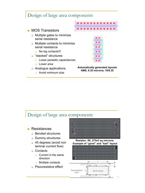
Design of large area components• MOS TransistorsMultiple gates to minimizeserial resistanceMultiple contacts to minimizeserial resistance No big contacts!!!“stacked” structures Lower parasitic capacitances Lower areaAnalogue applications Avoid minimum sizeAutomatically generated layoutsAMS, 0.35 microns, 10/0.35Design of large area components• ResistancesBended structuresDummy structures45 degrees (avoid nonlaminar current flow)Contacts Current in the samedirection Multiple contactsPiezoresistive effectResistor: 5K, 275x3 sq microns.Example of “good” and “bad” layout