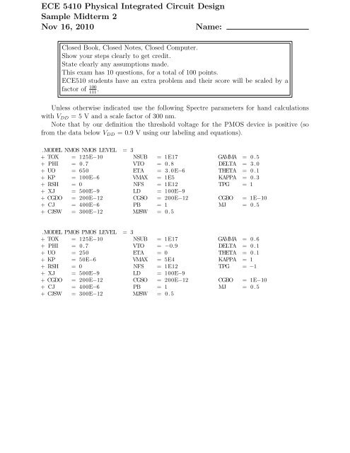
ECE 5410 Physical Integrated Circuit Design Sample Midterm 2 Nov ...
ECE 5410 Physical Integrated Circuit Design Sample Midterm 2 Nov ...
ECE 5410 Physical Integrated Circuit Design Sample Midterm 2 Nov ...

Create successful ePaper yourself
Turn your PDF publications into a flip-book with our unique Google optimized e-Paper software.
3. (20 points) Using 300n CMOS process data from problem 1, design a buffer to drive 20pF load with least delay. Also assume the approximated switching model of MOSFETswith C in = C out = C ox . Sketch the buffer schematic and label the sizes. Clearly showthe logical effort steps.Page 4
4. (10 points) Sketch, for a MOSFET with V DS = V DD , the log(I D ) against V GS . Indicateon your plot weak, moderate, and strong inversion. Also, indicate the MOSFET’sthreshold voltage and the subthreshold slope. What is the ideal subthreshold slope?Why?Page 5
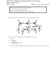
5. (10 points) Find the voltages at each of the nodes, A, B, C, D, E and F below. Use thecircuit parameters for the 300nm model given on the first page.VDDVDD VDD VDDFVDDA B C D EPage 6
6. (10 points) Show how to determine, using the square-law equations, the switching pointof a CMOS inverter. On an inverter’s voltage transfer curves show how changing theβ n /β p ratio shifts the curves up and down.Page 7
7. (10 points) Draw the schematic of a charge pump to generate approximately 3(V DD −V T HN ) output voltage.Page 8
8. (10 points) Explain with sketches, the body-effect and DIBL effect in a PMOS.Page 9
10. (11 points) Only for <strong>ECE</strong>510 students: Draw an implementation of a charge pumpto nearly 3V DD − V T HN output voltage, using an architecture to cancel the V T HN dropin the charge transfer devices.Page 11