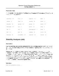
1 ECE 310L : L Read the lab assignment in its entirety. 1. For the ...
1 ECE 310L : L Read the lab assignment in its entirety. 1. For the ...
1 ECE 310L : L Read the lab assignment in its entirety. 1. For the ...

You also want an ePaper? Increase the reach of your titles
YUMPU automatically turns print PDFs into web optimized ePapers that Google loves.
<strong>ECE</strong> <strong>310L</strong> : LAB 10PRELAB ASSIGNMENT:<strong>Read</strong> <strong>the</strong> <strong>lab</strong> <strong>assignment</strong> <strong>in</strong> <strong>its</strong> <strong>entirety</strong>.<strong>1.</strong> <strong>For</strong> <strong>the</strong> circuit shown <strong>in</strong> Figure 3, compute a value for R1 that will result <strong>in</strong> a1N5230B zener diode current of approximately 5mA (you can ignore <strong>the</strong> effect ofbase current). Assume V<strong>in</strong> is 8V.OBJECTIVES:Construct and verify <strong>the</strong> operation of an NMOS unity ga<strong>in</strong> amplifier.Construct and verify <strong>the</strong> operation of a BJT unity ga<strong>in</strong> amplifier.Use an emitter follower/source follower to improve <strong>the</strong> load regulation of a zener diodevoltage regulator.MATERIALS:DC Power supplyOscilloscopeSignal GeneratorDMMSolderless breadboadHookup WireResistors: VariousCapacitors: 10uF, 100nFDiode: 1N5230BTransistors: ZVN3306A, 2N2222ABACKGROUND:Some amplifiers are design to act primarily as buffers, where <strong>the</strong>y isolate circu<strong>its</strong> byprovid<strong>in</strong>g high <strong>in</strong>put impedance while a voltage ga<strong>in</strong> of nearly one, or unity ga<strong>in</strong>. Thecommon-dra<strong>in</strong> NMOS amplifier shown <strong>in</strong> Figure 1 is one such amplifier, and iscommonly referred to as a source follower. The name source follower <strong>in</strong>dicates <strong>the</strong>output is taken from <strong>the</strong> source and is <strong>in</strong> phase with <strong>in</strong>put, i.e. V S “follows” V G . The termcommon dra<strong>in</strong> comes from <strong>the</strong> idea that <strong>the</strong> dra<strong>in</strong> is connected directly to V DD with noload resistance and <strong>in</strong> <strong>the</strong> AC analysis <strong>the</strong> supply rail, V DD , is a ground reference. Thevoltage ga<strong>in</strong> (A V ) of <strong>the</strong> source follower is <strong>in</strong>herently less than one and is generally <strong>in</strong><strong>the</strong> range 0.8 – 0.9. The current ga<strong>in</strong> can be much higher than one, though, allow<strong>in</strong>g <strong>the</strong>source follower to buffer between a high-impedance source and a low-impedance load.1
Figure 1A similar configuration that provides approximately unity ga<strong>in</strong> along with currentamplification is <strong>the</strong> BJT common-collector amplifier or <strong>the</strong> emitter follower. The emitterfollower is <strong>the</strong> BJT equivalent of <strong>the</strong> NMOS source follower. This <strong>lab</strong> will explore <strong>the</strong>operation of <strong>the</strong>se amplifiers and exam<strong>in</strong>e <strong>the</strong> ga<strong>in</strong> and phase response.Figure 22
The <strong>in</strong>put coupl<strong>in</strong>g capacitors are very large, so <strong>the</strong>ir poles will be near 0. The lowfrequency response of <strong>the</strong> system will thus be determ<strong>in</strong>ed by C 2 . The RC time constantwill set <strong>the</strong> cut-off frequency so <strong>in</strong> this design <strong>the</strong> significant time constant will be C 2 and<strong>the</strong> equivalent resistance seen by C 2 .In <strong>the</strong> NMOS amplifier <strong>the</strong> time constant will be determ<strong>in</strong>ed by <strong>the</strong> output capacitor, C 2 ,which is <strong>in</strong> series with <strong>the</strong> load resistor and <strong>the</strong> parallel comb<strong>in</strong>ation of <strong>the</strong> source1resistor and <strong>the</strong> impedance seen <strong>in</strong> <strong>the</strong> NMOS source, .gmVGS2IDVTN1 <strong>1.</strong>2k|| 100k100nFg m In <strong>the</strong> BJT amplifier, <strong>the</strong> time constant will be determ<strong>in</strong>ed by <strong>the</strong> output capacitor, C 2 ,which is <strong>in</strong> series with <strong>the</strong> load resistor and <strong>the</strong> parallel comb<strong>in</strong>ation of <strong>the</strong> emitterresistor and <strong>the</strong> impedance seen <strong>in</strong> <strong>the</strong> BJT emitter, r e .1 rTHre , wheregm1 4.7k|| 4.7kre 40I200 1 470 || 40IccgmVITCg m4.7k|| 4.7k 100k100nF200 Then, you will use <strong>the</strong> NMOS source follower and <strong>the</strong> BJT emitter followerconfigurations to help improve <strong>the</strong> l<strong>in</strong>e/load regulation of a zener diode voltage regulatorand allow for higher load current. The BJT version of this circuit is shown <strong>in</strong> Figure 3.Figure 3SETUP:Turn on power to <strong>the</strong> DMM, oscilloscope, power supply, and signal generator. Set <strong>the</strong>power supply +25V current limit to 100mA.3
Pay careful attention to <strong>the</strong> transistor p<strong>in</strong>-out as shown below to avoid damag<strong>in</strong>g <strong>the</strong>m.ZVN3306A p<strong>in</strong>-out2N2222A p<strong>in</strong>-outLAB ASSIGNMENT:<strong>1.</strong> Use <strong>the</strong> DMM to measure <strong>the</strong> values of <strong>the</strong> resistors. Use <strong>the</strong> measuredcomponent values <strong>in</strong> your calculations.2. Construct <strong>the</strong> circuit shown <strong>in</strong> Figure <strong>1.</strong> Connect <strong>the</strong> oscilloscope to measure <strong>the</strong><strong>in</strong>put and V OUT .3. Measure and record <strong>the</strong> operat<strong>in</strong>g po<strong>in</strong>t of <strong>the</strong> transistor (I D , V DS ). Note that<strong>the</strong>re is no dra<strong>in</strong> resistor to permit easy measurement of I D , but you canmeasure I S .4. Measure and plot <strong>the</strong> ga<strong>in</strong> and phase characteristics of <strong>the</strong> amplifier from 10Hzto 100kHz. Use a 1Vpp s<strong>in</strong>usoid as <strong>the</strong> <strong>in</strong>put.5. Increase <strong>the</strong> <strong>in</strong>put signal peak-to-peak voltage until <strong>the</strong> output signal becomesdistorted or clips. What are <strong>the</strong> <strong>in</strong>put and output voltage levels at this po<strong>in</strong>t? Howdo <strong>the</strong>se voltages relate to <strong>the</strong> bias po<strong>in</strong>t of <strong>the</strong> amplifier?6. Construct <strong>the</strong> circuit shown <strong>in</strong> Figure 2.7. Measure and record <strong>the</strong> operat<strong>in</strong>g po<strong>in</strong>t of <strong>the</strong> transistor (I C , V CE ). Note that<strong>the</strong>re is no collector resistor to permit easy measurement of I C , but you canmeasure I E .8. Measure and plot <strong>the</strong> ga<strong>in</strong> and phase characteristics of <strong>the</strong> amplifier from 10Hzto 100kHz. Use a 1Vpp s<strong>in</strong>usoid as <strong>the</strong> <strong>in</strong>put.9. Increase <strong>the</strong> <strong>in</strong>put signal peak-to-peak voltage until <strong>the</strong> output signal becomesdistorted or clips. What are <strong>the</strong> <strong>in</strong>put and output voltage levels at this po<strong>in</strong>t? Howdo <strong>the</strong>se voltages relate to <strong>the</strong> bias po<strong>in</strong>t of <strong>the</strong> amplifier?10. Construct <strong>the</strong> circuit shown <strong>in</strong> Figure 3. Set V<strong>in</strong> to 8V. Use a value for R1 that willresult <strong>in</strong> a 1N5230B zener diode current of approximately 5mA (you can ignore<strong>the</strong> effect of base current). Use 10kΩ for <strong>the</strong> <strong>in</strong>itial load resistor (this will beconsidered <strong>the</strong> no-load condition).4
1<strong>1.</strong> Measure <strong>the</strong> output voltage V REG .12. Add a parallel load resistor that will <strong>in</strong>crease <strong>the</strong> output current to approximately25 mA. Measure <strong>the</strong> output voltage V REG .13. Add a parallel load resistor that will <strong>in</strong>crease <strong>the</strong> output current to approximately50 mA. Measure <strong>the</strong> output voltage V REG .14. Leave <strong>the</strong> load set to approximately 50mA, and reduce V<strong>in</strong> to 7.2V. Measure <strong>the</strong>output voltage V REG .15. Increase V<strong>in</strong> to 8.8V. Measure <strong>the</strong> output voltage V REG .16. Replace <strong>the</strong> BJT with <strong>the</strong> NMOS FET, and repeat steps 10-15.REPORT:Write your report per <strong>the</strong> criteria <strong>in</strong> <strong>the</strong> syl<strong>lab</strong>us and <strong>the</strong> sample <strong>lab</strong> report posted on<strong>the</strong> course web page.In your report, also answer <strong>the</strong> questions below;<strong>1.</strong> Plot your ga<strong>in</strong> (dB) and phase measurements versus <strong>the</strong> <strong>in</strong>put frequency. Use alogarithmic scale for frequency.2. How does <strong>the</strong> measured low-frequency response of <strong>the</strong> amplifiers compared to<strong>the</strong> expected values?3. Compare <strong>the</strong> performance of <strong>the</strong> voltage regulators to each o<strong>the</strong>r. Calculate l<strong>in</strong>eand load regulation for both regulator configurations.5