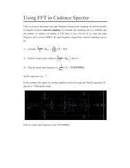
Assignment 3.pdf
Assignment 3.pdf
Assignment 3.pdf

You also want an ePaper? Increase the reach of your titles
YUMPU automatically turns print PDFs into web optimized ePapers that Google loves.
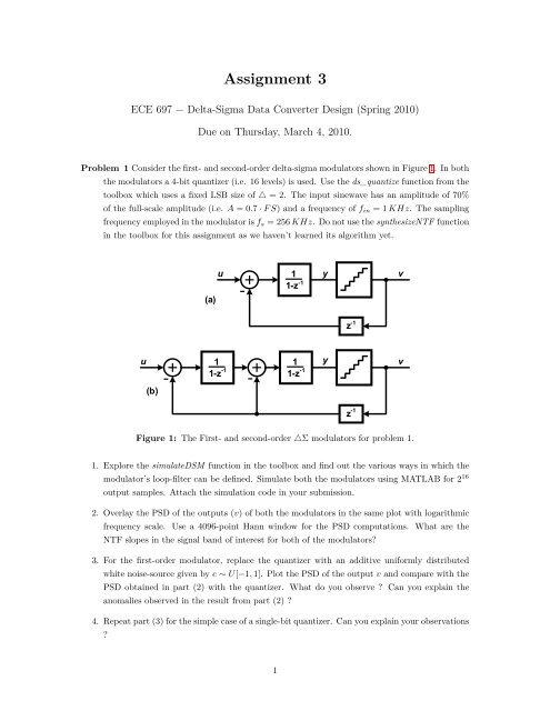
<strong>Assignment</strong> 3ECE 697 − Delta-Sigma Data Converter Design (Spring 2010)Due on Thursday, March 4, 2010.Problem 1 Consider the first- and second-order delta-sigma modulators shown in Figure 1. In boththe modulators a 4-bit quantizer (i.e. 16 levels) is used. Use the ds_quantize function from thetoolbox which uses a fixed LSB size of △ = 2. The input sinewave has an amplitude of 70%of the full-scale amplitude (i.e. A = 0.7 · F S) and a frequency of f in = 1 KHz. The samplingfrequency employed in the modulator is f s = 256 KHz. Do not use the synthesizeNTF functionin the toolbox for this assignment as we haven’t learned its algorithm yet.u1 y1-z -1(a)z -1u 11 y1-z -1 1-z -1(b)z -1vvFigure 1: The First- and second-order △Σ modulators for problem 1.1. Explore the simulateDSM function in the toolbox and find out the various ways in which themodulator’s loop-filter can be defined. Simulate both the modulators using MATLAB for 2 16output samples. Attach the simulation code in your submission.2. Overlay the PSD of the outputs (v) of both the modulators in the same plot with logarithmicfrequency scale. Use a 4096-point Hann window for the PSD computations. What are theNTF slopes in the signal band of interest for both of the modulators?3. For the first-order modulator, replace the quantizer with an additive uniformly distributedwhite noise-source given by e ∼ U[−1, 1]. Plot the PSD of the output v and compare with thePSD obtained in part (2) with the quantizer. What do you observe ? Can you explain theanomalies observed in the result from part (2) ?4. Repeat part (3) for the simple case of a single-bit quantizer. Can you explain your observations?1
ECE 697 - Delta-Sigma Data Converter Design (Spring 2010): <strong>Assignment</strong> 35. To avoid the problem observed in part (3), we can dither the quantizer input. Dither involvesadding a small amount of random noise source at the quantizer input. Repeat part (2) above,by adding a Gaussian distributed white dither noise given by d ∼ n(0, 0.1) (i.e. zero meanand with a standard deviation of σ = 0.1) at the quantizer input. What do you observe in thePSD now compared to what you saw for part (2) ? How does this PSD plot compare with theone seen in part (3) ?For further reading, details on dithering in delta-sigma modulators can be found in Chapter 3 ofreference [2].Problem 2 Decimation Filters: In this problem we will analyze and simulate the degradation inthe ideal performance of the delta-sigma modulator due to a poor decimation filter. Considerthe setup shown in Figure 2. Here, a delta-sigma modulator employing an oversampling ratio ofOSR is excited by a signal with maximum frequency content at a frequency f B . The modulatoris followed by a digital decimation filter. The output rate of the modulator is decimated by afactor equal to OSR. The modulator internally employs a quantizer introducing a uniformlydistributedwhite quantization noise e[n] with its variance given by σe.2u∆ΣModulatorvOSRv outBW=f Bf s =2f B OSRDecimationFilterFigure 2: A △Σ modulator followed by the decimation filter.1. Consider a first-order delta-sigma modulator (with NT F (z) = 1 − z −1 ) be followed by a Sincdecimation filter. The impulse response of the Sinc filter is given asFor this problem setup, we have N = OSR.⎧⎨ 1Nh 1 [n] =, 0 ≤ n ≤ N − 1⎩0, otherwise(a) Find the transfer function H 1 (z) of the Sinc filter and sketch its magnitude response∣ H1 (e jω ) ∣ ∣ .(b) Sketch the DTFT spectra at all the block outputs. Use ω as the variable on the frequencyaxis.(c) Show that the resulting quantization noise power (i.e the variance) σ 2 q1 at the output v outis given byσ 2 q1 =(1)2σ2 eOSR 2 (2)2
ECE 697 - Delta-Sigma Data Converter Design (Spring 2010): <strong>Assignment</strong> 3How does this compare with the resulting noise power when an ideal brick-wall filter isused with a cut-off frequency ofπOSR ?(d) How will you implement this decimation filter using discrete-time accumulator and combfilters? What is the droop in the signal band at f = f B ?(e) Plot the resultant spectrum for the noise at the block outputs by using/modifying thefollowing MATLAB script :% Creating NTF(z) = 1-z^-1b = [1 -1]; a = 1;NTF = dfilt.df2t(b,a);% Sinc filter of length 8, H1N = 8; b1 = [1 0 0 0 0 0 0 -1]/N;a1 = [1 -1];H1=dfilt.df2t(b1,a1);% Cascade of NTF followed by H1Hcas=dfilt.cascade(NTF,H1);% Plotsfvtool(NTF, H1, Hcas);2. Now, in order to increase the effectiveness of the decimation filter and reduce the quantizationnoise aliased into the signal band, a Sinc 2 digital filter is employed.The transfer function ofthe Sinc 2 filter is given by[ (1) ] 21 − z−NH 2 (z) =N (1 − z −1 (3))(a) Sketch its magnitude response ∣ ∣H 2 (e jω ) ∣ ∣. Can you find the impulse response h 2 [n] of theSinc 2 filter ?(b) Sketch the DTFT spectra at all the block outputs and compare with your MATLABplots. Use ω as the variable on the frequency axis.(c) Show that the resulting quantization noise power σ 2 q2 at the output v out is given byσ 2 q2 =2σ2 eOSR 3 (4)How does this compare with the resulting noise power when an ideal brick-wall filter isused with a cut-off frequency ofπOSR ?(d) How will you implement this decimation filter using discrete-time accumulator and combfilters? What is the droop in the signal band at f = f B ?3. Now, consider a second-order delta-sigma modulator (with NT F (z) = ( 1 − z −1) 2) be followedby the Sinc decimation filter.(a) Sketch the DTFT spectra at all the block outputs and compare it with MATLAB generatedplots.3
ECE 697 - Delta-Sigma Data Converter Design (Spring 2010): <strong>Assignment</strong> 3(b) Find an expression for the resulting quantization noise power σ 2 q1 at the output v out ?How does this compare with the resulting noise power when an ideal brick-wall filter isused with a cut-off frequency ofπOSR ?(c) Repeat parts (a) and (b) when a Sinc 2 digital filter is used.(d) Repeat parts (a) and (b) when a Sinc 3 digital filter is employed. The transfer functionof the Sinc 3 function is given by[ (1) ] 31 − z−NH 3 (z) =N (1 − z −1 (5))(e) How much is the signal droop at f = f B ? From the above exercise what can you intuitabout the cut-off rate of the decimation filter when compared to the modulator’s responseat frequencies near f = f B ?In practice, the decimation filtering scheme required for high-resolution higher-order modulatorsis more complicated than a simple cascade of Sinc filters. FIR filters are usually employedin the decimation chain to compensate for the droop due to the Sinc k filter. For details referto Section 3.5 of the textbook. For a practical example of decimation filtering scheme refer topage 21 of the reference [3].Hint: You may find the following definite integrals usefulπ∫20∫ π0∫ π0( ) Nxsin 4 dx = 3π 2 8( ( x) ( )) 2 Nxsin sin dx = π 2 24( sin M+1 ) 2(Nx)dx = πN sin (x)2( M∏m=1)2m − 12m(6)(7)(8)4
ECE 697 - Delta-Sigma Data Converter Design (Spring 2010): <strong>Assignment</strong> 3Bonus Problem: Half-Band Filters: Read the reference [4] and the Delta-Sigma Toolbox documentationfor the functions designHBF and simulateHBF used for designing linear-phasehalf-band FIR filters employed in the decimation filter chain.1. Understand what these functions perform and demonstrate the usage in designing hardwareefficient half-band filters.2. Using MATLAB implement the decimation filter chain for the specifications seen in the AD9262datasheet (see ref [3]). Assume that the signal bandwidth of the ADC is 10 MHz.References:[1] S. Pavan, N. Krishnapura, EE658: Data Conversion Circuits Course, IIT Madras. Available:[Online] http://www.ee.iitm.ac.in/vlsi/courses/ee658_2009/start.[2] S. R. Norsworthy, R. Schreier, G. C. Temes, Delta-Sigma Data Converters: Theory, Design, andSimulation, Wiley-IEEE Press, 1996 (the Yellow Book of Delta-Sigma Converters).[3] A 16-bit, 2.5MHz/5 MHz/10 MHz, 30 MSPS to 160 MSPS Dual Continuous Time Sigma-DeltaADC – AD9262, Analog Devices, 2008. Available: AD9262 Datasheet.[4] T. Saramäki, “Design of FIR filters as a tapped cascaded interconnection of identical subfilters,”IEEE Transactions on Circuits and Systems, vol. 34, pp. 1011-1029, 1987.5