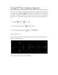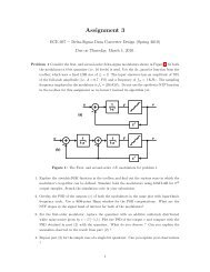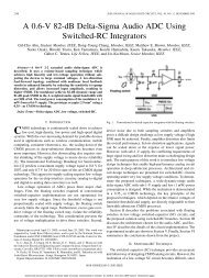
ECE614 CMOS Analog IC Design HW1
ECE614 CMOS Analog IC Design HW1
ECE614 CMOS Analog IC Design HW1

You also want an ePaper? Increase the reach of your titles
YUMPU automatically turns print PDFs into web optimized ePapers that Google loves.
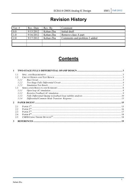
<strong>ECE614</strong> <strong>CMOS</strong> <strong>Analog</strong> <strong>IC</strong> <strong>Design</strong> <strong>HW1</strong> Fall 2012Revision HistoryVer. # Rev. Date Rev. By Comment0.0 9/15/2012 Kehan Zhu Initial draft1.0 9/16/2012 Kehan Zhu Remove class A part2.0 9/17/2012 Kehan Zhu Comments and problem 2 addedContents1 TWO-STAGE FULLY-DIFFERENTIAL OPAMP DESIGN .............................................................................. 31.1 SPEC. AND REQUIREMENT ................................................................................................................................... 31.2 CIRCUIT DESIGN AND TEST BENCH ..................................................................................................................... 31.2.1 Bias Circuit ................................................................................................................................................. 31.2.2 Two-Stage Fully Differential Circuit .......................................................................................................... 41.2.3 Simulation Test Bench................................................................................................................................. 51.3 SIMULATION RESULTS AND SUMMARY ................................................................................................................ 81.3.1 Open loop AC simulation ............................................................................................................................ 81.3.2 Resistive Feedback AC simulation .............................................................................................................. 91.3.3 Fully Differential Opamp in feedback loop stability analysis ................................................................... 101.3.4 Differential/Common Mode Transient Response ..................................................................................... 132 PAPER DIGEST ..................................................................................................................................................... 152.1 PAPER 1 [1] .......................................................................................................................................................... 152.2 PAPER 2 [2] .......................................................................................................................................................... 162.3 PAPER 3 [3] .......................................................................................................................................................... 172.4 PAPER 4 [4] .......................................................................................................................................................... 182.5 CMFB USING TRIODE DEV<strong>IC</strong>ES [5] ..................................................................................................................... 183 REFERENCES ....................................................................................................................................................... 19Kehan Zhu1
<strong>ECE614</strong> <strong>CMOS</strong> <strong>Analog</strong> <strong>IC</strong> <strong>Design</strong> <strong>HW1</strong> Fall 2012Table of FiguresFigure 1 Bias generation circuit schematic. ....................................................................................................... 3Figure 2 Schematic of 2-stage fully differential circuit with class AB output stage. .......................................... 5Figure 3 Two-stage common-mode picture. ...................................................................................................... 5Figure 4 Closed loop stability analysis test bench. ............................................................................................ 6Figure 5 Closed loop stb analysis test bench using cmdmprobe. ..................................................................... 6Figure 6 Differential open loop AC simulation test bench. ................................................................................ 6Figure 7 Differential closed loop AC simulation test bench. .............................................................................. 7Figure 8 Unity-gain inverter transient simulation test bench for differential mode step response..................... 7Figure 9 Unity-gain inverter transient simulation test bench for common mode step response. ...................... 7Figure 10 Differential open loop bode plot. ....................................................................................................... 8Figure 11 Close loop AC simulation bode plot and summary. .......................................................................... 9Figure 12 Close loop AC simulation magnitude plot when configured at unity-gain. ...................................... 10Figure 13 First stage CMFB stb analysis with cmdmprobe. ............................................................................ 10Figure 14 First stage CMFB stb analysis with iprobe. ..................................................................................... 11Figure 15 Second stage CMFB stb analysis with cmdmprobe. ....................................................................... 11Figure 16 Second stage CMFB stb analysis with iprobe. ................................................................................ 12Figure 17 Two-stage class A closed loop stb analysis with cmdmprobe. ....................................................... 12Figure 18 Closed loop bode plot configured as unity gain inverter using cmdmprobe stb analysis. ............... 13Figure 19 Unity- gain inverting amplifier transient response with a 200mV differential step (rise/falltime=0.1ns, pulse with=100ns, in test bench set output VCVS gain=-1). ................................................ 14Figure 20 Unity- gain inverting amplifier transient response with a 100mV common mode step (rise/falltime=0.1ns, pulse with=100ns, in the test bench veriloga adder is used for averaging). ........................ 14Figure 21 Operational amplifier used in the first integrator. (a) Main amplifier. (b) Common-mode feedback(CMFB) for the first stage. (c) Second-stage CMFB circuit. ..................................................................... 15Figure 22 Schematic of the operational amplifier used in the second and third integrators and the summingamplifier. ................................................................................................................................................... 16Figure 23 Operational amplifier used in the first integrator in paper 2. ........................................................... 16Figure 24 Feedforward compensated opamp used in the paper 3. Feedforward path is shown in bold, andCMFB paths are shown in gray. ............................................................................................................... 17Figure 25 Feedforward compensated opamp used in the summing amplifier. Feedforward path is shown inbold, and CMFB paths are shown in gray. ............................................................................................... 17Figure 26 Feedforward opamp schematic, including common-mode feedback. ............................................. 18Figure 27 CMFB using triode devices. ............................................................................................................ 18List of tablesTable 1 Summary and comparison of stb analysis for the three feedback loops at tt corner. ........................ 13Kehan Zhu2
<strong>ECE614</strong> <strong>CMOS</strong> <strong>Analog</strong> <strong>IC</strong> <strong>Design</strong> <strong>HW1</strong> Fall 20121 Two-stage fully-differential Opamp design1.1 Spec. and Requirement Process: IBM 130nm <strong>CMOS</strong>, 1.2V nominal power supply voltage. Specification: Closed loop gain and -3dB bandwidth are 2 and 20MHz, respectively.CC LL = 5pppp. Rail-to-rail output swing. Open loop gain 70dB. VV CCCC = VV DDDD /2. Requirements: individual CMFB loops; No systematic offset in CMFB loops; Compensateall the three feedback loops for PM of 60º. Pass tt and ssf corners. Simulation list:1. Differential open loop gain-magnitude and phase. Indicate the phase margin.2. Differential closed loop gain-magnitude and phase. Indicate the -3 dB bandwidth.3. First stage common-mode loop gain-magnitude and phase. Indicate the phase margin.4. Second stage common-mode loop gain-magnitude and phase. Indicate the phase margin.5. Transient response of the unity-gain inverting amplifier with a 200 mV differential step(use 0.1 ns rise/fall times).6. Transient response of the unity-gain inverting amplifier with a 100 mV common modestep (use 0.1 ns rise/fall times).1.2 Circuit <strong>Design</strong> and Test BenchIn order to go through the CFMB and compensation theory, Class A output is first designed.Then Class AB output stage is implemented. Here, only class AB topology result is shown.ADE XL is used to do corner simulation. Schematic simulation are performed at 1.2V powersupply, 40ºC temperature, tt and ssf corners.1.2.1 Bias CircuitBias circuit generates voltages for vb1, vb2, vb3, vb4 used to bias the current source/sinkused in the fully differential opamps. Assume we get a reference voltage of 600mV and a 10µA@27ºC PTAT current from BGR. As a rule of thumb, set the temperate coefficient of thePTAT current to be 0.067µA/ºC in the simulation.A regulated current reference with external precision 60K Ohm resistor to generate a 10µAcurrent into high swing current source to generate bias voltages for the opamp.20/0.812/0.812/0.86/0.85/1.528/0.358/0.354/0.354/0.35Id=10µ+(temp-27)*0.067200/0.825/0.5ESD sensitivenode10/0.35/1.55/0.310/1 20/110/1.55/55/1.5External res ¶sitic capFigure 1 Bias generation circuit schematic.Kehan Zhu3
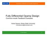
<strong>ECE614</strong> <strong>CMOS</strong> <strong>Analog</strong> <strong>IC</strong> <strong>Design</strong> <strong>HW1</strong> Fall 20121.2.2 Two-Stage Fully Differential CircuitOpamp topology:Folded-cascode opamp topology is chosen as the first stage for 1.2V nominal power supplyand to obtain high DC gain. Class AB output stage is used to extend the signal swing.Separate CMFB scheme is used for both stages to set each output to well defined commonmode voltage level, here is 600mV. The quiescent output voltage at nodes vop1 and von1sets the quiescent currents in the second stage [1] .Look at the common mode picture as shown in Fig 3, at high frequencies, the 2 nd -stagecompensation capacitor 2CC CC can be considered as short, the common mode outputimpedance of the class AB consists of the parallel combination of the positive resistance ofthe diode connected (through 2CC CC ) transistor M8 and the negative resistance formed by theloop M4-M6-M7. In the presence of mismatches, it is possible for the common mode outputimpedance to have a negative real part and lead to instability. To prevent this and ensurestability and reliable operation of the CMFB loop, quiescent current in the upper PMOS,which contributes to the positive resistance, should be made larger than quiescent current inthe lower NMOS [1] . My design missed this point!CMFB topology:Since the output swings of the first stage is modest in closed loop applications, the linearityof the common mode detector is not critical [1] . we can use Dual-Diff amp scheme to mergethe CM detector and the error amplifier as a one. And it doesn’t load the first stage thatmuch.For class AB output stage, since the signal swings are large, linear operation of the CMFBmechanism is ensured by using resistive averaging to detect the output common mode.Parallel cap is added to form high frequency path to cancel the pole introduced by theparasitic cap of the error amplify input pair. The resistor should be large enough to ensurehigh output impedance. The feedback node is acting as a VCCS to control the gate of aPMOS by injecting current to tune output common mode level.Compensation:There are two internal common mode feedback loops and one external feedback loop, sothat the circuit should be compensated to ensure stability. For the 2-stage opamp and 1 st -stage CMFB loop, miller compensation is simply used.The 2 nd -stage CMFB loop is also a 2-stage opamp as can be clearly seen in the CM pictureillustrated in Fig 3. In order to make sure the loop is stable and avoid using miller caploading the output, I just change the load of the error amplify to diode connected, make itone pole system but sacrifice the gain. Actually, it may be better to use miller compensationfor higher gain and smaller systematic offset introduced by matching. But I have limitedtime to go back and re-simulate.Minimize systematic offset:The current density in the error amplify should be matched to the current density in the mainstage opamp. The gates bias of current source of the second stage CMFB error amplify aretied as shown in Fig2. Since it’s diode connected load, the W/L of the PMOS load is a littledifferent with the W/L of the feedback controlled PMOS.Kehan Zhu4
<strong>ECE614</strong> <strong>CMOS</strong> <strong>Analog</strong> <strong>IC</strong> <strong>Design</strong> <strong>HW1</strong> Fall 201250µ 50µ4II OOII OOvcmfb2 12/0.548/0.512/0.5von5/1.6vbn_l10/0.460/0.88/0.35vop110/0.350/0.4 10/1.5vcmfb1vp160/0.580/0.380/1.5vcmfb1vnvon1vbn_r12/0.8vcmfb22/0.5vop12/0.8242Kvcmfb1 vcmfb2300K4/0.52/0.54/0.54/0.520/0.3vbn_lvbn_r20/1.5 10/0.4153f5II OOII OO10µ 80µ10µ II OO 5II OO20µ2II OO1 st -stage CMFB 2 nd -stage CMFB13K 680fbias1.03K 2pvop1 von von1 vopvop1vcmfb1von1Miller compensation for 2 nd -stage opampMiller compensation for 1 st -stage CMFBFigure 2 Schematic of 2-stage fully differential circuit with class AB output stage.Loop 1M4M9M8Incorrect place to insert iprobeRR ZZ /2 2CC CCM5M6M7Loop 2Figure 3 Two-stage common-mode picture.1.2.3 Simulation Test BenchOpen loop and closed loop frequency analysis are performed by AC simulation.Fig 4 is used to perform stability analysis for common mode loop and closed loop of thefully differential opamp. For CMFB loop, usually there have two places can break the loop,which are differential input sensing nodes or single-ended control node at the output of theerror amplify. For differential nodes, we use cmdmprobe and set CMDM=1, for singleendednode, we simply use iprobe. One thing worth to mention is that, if probe is placedbetween two high impedance nodes, results obtained by using cmdmprobe and iprobe are allthe same (eg. Loop 1). While, for loop 2, the output of the error amplifier is not a highimpedance node, so that it’s not correct to use iprobe (indicated in Fig 4) for the secondstage CMFB stability analysis.Differential mode and common mode transient responses are checked in the end.Kehan Zhu5
<strong>ECE614</strong> <strong>CMOS</strong> <strong>Analog</strong> <strong>IC</strong> <strong>Design</strong> <strong>HW1</strong> Fall 2012vcmfb1vcmfb1vcmfb2vcmfb2vcmfb1vonvop1vpvnvon1vop1von1vopvcmfb2Low impedance nodevopvonvnvpvopvonvop1 von von1 vopvop1von1vcmfb1biasThe 2-stage opamp schematic inside the symbol is shown right aboveFigure 4 Closed loop stability analysis test bench.Figure 5 Closed loop stb analysis test bench using cmdmprobe.Figure 6 Differential open loop AC simulation test bench.Kehan Zhu6
<strong>ECE614</strong> <strong>CMOS</strong> <strong>Analog</strong> <strong>IC</strong> <strong>Design</strong> <strong>HW1</strong> Fall 2012Figure 7 Differential closed loop AC simulation test bench.Figure 8 Unity-gain inverter transient simulation test bench for differential mode step response.Figure 9 Unity-gain inverter transient simulation test bench for common mode step response.Kehan Zhu7
<strong>ECE614</strong> <strong>CMOS</strong> <strong>Analog</strong> <strong>IC</strong> <strong>Design</strong> <strong>HW1</strong> Fall 20121.3 Simulation Results and SummarySimulation results are obtained with the test benches described above. First, by using DCand AC simulation to check the DC node voltages and open loop opamp specifications. Inresistive feedback AC simulation, as shown in Fig11, the calculator expression seems notmatch the bode plot.Then, closed loop stability analysis is followed to ensure the three feedback loops in thesystem are stable. Last, transient simulation is performed to see the differential and commonmode responses.In conclusion, all simulation under 40ºC, 1.2V power supply, ssf and tt corner, the open loopDC gain is higher than 70dB. Table 1 summarized and compared the aforementioned threeloops by using cmdmprobe and iprobe stb analysis. It shows that for CMFB loop 2, iprobe isnot accurate due to low impedance node, its PM got from cmdmprobe seems too large and itshould be improved later on .DC current consumption of the fully differential opamp at ssf and tt corner is 1.35mA and1.86mA, respectively, all at 1.2V power supply and 40ºC.1.3.1 Open loop AC simulationFigure 10 Differential open loop bode plot.Kehan Zhu8
<strong>ECE614</strong> <strong>CMOS</strong> <strong>Analog</strong> <strong>IC</strong> <strong>Design</strong> <strong>HW1</strong> Fall 20121.3.2 Resistive Feedback AC simulationFigure 11 Close loop AC simulation bode plot and summary.Kehan Zhu9
<strong>ECE614</strong> <strong>CMOS</strong> <strong>Analog</strong> <strong>IC</strong> <strong>Design</strong> <strong>HW1</strong> Fall 2012Figure 12 Close loop AC simulation magnitude plot when configured at unity-gain.1.3.3 Fully Differential Opamp in feedback loop stability analysisWhen analysis common mode loop stability, CMDM should be set as 1 in the cmdmprobeproperty.For first stage CMFB loop, the results obtained by using cmdmprobe and iprobe match quitewell (refer to Fig 13 and Fig 14).While, for the second stage CMFB loop, the results got by using different probes aredifferent (see Fig.15 and Fig 16) due the low impedance node at output of the 2 nd stage erroramplifier as shown in Fig 4.Figure 13 First stage CMFB stb analysis with cmdmprobe.Kehan Zhu10
<strong>ECE614</strong> <strong>CMOS</strong> <strong>Analog</strong> <strong>IC</strong> <strong>Design</strong> <strong>HW1</strong> Fall 2012Figure 14 First stage CMFB stb analysis with iprobe.Figure 15 Second stage CMFB stb analysis with cmdmprobe.Kehan Zhu11
<strong>ECE614</strong> <strong>CMOS</strong> <strong>Analog</strong> <strong>IC</strong> <strong>Design</strong> <strong>HW1</strong> Fall 2012Figure 16 Second stage CMFB stb analysis with iprobe.Figure 17 Two-stage class A closed loop stb analysis with cmdmprobe.Kehan Zhu12
<strong>ECE614</strong> <strong>CMOS</strong> <strong>Analog</strong> <strong>IC</strong> <strong>Design</strong> <strong>HW1</strong> Fall 2012Table 1 Summary and comparison of stb analysis for the three feedback loops at tt corner.Items DC Gain (dB) PM (º) GBW (MHz) stb options81.91 62.81 19.88 CMDM=11 st stage CMFB NA NA NA CMDM=-181.91 62.8 19.88 iprobe18.58 90.44 32.08 CMDM=12 nd stage CMFB NA NA NA CMDM=-118.58 56.34 123.2 Misused iprobeClosed loop-106.07 NA NA CMDM=167.53 68.67 14.87 CMDM=-1When it configured as unity-gain feedback, the phase margin drops!Figure 18 Closed loop bode plot configured as unity gain inverter using cmdmprobe stb analysis.1.3.4 Differential/Common Mode Transient ResponseTransient simulations are performed to test differential mode and common mode responseswhen the opamp is configured in unity gain with resistive feedback. 200mV differentialpulse and 100mV common mode pulse with 0.1ns rise/fall times and 100ns pulse width aresimulated, resulting waveforms are plotted in Fig 19 and Fig 20, respectively.For differential mode response, as shown in Fig 19, there is a overshoot and undershootabout 40mV, and the slew rate is limited due to 5pF load. The under damping maybe causedby less phase margin when configured to unity-gain.For common mode response, as shown in Fig 20, the common mode disturbance at the inputis attenuated by more than 40dB at ssf corner.Kehan Zhu13
<strong>ECE614</strong> <strong>CMOS</strong> <strong>Analog</strong> <strong>IC</strong> <strong>Design</strong> <strong>HW1</strong> Fall 2012Figure 19 Unity- gain inverting amplifier transient response with a 200mV differential step (rise/falltime=0.1ns, pulse with=100ns, in test bench set output VCVS gain=-1).Figure 20 Unity- gain inverting amplifier transient response with a 100mV common mode step(rise/fall time=0.1ns, pulse with=100ns, in the test bench veriloga adder is used for averaging).Kehan Zhu14
<strong>ECE614</strong> <strong>CMOS</strong> <strong>Analog</strong> <strong>IC</strong> <strong>Design</strong> <strong>HW1</strong> Fall 20122 Paper DigestFor each of the example common-mode feedback loop designs shown in the CMFBExamples handout: Explain the operation of the CMFB loops in both the opamp stages, andcomment on their relative advantages and disadvantages.2.1 Paper 1 [1]Figure 21 Operational amplifier used in the first integrator. (a) Main amplifier. (b) Common-modefeedback (CMFB) for the first stage. (c) Second-stage CMFB circuit.Telescopic cascode opamp with class AB output stage.1 st -stage CMFB is dual diff-amp topology.‣ Pros:Eliminating large resistors; less loading introduced to the main opamp; Commonmodedetector and error amplifier as a one.‣ Cons :Large signal swings will cause linearity issue.2 nd -stage CMFB is resistive averaging common-mode detector with output voltage fromerror amplifier to control the current of common-source PMOS injecting to the fullydifferential outputs.‣ Pros:Resistive detector can sense large signal swings to alleviate linearity issue to theKehan Zhu15
<strong>ECE614</strong> <strong>CMOS</strong> <strong>Analog</strong> <strong>IC</strong> <strong>Design</strong> <strong>HW1</strong> Fall 2012error amplifier; clever way to use current to adjust the output common-mode level sothat each stage can do CMFB separately.‣ Cons :Resistors should be large enough that will occupy considerable silicon areas; thegate(biasn3) of NMOS current source of the error amplifier is not a replica of thesecond-stage quiescent current so that current densities may not be well matched andsystematic offset will be introduced in the CMFB loop.Figure 22 Schematic of the operational amplifier used in the second and third integrators and thesumming amplifier.NMOS input version, second stage CMFB is similar with the previous one. Two diodeconnectedNMOS transistors (M6 and M7) are stacked to increase the drain voltage at M5,make it better matches with the quiescent current in the second stage CMFB error amplifier.One potential problem is that the first stage CMFB is not an exactly replica of the first stageof the main opamp which may cause systematic offset for the CMFB loop of the first stage.2.2 Paper 2 [2]Figure 23 Operational amplifier used in the first integrator in paper 2.Feedforward compensation with clever first stage CMFB, it uses transistors (M5 and M6) todetect common-mode voltage and sources a portion of current from the tail current of thefirst stage main opamp. MM 5,6 are replicas of MM 9.10 and operate in saturation region. Since theKehan Zhu16
<strong>ECE614</strong> <strong>CMOS</strong> <strong>Analog</strong> <strong>IC</strong> <strong>Design</strong> <strong>HW1</strong> Fall 2012gate voltages of MM 9.10 and MM 5,6 are the same. In order to let MM 9.10 and MM 5,6 have the sameVV DDDD , diode-connected transistor M7 (indicate in red circle) is inserted to match the M7 in thesecond stage.‣ Pros:Very compact CMFB scheme for the first stage; second stage current is reused forfeedforward compensation which achieves higher unity gain frequency than millercompensation for a given power.‣ Cons :The first stage common-mode level may not be well defined since there is noreference voltage to be compared in the feedback loop; the feedforward transistorsMM 7.8 connected between input and output nodes which restricts the differential peakto-peakoutput swing to four time the threshold voltage.2.3 Paper 3 [3]Figure 24 Feedforward compensated opamp used in the paper 3. Feedforward path is shown in bold,and CMFB paths are shown in gray.This is basically the same topology as proposed in paper 2. For the left one, transistorsMM cc1.cc2 are augmented act as a low-impedance nodes for high frequencies.Figure 25 Feedforward compensated opamp used in the summing amplifier. Feedforward path isshown in bold, and CMFB paths are shown in gray.Kehan Zhu17
<strong>ECE614</strong> <strong>CMOS</strong> <strong>Analog</strong> <strong>IC</strong> <strong>Design</strong> <strong>HW1</strong> Fall 2012The feedforward stage is modified to have two stages, a low gain high speed stage M 5,6followed by common source amplifiers M 7,8 , in order to support high output swing. Thelatter permits a high output swing while the former provides common mode rejection.2.4 Paper 4 [4]Figure 26 Feedforward opamp schematic, including common-mode feedback.This is a three-stage fully differential opamp with two feedforward stages for compensation.A small current is injected into each common-mode feedback summing node to raise thecommon-mode level at extreme cases.‣ Pros:Simple local common-mode feedbacks save power.‣ Cons :No flexibility to set the output common mode; small resistors lower the gain whilelarge resistors occupy area; feedforward amplifier burns more power than the firststage opamp.2.5 CMFB Using Triode Devices [5]Figure 27 CMFB using triode devices.This simple feedback Resistance looking at the drain of the common mode detectorKehan Zhu18
transistors isRR SS = RR oo11 ||RR oo12 =<strong>ECE614</strong> <strong>CMOS</strong> <strong>Analog</strong> <strong>IC</strong> <strong>Design</strong> <strong>HW1</strong> Fall 20121KKKK ppWWLL 11,12 (VV oooo +VV oooo −2VV TTTT )Also RR oo11 ||RR oo12 = VV dddd −VV bbbbbbbb ,pp −VV SSSS 3,42II 0II 0VV oooooo = V on +V op=+ VV WW2 KKKK pp LL (VV TTTTdddd −VV bbbbbbbb ,pp −VV SSSS 3,4 )11,12The sensed output voltage is PVT dependent. In order to be in triode region, the sensetransistors should be large size that directly load the output. The output swing is alsolimited.3 References1. Shanthi, P., et al., A Power Optimized Continuous-Time Delta-Sigma ADC for Audio Applications.Solid-State Circuits, IEEE Journal of, 2008. 43(2): p. 351-360.2. Pavan, S. and P. Sankar, Power Reduction in Continuous-Time Delta-Sigma Modulators Using theAssisted Opamp Technique. Solid-State Circuits, IEEE Journal of. 45(7): p. 1365-1379.3. Singh, V., et al., A 16 MHz BW 75 dB DR CT Delta Sigma ADC Compensated for More Than OneCycle Excess Loop Delay. Solid-State Circuits, IEEE Journal of. 47(8): p. 1884-1895.4. Harrison, J. and N. Weste. A 500 MHz <strong>CMOS</strong> anti-alias filter using feed-forward op-amps with localcommon-mode feedback. in Solid-State Circuits Conference, 2003. Digest of Technical Papers.ISSCC. 2003 IEEE International. 2003.5. Razavi, B., <strong>Design</strong> of <strong>Analog</strong> <strong>CMOS</strong> Integrated Circuits.Kehan Zhu19