LTC2410 24-Bit No Latency âΣTM ADC with Differential Input and ...
LTC2410 24-Bit No Latency âΣTM ADC with Differential Input and ...
LTC2410 24-Bit No Latency âΣTM ADC with Differential Input and ...

You also want an ePaper? Increase the reach of your titles
YUMPU automatically turns print PDFs into web optimized ePapers that Google loves.
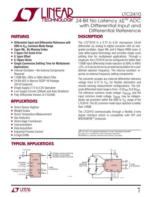
FEATURES■■■■■■■■■■■■■■■■■■■■■<strong>Differential</strong> <strong>Input</strong> <strong>and</strong> <strong>Differential</strong> Reference <strong>with</strong>GND to V CC Common Mode Range2ppm INL, <strong>No</strong> Missing Codes2.5ppm Full-Scale Error0.1ppm Offset0.16ppm <strong>No</strong>iseSingle Conversion Settling Time for MultiplexedApplicationsInternal Oscillator—<strong>No</strong> External ComponentsRequired110dB Min, 50Hz or 60Hz <strong>No</strong>tch Filter<strong>24</strong>-<strong>Bit</strong> <strong>ADC</strong> in Narrow SSOP-16 Package(SO-8 Footprint)Single Supply 2.7V to 5.5V OperationLow Supply Current (200µA) <strong>and</strong> Auto ShutdownFully <strong>Differential</strong> Version of LTC<strong>24</strong>00APPLICATIO SUDirect Sensor DigitizerWeight ScalesDirect Temperature MeasurementGas AnalyzersStrain-Gage TransducersInstrumentationData AcquisitionIndustrial Process Control6-Digit DVMs<strong>LTC<strong>24</strong>10</strong><strong>24</strong>-<strong>Bit</strong> <strong>No</strong> <strong>Latency</strong> ∆Σ TM <strong>ADC</strong><strong>with</strong> <strong>Differential</strong> <strong>Input</strong> <strong>and</strong><strong>Differential</strong> ReferenceDESCRIPTIOUThe LTC ® <strong>24</strong>10 is a 2.7V to 5.5V micropower <strong>24</strong>-bitdifferential ∆Σ analog to digital converter <strong>with</strong> an integratedoscillator, 2ppm INL <strong>and</strong> 0.16ppm RMS noise. Ituses delta-sigma technology <strong>and</strong> provides single cyclesettling time for multiplexed applications. Through asingle pin, the <strong>LTC<strong>24</strong>10</strong> can be configured for better than110dB input differential mode rejection at 50Hz or 60Hz±2%, or it can be driven by an external oscillator for a userdefined rejection frequency. The internal oscillator requiresno external frequency setting components.The converter accepts any external differential referencevoltage from 0.1V to V CC for flexible ratiometric <strong>and</strong>remote sensing measurement configurations. The fullscaledifferential input range is from –0.5V REF to 0.5V REF .The reference common mode voltage, V REFCM , <strong>and</strong> theinput common mode voltage, V INCM , may be independentlyset anywhere <strong>with</strong>in the GND to V CC range of the<strong>LTC<strong>24</strong>10</strong>. The DC common mode input rejection is betterthan 140dB.The <strong>LTC<strong>24</strong>10</strong> communicates through a flexible 3-wiredigital interface which is compatible <strong>with</strong> SPI <strong>and</strong>MICROWIRE TM protocols., LTC <strong>and</strong> LT are registered trademarks of Linear Technology Corporation.<strong>No</strong> <strong>Latency</strong> ∆Σ is a trademark of Linear Technology Corporation.MICROWIRE is a trademark of National Semiconductor Corporation.TYPICAL APPLICATIO SUREFERENCEVOLTAGE0.1V TO V CCANALOG INPUT RANGE–0.5V REF TO 0.5V REF2.7V TO 5.5V1µF2V CC F O1434561, 7, 8, 9, 10, 15, 16REF +REF –IN +IN –GND<strong>LTC<strong>24</strong>10</strong>SCKSDOCS131211V CC= INTERNAL OSC/50Hz REJECTION= EXTERNAL CLOCK SOURCE= INTERNAL OSC/60Hz REJECTION3-WIRESPI INTERFACE<strong>24</strong>10 TA01BRIDGEIMPEDANCE100Ω TO 10kV CC1µF23REF + V CC5IN +6<strong>LTC<strong>24</strong>10</strong>IN –4 REF – GND F O1, 7, 89, 10,15, 1614121311<strong>24</strong>10 TA02SDOSCKCS3-WIRESPI INTERFACE1
<strong>LTC<strong>24</strong>10</strong>ABSOLUTE AXI U RATI GSW W W(<strong>No</strong>tes 1, 2)Supply Voltage (V CC ) to GND.......................–0.3V to 7VAnalog <strong>Input</strong> Pins Voltageto GND .................................... –0.3V to (V CC + 0.3V)Reference <strong>Input</strong> Pins Voltageto GND .................................... –0.3V to (V CC + 0.3V)Digital <strong>Input</strong> Voltage to GND ........ –0.3V to (V CC + 0.3V)Digital Output Voltage to GND ..... –0.3V to (V CC + 0.3V)Operating Temperature Range<strong>LTC<strong>24</strong>10</strong>C ............................................... 0°C to 70°C<strong>LTC<strong>24</strong>10</strong>I............................................ –40°C to 85°CStorage Temperature Range ................. –65°C to 150°CLead Temperature (Soldering, 10 sec).................. 300°CUU U WPACKAGE/ORDER I FOR ATIOGNDV CCREF +REF –IN +IN –GNDGND12345678TOP VIEW161514131211109GN PACKAGE16-LEAD PLASTIC SSOPT JMAX = 125°C, θ JA = 110°C/WGNDGNDF OSCKSDOCSGNDGNDORDER PART NUMBER<strong>LTC<strong>24</strong>10</strong>CGN<strong>LTC<strong>24</strong>10</strong>IGNGN PART MARKING<strong>24</strong>10<strong>24</strong>10IConsult factory for parts specified <strong>with</strong> wider operating temperature ranges.ELECTRICAL CHARACTERISTICSThe ● denotes specifications which apply over the full operatingtemperature range, otherwise specifications are at T A = 25°C. (<strong>No</strong>tes 3, 4)PARAMETER CONDITIONS MIN TYP MAX UNITSResolution (<strong>No</strong> Missing Codes) 0.1V ≤ V REF ≤ V CC , –0.5 • V REF ≤ V IN ≤ 0.5 • V REF , (<strong>No</strong>te 5) ● <strong>24</strong> <strong>Bit</strong>sIntegral <strong>No</strong>nlinearity 5V ≤ V CC ≤ 5.5V, REF + = 2.5V, REF – = GND, V INCM = 1.25V, (<strong>No</strong>te 6) 1 ppm of V REF5V ≤ V CC ≤ 5.5V, REF + = 5V, REF – = GND, V INCM = 2.5V, (<strong>No</strong>te 6) ● 2 14 ppm of V REFREF + = 2.5V, REF – = GND, V INCM = 1.25V, (<strong>No</strong>te 6) 5 ppm of V REFOffset Error 2.5V ≤ REF + ≤ V CC , REF – = GND, ● 0.5 2.5 µVGND ≤ IN + = IN – ≤ V CC , (<strong>No</strong>te 14)Offset Error Drift 2.5V ≤ REF + ≤ V CC , REF – = GND, 10 nV/°CGND ≤ IN + = IN – ≤ V CCPositive Full-Scale Error 2.5V ≤ REF + ≤ V CC , REF – = GND, ● 2.5 12 ppm of V REFIN + = 0.75REF + , IN – = 0.25 • REF +Positive Full-Scale Error Drift 2.5V ≤ REF + ≤ V CC , REF – = GND, 0.03 ppm of V REF /°CIN + = 0.75REF + , IN – = 0.25 • REF +Negative Full-Scale Error 2.5V ≤ REF + ≤ V CC , REF – = GND, ● 2.5 12 ppm of V REFIN + = 0.25 • REF + , IN – = 0.75 • REF +Negative Full-Scale Error Drift 2.5V ≤ REF + ≤ V CC , REF – = GND, 0.03 ppm of V REF /°CIN + = 0.25 • REF + , IN – = 0.75 • REF +Total Unadjusted Error 5V ≤ V CC ≤ 5.5V, REF + = 2.5V, REF – = GND, V INCM = 1.25V 3 ppm of V REF5V ≤ V CC ≤ 5.5V, REF + = 5V, REF – = GND, V INCM = 2.5V 3 ppm of V REFREF + = 2.5V, REF – = GND, V INCM = 1.25V, (<strong>No</strong>te 6) 4 ppm of V REFOutput <strong>No</strong>ise 5V ≤ V CC ≤ 5.5V, REF + = 5V, REF – = GND, 0.8 µV RMSGND ≤ IN – = IN + ≤ V CC , (<strong>No</strong>te 13)2
CO VERTER CHARACTERISTICSUThe ● denotes specifications which apply over the full operatingtemperature range, otherwise specifications are at T A = 25°C. (<strong>No</strong>tes 3, 4)<strong>LTC<strong>24</strong>10</strong>PARAMETER CONDITIONS MIN TYP MAX UNITS<strong>Input</strong> Common Mode Rejection DC 2.5V ≤ REF + ≤ V CC , REF – = GND, ● 130 140 dBGND ≤ IN – = IN + ≤ V CC<strong>Input</strong> Common Mode Rejection 2.5V ≤ REF + ≤ V CC , REF – = GND, ● 140 dB60Hz ±2% GND ≤ IN – = IN + ≤ V CC , (<strong>No</strong>te 7)<strong>Input</strong> Common Mode Rejection 2.5V ≤ REF + ≤ V CC , REF – = GND, ● 140 dB50Hz ±2% GND ≤ IN – = IN + ≤ V CC , (<strong>No</strong>te 8)<strong>Input</strong> <strong>No</strong>rmal Mode Rejection (<strong>No</strong>te 7) ● 110 140 dB60Hz ±2%<strong>Input</strong> <strong>No</strong>rmal Mode Rejection (<strong>No</strong>te 8) ● 110 140 dB50Hz ±2%Reference Common Mode 2.5V ≤ REF + ≤ V CC , GND ≤ REF – ≤ 2.5V, ● 130 140 dBRejection DCV REF = 2.5V, IN – = IN + = GNDPower Supply Rejection, DC REF + = 2.5V, REF – = GND, IN – = IN + = GND 120 dBPower Supply Rejection, 60Hz ±2% REF + = 2.5V, REF – = GND, IN – = IN + = GND, (<strong>No</strong>te 7) 120 dBPower Supply Rejection, 50Hz ±2% REF + = 2.5V, REF – = GND, IN – = IN + = GND, (<strong>No</strong>te 8) 120 dBUU UUA ALOG I PUT A D REFERE CEThe ● denotes specifications which apply over the full operatingtemperature range, otherwise specifications are at T A = 25°C. (<strong>No</strong>te 3)SYMBOL PARAMETER CONDITIONS MIN TYP MAX UNITSIN + Absolute/Common Mode IN + Voltage ● GND – 0.3V V CC + 0.3V VIN – Absolute/Common Mode IN – Voltage ● GND – 0.3V V CC + 0.3V VV IN <strong>Input</strong> <strong>Differential</strong> Voltage Range ● –V REF /2 V REF /2 V(IN + – IN – )REF + Absolute/Common Mode REF + Voltage ● 0.1 V CC VREF – Absolute/Common Mode REF – Voltage ● GND V CC – 0.1V VV REF Reference <strong>Differential</strong> Voltage Range ● 0.1 V CC V(REF + – REF – )C S (IN + ) IN + Sampling Capacitance 18 pFC S (IN – ) IN – Sampling Capacitance 18 pFC S (REF + ) REF + Sampling Capacitance 18 pFC S (REF – ) REF – Sampling Capacitance 18 pFI DC_LEAK (IN + ) IN + DC Leakage Current CS = V CC , IN + = GND ● –10 1 10 nAI DC_LEAK (IN – ) IN – DC Leakage Current CS = V CC , IN – = GND ● –10 1 10 nAI DC_LEAK (REF + ) REF + DC Leakage Current CS = V CC , REF + = 5V ● –10 1 10 nAI DC_LEAK (REF – ) REF – DC Leakage Current CS = V CC , REF – = GND ● –10 1 10 nA3
<strong>LTC<strong>24</strong>10</strong>DIGITAL I PUTS A D DIGITAL OUTPUTSU UThe ● denotes specifications which apply over the fulloperating temperature range, otherwise specifications are at T A = 25°C. (<strong>No</strong>te 3)SYMBOL PARAMETER CONDITIONS MIN TYP MAX UNITSV IH High Level <strong>Input</strong> Voltage 2.7V ≤ V CC ≤ 5.5V ● 2.5 VCS, F O 2.7V ≤ V CC ≤ 3.3V 2.0 VV IL Low Level <strong>Input</strong> Voltage 4.5V ≤ V CC ≤ 5.5V ● 0.8 VCS, F O 2.7V ≤ V CC ≤ 5.5V 0.6 VV IH High Level <strong>Input</strong> Voltage 2.7V ≤ V CC ≤ 5.5V (<strong>No</strong>te 9) ● 2.5 VSCK 2.7V ≤ V CC ≤ 3.3V (<strong>No</strong>te 9) 2.0 VV IL Low Level <strong>Input</strong> Voltage 4.5V ≤ V CC ≤ 5.5V (<strong>No</strong>te 9) ● 0.8 VSCK 2.7V ≤ V CC ≤ 5.5V (<strong>No</strong>te 9) 0.6 VI IN Digital <strong>Input</strong> Current 0V ≤ V IN ≤ V CC ● –10 10 µACS, F OI IN Digital <strong>Input</strong> Current 0V ≤ V IN ≤ V CC (<strong>No</strong>te 9) ● –10 10 µASCKC IN Digital <strong>Input</strong> Capacitance 10 pFCS, F OC IN Digital <strong>Input</strong> Capacitance (<strong>No</strong>te 9) 10 pFSCKV OH High Level Output Voltage I O = –800µA ● V CC – 0.5V VSDOV OL Low Level Output Voltage I O = 1.6mA ● 0.4V VSDOV OH High Level Output Voltage I O = –800µA (<strong>No</strong>te 10) ● V CC – 0.5V VSCKV OL Low Level Output Voltage I O = 1.6mA (<strong>No</strong>te 10) ● 0.4V VSCKI OZ Hi-Z Output Leakage ● –10 10 µASDOPOWER REQUIRE E TSThe ● denotes specifications which apply over the full operating temperature range,otherwise specifications are at T A = 25°C. (<strong>No</strong>te 3)SYMBOL PARAMETER CONDITIONS MIN TYP MAX UNITSV CC Supply Voltage ● 2.7 5.5 VI CCWUSupply CurrentConversion Mode CS = 0V (<strong>No</strong>te 12) ● 200 300 µASleep Mode CS = V CC (<strong>No</strong>te 12) ● 20 30 µA4
TII G CHARACTERISTICSU W<strong>LTC<strong>24</strong>10</strong>The ● denotes specifications which apply over the full operating temperaturerange, otherwise specifications are at T A = 25°C. (<strong>No</strong>te 3)SYMBOL PARAMETER CONDITIONS MIN TYP MAX UNITSf EOSC External Oscillator Frequency Range ● 2.56 2000 kHzt HEO External Oscillator High Period ● 0.25 390 µst LEO External Oscillator Low Period ● 0.25 390 µst CONV Conversion Time F O = 0V ● 130.86 133.53 136.20 msF O = V CC ● 157.03 160.23 163.44 msExternal Oscillator (<strong>No</strong>te 11) ● 20510/f EOSC (in kHz) msf ISCK Internal SCK Frequency Internal Oscillator (<strong>No</strong>te 10) 19.2 kHzExternal Oscillator (<strong>No</strong>tes 10, 11) f EOSC /8 kHzD ISCK Internal SCK Duty Cycle (<strong>No</strong>te 10) ● 45 55 %f ESCK External SCK Frequency Range (<strong>No</strong>te 9) ● 2000 kHzt LESCK External SCK Low Period (<strong>No</strong>te 9) ● 250 nst HESCK External SCK High Period (<strong>No</strong>te 9) ● 250 nst DOUT_ISCK Internal SCK 32-<strong>Bit</strong> Data Output Time Internal Oscillator (<strong>No</strong>tes 10, 12) ● 1.64 1.67 1.70 msExternal Oscillator (<strong>No</strong>tes 10, 11) ● 256/f EOSC (in kHz) mst DOUT_ESCK External SCK 32-<strong>Bit</strong> Data Output Time (<strong>No</strong>te 9) ● 32/f ESCK (in kHz) mst 1 CS ↓ to SDO Low Z ● 0 200 nst2 CS ↑ to SDO High Z ● 0 200 nst3 CS ↓ to SCK ↓ (<strong>No</strong>te 10) ● 0 200 nst4 CS ↓ to SCK ↑ (<strong>No</strong>te 9) ● 50 nst KQMAX SCK ↓ to SDO Valid ● 220 nst KQMIN SDO Hold After SCK ↓ (<strong>No</strong>te 5) ● 15 nst 5 SCK Set-Up Before CS ↓ ● 50 nst 6 SCK Hold After CS ↓ ● 50 ns<strong>No</strong>te 1: Absolute Maximum Ratings are those values beyond which thelife of the device may be impaired.<strong>No</strong>te 2: All voltage values are <strong>with</strong> respect to GND.<strong>No</strong>te 3: V CC = 2.7 to 5.5V unless otherwise specified.V REF = REF + – REF – , V REFCM = (REF + + REF – )/2;V IN = IN + – IN – , V INCM = (IN + + IN – )/2.<strong>No</strong>te 4: F O pin tied to GND or to V CC or to external conversion clocksource <strong>with</strong> f EOSC = 153600Hz unless otherwise specified.<strong>No</strong>te 5: Guaranteed by design, not subject to test.<strong>No</strong>te 6: Integral nonlinearity is defined as the deviation of a code froma straight line passing through the actual endpoints of the transfercurve. The deviation is measured from the center of the quantizationb<strong>and</strong>.<strong>No</strong>te 7: F O = 0V (internal oscillator) or f EOSC = 153600Hz ±2%(external oscillator).<strong>No</strong>te 8: F O = V CC (internal oscillator) or f EOSC = 128000Hz ±2%(external oscillator).<strong>No</strong>te 9: The converter is in external SCK mode of operation such thatthe SCK pin is used as digital input. The frequency of the clock signaldriving SCK during the data output is f ESCK <strong>and</strong> is expressed in kHz.<strong>No</strong>te 10: The converter is in internal SCK mode of operation such thatthe SCK pin is used as digital output. In this mode of operation theSCK pin has a total equivalent load capacitance C LOAD = 20pF.<strong>No</strong>te 11: The external oscillator is connected to the F O pin. The externaloscillator frequency, f EOSC , is expressed in kHz.<strong>No</strong>te 12: The converter uses the internal oscillator.F O = 0V or F O = V CC .<strong>No</strong>te 13: The output noise includes the contribution of the internalcalibration operations.<strong>No</strong>te 14: Guaranteed by design <strong>and</strong> test correlation.5
<strong>LTC<strong>24</strong>10</strong>TYPICAL PERFOR A CE CHARACTERISTICSU WRMS <strong>No</strong>ise vs Temperature (T A )RMS <strong>No</strong>ise vs V CCRMS NOISE (nV)850825800775750725V CC = 5VREF + = 5VREF – = GNDV REF = 5VIN + = V INCMRMS NOISE (nV)850825800775750725V CC = 5VREF + = 5VREF – = GNDIN + = 2.5VIN – = 2.5VV IN = 0VF O = GNDRMS NOISE (nV)850825800775750725REF + = 2.5VREF – = GNDV REF = 2.5VIN + = GNDIN – = GNDF O = GNDT A = 25°C700675IN – = V INCMV IN = 0VF O = GNDT A = 25°C700675700675650–0.5 0 0.5 1 1.5 2 2.5 3 3.5 4 4.5 5 5.5V INCM (V)RMS <strong>No</strong>ise vs V INCMOffset Error vs Temperature (T A )650–50 –25 0 25 50 75 100TEMPERATURE (°C)6502.7 3.1 3.5 3.9 4.3 4.7 5.1 5.5V CC (V)<strong>24</strong>10 G19<strong>24</strong>10 G20<strong>24</strong>10 G21RMS <strong>No</strong>ise vs V REFOffset Error vs V INCMRMS NOISE (nV)850825800775750725700675V CC = 5VREF – = GNDIN + = GNDIN – = GNDF O = GNDT A = 25°COFFSET ERROR (ppm OF V REF )0.30.20.10–0.1–0.2V CC = 5VREF + = 5VREF – = GNDV REF = 5VIN + = V INCMIN – = V INCMV IN = 0VF O = GNDT A = 25°COFFSET ERROR (ppm OF V REF )0.30.20.10–0.1–0.2V CC = 5VREF + = 5VREF – = GNDIN + = 2.5VIN – = 2.5VV IN = 0VF O = GND6500 0.5 1 1.5 2 2.5 3 3.5 4 4.5 5V REF (V)–0.3–0.5 0 0.5 1 1.5 2 2.5 3 3.5 4 4.5 5 5.5V INCM (V)–0.3–50 –25 0 25 50 75 100TEMPERATURE (°C)<strong>24</strong>10 G22<strong>24</strong>10 G23<strong>24</strong>10 G<strong>24</strong>Offset Error vs V CCOffset Error vs V REF+Full-Scale Error vsTemperature (T A )0.30.33OFFSET ERROR (ppm OF V REF )0.20.10–0.1–0.2REF + = 2.5VREF – = GNDV REF = 2.5VIN + = GNDIN – = GNDF O = GNDT A = 25°COFFSET ERROR (ppm OF V REF )0.20.10–0.1–0.2V CC = 5VREF – = GNDIN + = GNDIN – = GNDF O = GNDT A = 25°C+FULL-SCALE ERROR (ppm OF V REF )210–1–2V CC = 5VREF + = 5VREF – = GNDIN + = 2.5VIN – = GNDF O = GND–0.32.7 3.1 3.5 3.9 4.3 4.7 5.1 5.5V CC (V)–0.30 0.5 1 1.5 2 2.5 3 3.5 4 4.5 5V REF (V)–3–45 –30 –15 0 15 30 45 60 75 90TEMPERATURE (°C)<strong>24</strong>10 G25<strong>24</strong>10 G26<strong>24</strong>10 G278
<strong>LTC<strong>24</strong>10</strong>TYPICAL PERFOR A CE CHARACTERISTICSU W+Full-Scale Error vs V CC+Full-Scale Error vs V REF– Full-Scale Error vsTemperature (T A )+FULL-SCALE ERROR (ppm OF V REF )3210–1–2REF + = 2.5VREF – = GNDV REF = 2.5VIN + = 1.25VIN – = GNDF O = GNDT A = 25°C–32.7 3.1 3.5 3.9 4.3 4.7 5.1 5.5V CC (V)+FULL-SCALE ERROR (ppm OF V REF )3210V CC = 5VREF + = V REF–1REF – = GNDIN + = 0.5 • REF +IN – = GND–2F O = GNDT A = 25°C–30 0.5 1 1.5 2 2.5 3 3.5 4 4.5 5V REF (V)–FULL-SCALE ERROR (ppm OF V REF )3210–1–2V CC = 5VREF + = 5VREF – = GNDIN + = GNDIN – = 2.5VF O = GND–3–45 –30 –15 0 15 30 45 60 75 90TEMPERATURE (°C)<strong>24</strong>10 G28<strong>24</strong>10 G29<strong>24</strong>10 G30–Full-Scale Error vs V CC–Full-Scale Error vs V REFPSRR vs Frequency at V CC–FULL-SCALE ERROR (ppm OF V REF )3210–1–2REF + = 2.5VREF – = GNDV REF = 2.5VIN + = GNDIN – = 1.25VF O = GNDT A = 25°C–FULL-SCALE ERROR (ppm OF V REF )3210–1–2V CC = 5VREF + = V REFREF – = GNDIN + = GNDIN – = 0.5 • REF +F O = GNDT A = 25°CREJECTION (dB)0–20–40–60–80–100–120V CC = 4.1V DC ± 1.4VREF + = 2.5VREF – = GNDIN + = GNDIN – = GNDF O = GNDT A = 25°C–32.7 3.1 3.5 3.9 4.3 4.7 5.1 5.5V CC (V)<strong>24</strong>10 G31–30 0.5 1 1.5 2 2.5 3 3.5 4 4.5 5V REF (V)<strong>24</strong>10 G32–1400.01 0.1 1 10 100FREQUENCY AT V CC (Hz)<strong>24</strong>10 G33PSRR vs Frequency at V CCPSRR vs Frequency at V CCPSRR vs Frequency at V CCREJECTION (dB)0–20–40–60–80–100–120V CC = 4.1V DC ± 1.4VREF + = 2.5VREF – = GNDIN + = GNDIN – = GNDF O = GNDT A = 25°CREJECTION (dB)0–20–40–60–80–100–120REF + = 2.5VREF – = GNDIN + = GNDIN – = GNDF O = GNDT A = 25°CREJECTION (dB)0–10–20–30–40–50–60–70–80–90V CC = 4.1V DC ± 0.7VREF + = 2.5VREF – = GNDIN + = GNDIN – = GNDF O = GNDT A = 25°C–1400 30 60 90 120 150 180 210 <strong>24</strong>0FREQUENCY AT V CC (Hz)<strong>24</strong>10 G34–1401 10 100 1k 10k 100k 1MFREQUENCY AT V CC (Hz)<strong>24</strong>10 G35–1007600 7620 7640 7660 7680 7700 7720 7740FREQUENCY AT V CC (Hz)<strong>24</strong>10 G369
<strong>LTC<strong>24</strong>10</strong>TYPICAL PERFOR A CE CHARACTERISTICSSUPPLY CURRENT (µA)220210200190180170Conversion Current vsTemperature (T A )F O = GNDCS = GNDSCK = NCSDO = NC V CC = 5.5VV CC = 4.1VV CC = 2.7VU W160–45 –30 –15 0 15 30 45 60 75 90TEMPERATURE (°C)<strong>24</strong>10 G37SUPPLY CURRENT (µA)11001000900800700600500400300200Conversion Current vsOutput Data RateV CC = 5VREF + = 5VREF – = GNDIN + = GNDIN – = GNDT A = 25°CF O = EXTERNAL OSCCS = GNDSCK = NCSDO = NC1000 10 20 30 40 50 60 70 80 90 100OUTPUT DATA RATE (READINGS/SEC) <strong>24</strong>10 G38SUPPLY CURRENT (µA)23222120191817Sleep Current vs Temperature (T A )F O = GNDCS = V CCSCK = NCSDO = NCV CC = 4.1VV CC = 5.5VV CC = 2.7V16–45 –30 –15 0 15 30 45 60 75 90TEMPERATURE (°C)<strong>24</strong>10 G39PI FU CTIO SU U UGND (Pins 1, 7, 8, 9, 10, 15, 16): Ground. Multiple groundpins internally connected for optimum ground current flow<strong>and</strong> V CC decoupling. Connect each one of these pins to aground plane through a low impedance connection. All sevenpins must be connected to ground for proper operation.V CC (Pin 2): Positive Supply Voltage. Bypass to GND(Pin␣ 1) <strong>with</strong> a 10µF tantalum capacitor in parallel <strong>with</strong>0.1µF ceramic capacitor as close to the part as possible.REF + (Pin 3), REF – (Pin 4): <strong>Differential</strong> Reference <strong>Input</strong>.The voltage on these pins can have any value between GND<strong>and</strong> V CC as long as the reference positive input, REF + , ismaintained more positive than the reference negativeinput, REF – , by at least 0.1V.IN + (Pin 5), IN – (Pin 6): <strong>Differential</strong> Analog <strong>Input</strong>. Thevoltage on these pins can have any value betweenGND – 0.3V <strong>and</strong> V CC + 0.3V. Within these limits theconverter bipolar input range (V IN = IN + – IN – ) extendsfrom –0.5 • (V REF ) to 0.5 • (V REF ). Outside this input rangethe converter produces unique overrange <strong>and</strong> underrangeoutput codes.CS (Pin 11): Active LOW Digital <strong>Input</strong>. A LOW on this pinenables the SDO digital output <strong>and</strong> wakes up the <strong>ADC</strong>.Following each conversion the <strong>ADC</strong> automatically entersthe Sleep mode <strong>and</strong> remains in this low power state aslong as CS is HIGH. A LOW-to-HIGH transition on CSduring the Data Output transfer aborts the data transfer<strong>and</strong> starts a new conversion.10SDO (Pin 12): Three-State Digital Output. During the DataOutput period, this pin is used as serial data output. Whenthe chip select CS is HIGH (CS = V CC ) the SDO pin is in ahigh impedance state. During the Conversion <strong>and</strong> Sleepperiods, this pin is used as the conversion status output.The conversion status can be observed by pulling CS LOW.SCK (Pin 13): Bidirectional Digital Clock Pin. In InternalSerial Clock Operation mode, SCK is used as digital outputfor the internal serial interface clock during the DataOutput period. In External Serial Clock Operation mode,SCK is used as digital input for the external serial interfaceclock during the Data Output period. A weak internal pullupis automatically activated in Internal Serial Clock Operationmode. The Serial Clock Operation mode is determinedby the logic level applied to the SCK pin at power upor during the most recent falling edge of CS.F O (Pin 14): Frequency Control Pin. Digital input thatcontrols the <strong>ADC</strong>’s notch frequencies <strong>and</strong> conversiontime. When the F O pin is connected to V CC (F O = V CC ), theconverter uses its internal oscillator <strong>and</strong> the digital filterfirst null is located at 50Hz. When the F O pin is connectedto GND (F O = OV), the converter uses its internal oscillator<strong>and</strong> the digital filter first null is located at 60Hz. When F Ois driven by an external clock signal <strong>with</strong> a frequency f EOSC ,the converter uses this signal as its system clock <strong>and</strong> thedigital filter first null is located at a frequency f EOSC /2560.
<strong>LTC<strong>24</strong>10</strong>WFU CTIO AL BLOCK DIAGRAV CCU UINTERNALOSCILLATORGNDAUTOCALIBRATIONAND CONTROLF O(INT/EXT)IN +IN –+–∫∫∫∑<strong>ADC</strong>SERIALINTERFACESDOSCKREF +REF –DECIMATING FIRCS– +DACFigure 1. Functional Block Diagram<strong>24</strong>10 FDTEST CIRCUITSV CCSDO1.69kC LOAD = 20pFSDO1.69kC LOAD = 20pFHi-Z TO V OHV OL TO V OHV OH TO Hi-Z<strong>24</strong>10 TA03Hi-Z TO V OLV OH TO V OLV OL TO Hi-Z<strong>24</strong>10 TA04APPLICATIO S I FORCONVERTER OPERATIONATIOU W U UConverter Operation CycleThe <strong>LTC<strong>24</strong>10</strong> is a low power, delta-sigma analog-todigitalconverter <strong>with</strong> an easy to use 3-wire serial interface(see Figure 1). Its operation is made up of three states. Theconverter operating cycle begins <strong>with</strong> the conversion,followed by the low power sleep state <strong>and</strong> ends <strong>with</strong> thedata output (see Figure 2). The 3-wire interface consistsof serial data output (SDO), serial clock (SCK) <strong>and</strong> chipselect (CS).Initially, the <strong>LTC<strong>24</strong>10</strong> performs a conversion. Once theconversion is complete, the device enters the sleep state.While in this sleep state, power consumption is reduced byan order of magnitude. The part remains in the sleep stateas long as CS is HIGH. The conversion result is heldindefinitely in a static shift register while the converter isin the sleep state.FALSECONVERTSLEEPCS = LOWANDSCKTRUEDATA OUTPUT<strong>24</strong>10 F02Figure 2. <strong>LTC<strong>24</strong>10</strong> State Transition Diagram11
<strong>LTC<strong>24</strong>10</strong>APPLICATIO S I FOROnce CS is pulled LOW, the device begins outputting theconversion result. There is no latency in the conversionresult. The data output corresponds to the conversion justperformed. This result is shifted out on the serial data outpin (SDO) under the control of the serial clock (SCK). Datais updated on the falling edge of SCK allowing the user toreliably latch data on the rising edge of SCK (see Figure 3).The data output state is concluded once 32 bits are readout of the <strong>ADC</strong> or when CS is brought HIGH. The deviceautomatically initiates a new conversion <strong>and</strong> the cyclerepeats.Through timing control of the CS <strong>and</strong> SCK pins, the<strong>LTC<strong>24</strong>10</strong> offers several flexible modes of operation(internal or external SCK <strong>and</strong> free-running conversionmodes). These various modes do not require programmingconfiguration registers; moreover, they do not disturbthe cyclic operation described above. These modes ofoperation are described in detail in the Serial InterfaceTiming Modes section.Conversion ClockA major advantage the delta-sigma converter offers overconventional type converters is an on-chip digital filter(commonly implemented as a Sinc or Comb filter). Forhigh resolution, low frequency applications, this filter istypically designed to reject line frequencies of 50 or 60Hzplus their harmonics. The filter rejection performance isdirectly related to the accuracy of the converter systemclock. The <strong>LTC<strong>24</strong>10</strong> incorporates a highly accurate onchiposcillator. This eliminates the need for external frequencysetting components such as crystals or oscillators.Clocked by the on-chip oscillator, the <strong>LTC<strong>24</strong>10</strong>achieves a minimum of 110dB rejection at the line frequency(50Hz or 60Hz ±2%).Ease of UseThe <strong>LTC<strong>24</strong>10</strong> data output has no latency, filter settlingdelay or redundant data associated <strong>with</strong> the conversioncycle. There is a one-to-one correspondence between theconversion <strong>and</strong> the output data. Therefore, multiplexingmultiple analog voltages is easy.12ATIOU W U UThe <strong>LTC<strong>24</strong>10</strong> performs offset <strong>and</strong> full-scale calibrationsevery conversion cycle. This calibration is transparent tothe user <strong>and</strong> has no effect on the cyclic operation describedabove. The advantage of continuous calibration isextreme stability of offset <strong>and</strong> full-scale readings <strong>with</strong> respectto time, supply voltage change <strong>and</strong> temperature drift.Power-Up SequenceThe <strong>LTC<strong>24</strong>10</strong> automatically enters an internal reset statewhen the power supply voltage V CC drops below approximately2.2V. This feature guarantees the integrity of theconversion result <strong>and</strong> of the serial interface mode selection.(See the 2-wire I/O sections in the Serial InterfaceTiming Modes section.)When the V CC voltage rises above this critical threshold,the converter creates an internal power-on-reset (POR)signal <strong>with</strong> a duration of approximately 0.5ms. The PORsignal clears all internal registers. Following the PORsignal, the <strong>LTC<strong>24</strong>10</strong> starts a normal conversion cycle <strong>and</strong>follows the succession of states described above. The firstconversion result following POR is accurate <strong>with</strong>in thespecifications of the device if the power supply voltage isrestored <strong>with</strong>in the operating range (2.7V to 5.5V) beforethe end of the POR time interval.Reference Voltage RangeThis converter accepts a truly differential external referencevoltage. The absolute/common mode voltage specificationfor the REF + <strong>and</strong> REF – pins covers the entire rangefrom GND to V CC . For correct converter operation, theREF + pin must always be more positive than the REF – pin.The <strong>LTC<strong>24</strong>10</strong> can accept a differential reference voltagefrom 0.1V to V CC . The converter output noise is determinedby the thermal noise of the front-end circuits, <strong>and</strong>as such, its value in nanovolts is nearly constant <strong>with</strong>reference voltage. A decrease in reference voltage will notsignificantly improve the converter’s effective resolution.On the other h<strong>and</strong>, a reduced reference voltage will improvethe converter’s overall INL performance. A reducedreference voltage will also improve the converter performancewhen operated <strong>with</strong> an external conversion clock(external F O signal) at substantially higher output datarates (see the Output Data Rate section).
<strong>LTC<strong>24</strong>10</strong>APPLICATIO S I FORATIOU W U U<strong>Input</strong> Voltage RangeThe analog input is truly differential <strong>with</strong> an absolute/common mode range for the IN + <strong>and</strong> IN – input pinsextending from GND – 0.3V to V CC + 0.3V. Outsidethese limits, the ESD protection devices begin to turn on<strong>and</strong> the errors due to input leakage current increaserapidly. Within these limits, the <strong>LTC<strong>24</strong>10</strong> converts thebipolar differential input signal, V IN = IN + – IN – , from–FS = –0.5 • V REF to +FS = 0.5 • V REF where V REF =REF + – REF – . Outside this range, the converter indicatesthe overrange or the underrange condition using distinctoutput codes.<strong>Input</strong> signals applied to IN + <strong>and</strong> IN – pins may extend by300mV below ground <strong>and</strong> above V CC . In order to limit anyfault current, resistors of up to 5k may be added in series<strong>with</strong> the IN + <strong>and</strong> IN – pins <strong>with</strong>out affecting the performanceof the device. In the physical layout, it is importantto maintain the parasitic capacitance of the connectionbetween these series resistors <strong>and</strong> the corresponding pinsas low as possible; therefore, the resistors should belocated as close as practical to the pins. The effect of theseries resistance on the converter accuracy can be evaluatedfrom the curves presented in the <strong>Input</strong> Current/Reference Current sections. In addition, series resistorswill introduce a temperature dependent offset error due tothe input leakage current. A 1nA input leakage current willdevelop a 1ppm offset error on a 5k resistor if V REF = 5V.This error has a very strong temperature dependency.Output Data FormatThe <strong>LTC<strong>24</strong>10</strong> serial output data stream is 32 bits long. Thefirst 3 bits represent status information indicating the sign<strong>and</strong> conversion state. The next <strong>24</strong> bits are the conversionresult, MSB first. The remaining 5 bits are sub LSBsbeyond the <strong>24</strong>-bit level that may be included in averagingor discarded <strong>with</strong>out loss of resolution. The third <strong>and</strong>fourth bit together are also used to indicate an underrangecondition (the differential input voltage is below –FS) or anoverrange condition (the differential input voltage is above+FS).<strong>Bit</strong> 31 (first output bit) is the end of conversion (EOC)indicator. This bit is available at the SDO pin during theconversion <strong>and</strong> sleep states whenever the CS pin is LOW.This bit is HIGH during the conversion <strong>and</strong> goes LOWwhen the conversion is complete.<strong>Bit</strong> 30 (second output bit) is a dummy bit (DMY) <strong>and</strong> isalways LOW.<strong>Bit</strong> 29 (third output bit) is the conversion result sign indicator(SIG). If V IN is >0, this bit is HIGH. If V IN is
<strong>LTC<strong>24</strong>10</strong>APPLICATIO S I FORATIOU W U Uon the rising edge of the 32nd SCK pulse. On the fallingedge of the 32nd SCK pulse, SDO goes HIGH indicating theinitiation of a new conversion cycle. This bit serves as EOC(<strong>Bit</strong> 31) for the next conversion cycle. Table 2 summarizesthe output data format.As long as the voltage on the IN + <strong>and</strong> IN – pins is maintained<strong>with</strong>in the – 0.3V to (V CC + 0.3V) absolute maximumoperating range, a conversion result is generated for anydifferential input voltage V IN from –FS = –0.5 • V REF to+FS = 0.5 • V REF . For differential input voltages greater than+FS, the conversion result is clamped to the value correspondingto the +FS + 1LSB. For differential input voltagesbelow –FS, the conversion result is clamped to the valuecorresponding to –FS – 1LSB.Frequency Rejection Selection (F O )The <strong>LTC<strong>24</strong>10</strong> internal oscillator provides better than 110dBnormal mode rejection at the line frequency <strong>and</strong> all itsharmonics for 50Hz ±2% or 60Hz ±2%. For 60Hz rejection,F O should be connected to GND while for 50Hzrejection the F O pin should be connected to V CC .The selection of 50Hz or 60Hz rejection can also be madeby driving F O to an appropriate logic level. A selectionchange during the sleep or data output states will notdisturb the converter operation. If the selection is madeduring the conversion state, the result of the conversion inprogress may be outside specifications but the followingconversions will not be affected.When a fundamental rejection frequency different from50Hz or 60Hz is required or when the converter must beCSBIT 31BIT 30BIT 29BIT 28BIT 27 BIT 5BIT 0SDOHi-ZEOC“0”SIGMSBLSB <strong>24</strong>SCK1 2 3 4 5 26 27 32SLEEP DATA OUTPUT CONVERSIONFigure 3. Output Data Timing<strong>24</strong>10 F0314Table 2. <strong>LTC<strong>24</strong>10</strong> Output Data Format<strong>Differential</strong> <strong>Input</strong> Voltage <strong>Bit</strong> 31 <strong>Bit</strong> 30 <strong>Bit</strong> 29 <strong>Bit</strong> 28 <strong>Bit</strong> 27 <strong>Bit</strong> 26 <strong>Bit</strong> 25 … <strong>Bit</strong> 0V IN * EOC DMY SIG MSBV IN * ≥ 0.5 • V REF ** 0 0 1 1 0 0 0 … 00.5 • V REF ** – 1LSB 0 0 1 0 1 1 1 … 10.25 • V REF ** 0 0 1 0 1 0 0 … 00.25 • V REF ** – 1LSB 0 0 1 0 0 1 1 … 10 0 0 1 0 0 0 0 … 0–1LSB 0 0 0 1 1 1 1 … 1–0.25 • V REF ** 0 0 0 1 1 0 0 … 0–0.25 • V REF ** – 1LSB 0 0 0 1 0 1 1 … 1–0.5 • V REF ** 0 0 0 1 0 0 0 … 0V IN * < –0.5 • V REF ** 0 0 0 0 1 1 1 … 1*The differential input voltage V IN = IN + – IN – .**The differential reference voltage V REF = REF + – REF – .
<strong>LTC<strong>24</strong>10</strong>APPLICATIO S I FORATIOU W U Usynchronized <strong>with</strong> an outside source, the <strong>LTC<strong>24</strong>10</strong> canoperate <strong>with</strong> an external conversion clock. The converterautomatically detects the presence of an external clocksignal at the F O pin <strong>and</strong> turns off the internal oscillator. Thefrequency f EOSC of the external signal must be at least2560Hz (1Hz notch frequency) to be detected. The externalclock signal duty cycle is not significant as long as theminimum <strong>and</strong> maximum specifications for the high <strong>and</strong>low periods t HEO <strong>and</strong> t LEO are observed.While operating <strong>with</strong> an external conversion clock of afrequency f EOSC , the <strong>LTC<strong>24</strong>10</strong> provides better than 110dBnormal mode rejection in a frequency range f EOSC /2560±4% <strong>and</strong> its harmonics. The normal mode rejection as afunction of the input frequency deviation from f EOSC /2560is shown in Figure 4.Whenever an external clock is not present at the F O pin, theconverter automatically activates its internal oscillator <strong>and</strong>enters the Internal Conversion Clock mode. The <strong>LTC<strong>24</strong>10</strong>operation will not be disturbed if the change of conversionclock source occurs during the sleep state or during thedata output state while the converter uses an externalserial clock. If the change occurs during the conversionstate, the result of the conversion in progress may beoutside specifications but the following conversions willnot be affected. If the change occurs during the data outputstate <strong>and</strong> the converter is in the Internal SCK mode, theserial clock duty cycle may be affected but the serial datastream will remain valid.NORMAL MODE REJECTION (dB)–80–85–90–95–100–105–110–115–120–125–130–135–140–12 –8 –4 0 4 8 12DIFFERENTIAL INPUT SIGNAL FREQUENCYDEVIATION FROM NOTCH FREQUENCY f EOSC /2560(%)<strong>24</strong>10 F04Figure 4. <strong>LTC<strong>24</strong>10</strong> <strong>No</strong>rmal Mode Rejection WhenUsing an External Oscillator of Frequency f EOSCTable 3 summarizes the duration of each state <strong>and</strong> theachievable output data rate as a function of F O .SERIAL INTERFACE PINSThe <strong>LTC<strong>24</strong>10</strong> transmits the conversion results <strong>and</strong> receivesthe start of conversion comm<strong>and</strong> through a synchronous3-wire interface. During the conversion <strong>and</strong>sleep states, this interface can be used to assess theconverter status <strong>and</strong> during the data output state it is usedto read the conversion result.Table 3. <strong>LTC<strong>24</strong>10</strong> State DurationState Operating Mode DurationCONVERT Internal Oscillator F O = LOW 133ms, Output Data Rate ≤ 7.5 Readings/s(60Hz Rejection)F O = HIGH160ms, Output Data Rate ≤ 6.2 Readings/s(50Hz Rejection)External Oscillator F O = External Oscillator 20510/f EOSC s, Output Data Rate ≤ f EOSC /20510 Readings/s<strong>with</strong> Frequency f EOSC kHz(f EOSC /2560 Rejection)SLEEPAs Long As CS = HIGH Until CS = LOW <strong>and</strong> SCKDATA OUTPUT Internal Serial Clock F O = LOW/HIGH As Long As CS = LOW But <strong>No</strong>t Longer Than 1.67ms(Internal Oscillator)(32 SCK cycles)F O = External Oscillator <strong>with</strong> As Long As CS = LOW But <strong>No</strong>t Longer Than 256/f EOSC msFrequency f EOSC kHz(32 SCK cycles)External Serial Clock <strong>with</strong>As Long As CS = LOW But <strong>No</strong>t Longer Than 32/f SCK msFrequency f SCK kHz(32 SCK cycles)15
<strong>LTC<strong>24</strong>10</strong>APPLICATIO S I FORSerial Clock <strong>Input</strong>/Output (SCK)ATIOU W U UThe serial clock signal present on SCK (Pin 13) is used tosynchronize the data transfer. Each bit of data is shifted outthe SDO pin on the falling edge of the serial clock.In the Internal SCK mode of operation, the SCK pin is anoutput <strong>and</strong> the <strong>LTC<strong>24</strong>10</strong> creates its own serial clock bydividing the internal conversion clock by 8. In the ExternalSCK mode of operation, the SCK pin is used as input. Theinternal or external SCK mode is selected on power-up <strong>and</strong>then reselected every time a HIGH-to-LOW transition isdetected at the CS pin. If SCK is HIGH or floating at powerupor during this transition, the converter enters the internalSCK mode. If SCK is LOW at power-up or during thistransition, the converter enters the external SCK mode.Serial Data Output (SDO)The serial data output pin, SDO (Pin 12), provides theresult of the last conversion as a serial bit stream (MSBfirst) during the data output state. In addition, the SDO pinis used as an end of conversion indicator during theconversion <strong>and</strong> sleep states.When CS (Pin 11) is HIGH, the SDO driver is switched toa high impedance state. This allows sharing the serialinterface <strong>with</strong> other devices. If CS is LOW during theconvert or sleep state, SDO will output EOC. If CS is LOWduring the conversion phase, the EOC bit appears HIGH onthe SDO pin. Once the conversion is complete, EOC goesLOW. The device remains in the sleep state until the firstrising edge of SCK occurs while CS = LOW.Chip Select <strong>Input</strong> (CS)The active LOW chip select, CS (Pin 11), is used to test theconversion status <strong>and</strong> to enable the data output transfer asdescribed in the previous sections.In addition, the CS signal can be used to trigger a newconversion cycle before the entire serial data transfer hasbeen completed. The <strong>LTC<strong>24</strong>10</strong> will abort any serial datatransfer in progress <strong>and</strong> start a new conversion cycleanytime a LOW-to-HIGH transition is detected at the CSpin after the converter has entered the data output state(i.e., after the first rising edge of SCK occurs <strong>with</strong>CS␣=␣LOW).Finally, CS can be used to control the free-running modesof operation, see Serial Interface Timing Modes section.Grounding CS will force the <strong>ADC</strong> to continuously convertat the maximum output rate selected by F O . Tying acapacitor to CS will reduce the output rate <strong>and</strong> powerdissipation by a factor proportional to the capacitor’svalue, see Figures 12 to 14.SERIAL INTERFACE TIMING MODESThe <strong>LTC<strong>24</strong>10</strong>’s 3-wire interface is SPI <strong>and</strong> MICROWIREcompatible. This interface offers several flexible modes ofoperation. These include internal/external serial clock,2- or 3-wire I/O, single cycle conversion <strong>and</strong> autostart. Thefollowing sections describe each of these serial interfacetiming modes in detail. In all these cases, the convertercan use the internal oscillator (F O = LOW or F O = HIGH) oran external oscillator connected to the F O pin. Refer toTable␣ 4 for a summary.External Serial Clock, Single Cycle Operation(SPI/MICROWIRE Compatible)This timing mode uses an external serial clock to shift outthe conversion result <strong>and</strong> a CS signal to monitor <strong>and</strong>control the state of the conversion cycle, see Figure 5.Table 4. <strong>LTC<strong>24</strong>10</strong> Interface Timing ModesConversion Data ConnectionSCK Cycle Output <strong>and</strong>Configuration Source Control Control WaveformsExternal SCK, Single Cycle Conversion External CS <strong>and</strong> SCK CS <strong>and</strong> SCK Figures 5, 6External SCK, 2-Wire I/O External SCK SCK Figure 7Internal SCK, Single Cycle Conversion Internal CS ↓ CS ↓ Figures 8, 9Internal SCK, 2-Wire I/O, Continuous Conversion Internal Continuous Internal Figure 10Internal SCK, Autostart Conversion Internal C EXT Internal Figure 1116
<strong>LTC<strong>24</strong>10</strong>APPLICATIO S I FORATIOU W U UThe serial clock mode is selected on the falling edge of CS.To select the external serial clock mode, the serial clock pin(SCK) must be LOW during each CS falling edge.The serial data output pin (SDO) is Hi-Z as long as CS isHIGH. At any time during the conversion cycle, CS may bepulled LOW in order to monitor the state of the converter.While CS is pulled LOW, EOC is output to the SDO pin.EOC␣ =␣ 1 while a conversion is in progress <strong>and</strong> EOC = 0 ifthe device is in the sleep state. Independent of CS, thedevice automatically enters the low power sleep state oncethe conversion is complete.When the device is in the sleep state (EOC = 0), itsconversion result is held in an internal static shift register.The device remains in the sleep state until the firstrising edge of SCK is seen while CS is LOW. Data is shiftedout the SDO pin on each falling edge of SCK. This enablesexternal circuitry to latch the output on the rising edge ofSCK. EOC can be latched on the first rising edge of SCK<strong>and</strong> the last bit of the conversion result can be latched onthe 32nd rising edge of SCK. On the 32nd falling edge ofSCK, the device begins a new conversion. SDO goes HIGH(EOC = 1) indicating a conversion is in progress.At the conclusion of the data cycle, CS may remain LOW<strong>and</strong> EOC monitored as an end-of-conversion interrupt.Alternatively, CS may be driven HIGH setting SDO to Hi-Z.As described above, CS may be pulled LOW at any time inorder to monitor the conversion status.Typically, CS remains LOW during the data output state.However, the data output state may be aborted by pullingCS HIGH anytime between the first rising edge <strong>and</strong> the32nd falling edge of SCK, see Figure 6. On the rising edgeof CS, the device aborts the data output state <strong>and</strong> immediatelyinitiates a new conversion. This is useful for systemsnot requiring all 32 bits of output data, aborting aninvalid conversion cycle or synchronizing the start of aconversion.External Serial Clock, 2-Wire I/OThis timing mode utilizes a 2-wire serial I/O interface. Theconversion result is shifted out of the device by an externallygenerated serial clock (SCK) signal, see Figure 7. CSmay be permanently tied to ground, simplifying the userinterface or isolation barrier.The external serial clock mode is selected at the end of thepower-on reset (POR) cycle. The POR cycle is concludedapproximately 0.5ms after V CC exceeds 2.2V. The levelapplied to SCK at this time determines if SCK is internal orexternal. SCK must be driven LOW prior to the end of PORin order to enter the external serial clock timing mode.REFERENCEVOLTAGE0.1V TO V CCANALOG INPUT RANGE–0.5V REF TO 0.5V REF2.7V TO 5.5V1µF2V CC F O14<strong>LTC<strong>24</strong>10</strong>3REF + 13SCK4REF –561, 7, 8, 9, 10, 15, 16IN +IN –GNDSDO12CS11V CC= 50Hz REJECTION= EXTERNAL OSCILLATOR= 60Hz REJECTION3-WIRESPI INTERFACECSTEST EOCTEST EOCBIT 31BIT 30BIT 29BIT 28BIT 27 BIT 26BIT 5BIT 0TEST EOCSDOHi-ZHi-ZEOCSIGMSBLSBSUB LSBHi-ZSCK(EXTERNAL)CONVERSIONSLEEP DATA OUTPUT CONVERSION<strong>24</strong>10 F05Figure 5. External Serial Clock, Single Cycle Operation17
<strong>LTC<strong>24</strong>10</strong>APPLICATIO S I FORATIOU W U UREFERENCEVOLTAGE0.1V TO V CCANALOG INPUT RANGE–0.5V REF TO 0.5V REF2.7V TO 5.5V1µF2V CC F O1434561, 7, 8, 9, 10, 15, 16REF +REF –IN +IN –GND<strong>LTC<strong>24</strong>10</strong>SCKSDOCS131211V CC= 50Hz REJECTION= EXTERNAL OSCILLATOR= 60Hz REJECTION2-WIREINTERFACECSBIT 31BIT 30BIT 29BIT 28BIT 27 BIT 26BIT 5BIT 0SDOEOCSIGMSBLSB <strong>24</strong>SCK(EXTERNAL)CONVERSIONSLEEP DATA OUTPUT CONVERSION<strong>24</strong>10 F07Figure 7. External Serial Clock, CS = 0 Operation (2-Wire)2.7V TO 5.5VV CC1µFV CC= 50Hz REJECTION2 14V = EXTERNAL OSCILLATORCC F O= 60Hz REJECTION10k<strong>LTC<strong>24</strong>10</strong>REFERENCE3REF + 13VOLTAGESCK40.1V TO V REF –CC3-WIREANALOG INPUT RANGE 5IN +12 SPI INTERFACESDO–0.5V REF TO 0.5V REF 6IN –11CS1, 7, 8, 9, 10, 15, 16GND
<strong>LTC<strong>24</strong>10</strong>APPLICATIO S I FORATIOU W U Ufrequency f EOSC , then t EOCtest is 3.6/f EOSC . If CS is pulledHIGH before time t EOCtest , the device remains in the sleepstate. The conversion result is held in the internal staticshift register.If CS remains LOW longer than t EOCtest , the first risingedge of SCK will occur <strong>and</strong> the conversion result is seriallyshifted out of the SDO pin. The data output cycle begins onthis first rising edge of SCK <strong>and</strong> concludes after the 32ndrising edge. Data is shifted out the SDO pin on each fallingedge of SCK. The internally generated serial clock is outputto the SCK pin. This signal may be used to shift theconversion result into external circuitry. EOC can belatched on the first rising edge of SCK <strong>and</strong> the last bit of theconversion result on the 32nd rising edge of SCK. After the32nd rising edge, SDO goes HIGH (EOC = 1), SCK staysHIGH <strong>and</strong> a new conversion starts.Typically, CS remains LOW during the data output state.However, the data output state may be aborted by pullingCS HIGH anytime between the first <strong>and</strong> 32nd rising edgeof SCK, see Figure 9. On the rising edge of CS, the deviceaborts the data output state <strong>and</strong> immediately initiates anew conversion. This is useful for systems not requiringall 32 bits of output data, aborting an invalid conversioncycle, or synchronizing the start of a conversion. If CS ispulled HIGH while the converter is driving SCK LOW, theinternal pull-up is not available to restore SCK to a logicHIGH state. This will cause the device to exit the internalserial clock mode on the next falling edge of CS. This canbe avoided by adding an external 10k pull-up resistor tothe SCK pin or by never pulling CS HIGH when SCK is LOW.Whenever SCK is LOW, the <strong>LTC<strong>24</strong>10</strong>’s internal pull-up atpin SCK is disabled. <strong>No</strong>rmally, SCK is not externally drivenif the device is in the internal SCK timing mode. However,certain applications may require an external driver on SCK.If this driver goes Hi-Z after outputting a LOW signal, the<strong>LTC<strong>24</strong>10</strong>’s internal pull-up remains disabled. Hence, SCKremains LOW. On the next falling edge of CS, the device isswitched to the external SCK timing mode. By adding anexternal 10k pull-up resistor to SCK, this pin goes HIGHonce the external driver goes Hi-Z. On the next CS fallingedge, the device will remain in the internal SCK timingmode.2.7V TO 5.5VV CCV1µFCC= 50Hz REJECTION2 14V = EXTERNAL OSCILLATORCC F O= 60Hz REJECTION10k<strong>LTC<strong>24</strong>10</strong>REFERENCE3REF + 13VOLTAGESCK40.1V TO V REF –CC3-WIRE5IN +12 SPI INTERFACEANALOG INPUT RANGESDO–0.5V REF TO 0.5V REF 6IN –11CS1, 7, 8, 9, 10, 15, 16GNDt EOCtestMSBCSBIT 0TEST EOCTEST EOCBIT 31BIT 30BIT 29BIT 28BIT 27 BIT 26BIT 8TEST EOCSDOEOCEOCSIGHi-Z Hi-Z Hi-Z Hi-Z Hi-ZSCK(INTERNAL)SLEEPCONVERSIONSLEEPDATA OUTPUTCONVERSIONDATA OUTPUT<strong>24</strong>10 F0920Figure 9. Internal Serial Clock, Reduced Data Output Length
<strong>LTC<strong>24</strong>10</strong>APPLICATIO S I FORATIOU W U UA similar situation may occur during the sleep state whenCS is pulsed HIGH-LOW-HIGH in order to test the conversionstatus. If the device is in the sleep state (EOC = 0), SCKwill go LOW. Once CS goes HIGH (<strong>with</strong>in the time perioddefined above as t EOCtest ), the internal pull-up is activated.For a heavy capacitive load on the SCK pin, the internalpull-up may not be adequate to return SCK to a HIGH levelbefore CS goes low again. This is not a concern undernormal conditions where CS remains LOW after detectingEOC = 0. This situation is easily overcome by adding anexternal 10k pull-up resistor to the SCK pin.Internal Serial Clock, 2-Wire I/O,Continuous ConversionThis timing mode uses a 2-wire, all output (SCK <strong>and</strong> SDO)interface. The conversion result is shifted out of the deviceby an internally generated serial clock (SCK) signal, seeFigure 10. CS may be permanently tied to ground, simplifyingthe user interface or isolation barrier.The internal serial clock mode is selected at the end of thepower-on reset (POR) cycle. The POR cycle is concludedapproximately 0.5ms after V CC exceeds 2.2V. An internalweak pull-up is active during the POR cycle; therefore, theinternal serial clock timing mode is automatically selectedif SCK is not externally driven LOW (if SCK is loaded suchthat the internal pull-up cannot pull the pin HIGH, theexternal SCK mode will be selected).During the conversion, the SCK <strong>and</strong> the serial data outputpin (SDO) are HIGH (EOC = 1). Once the conversion iscomplete, SCK <strong>and</strong> SDO go LOW (EOC = 0) indicating theconversion has finished <strong>and</strong> the device has entered thelow power sleep state. The part remains in the sleep statea minimum amount of time (1/2 the internal SCK period)then immediately begins outputting data. The data outputcycle begins on the first rising edge of SCK <strong>and</strong> ends afterthe 32nd rising edge. Data is shifted out the SDO pin oneach falling edge of SCK. The internally generated serialclock is output to the SCK pin. This signal may be usedto shift the conversion result into external circuitry. EOCcan be latched on the first rising edge of SCK <strong>and</strong> the lastbit of the conversion result can be latched on the 32ndrising edge of SCK. After the 32nd rising edge, SDO goesHIGH (EOC = 1) indicating a new conversion is in progress.SCK remains HIGH during the conversion.REFERENCEVOLTAGE0.1V TO V CCANALOG INPUT RANGE–0.5V REF TO 0.5V REF2.7V TO 5.5V1µF2V CC F O1434561, 7, 8, 9, 10, 15, 16REF +REF –IN +IN –<strong>LTC<strong>24</strong>10</strong>GNDSCKSDOCS131211V CC= 50Hz REJECTION= EXTERNAL OSCILLATOR= 60Hz REJECTION2-WIREINTERFACECSSDOBIT 31EOCBIT 30BIT 29SIGBIT 28MSBBIT 27 BIT 26BIT 5 BIT 0LSB <strong>24</strong>SCK(INTERNAL)CONVERSIONDATA OUTPUTCONVERSIONSLEEP<strong>24</strong>10 F10Figure 10. Internal Serial Clock, Continuous Operation21
<strong>LTC<strong>24</strong>10</strong>APPLICATIO S I FORATIOU W U UInternal Serial Clock, Autostart ConversionThis timing mode is identical to the internal serial clock,2-wire I/O described above <strong>with</strong> one additional feature.Instead of grounding CS, an external timing capacitor istied to CS.While the conversion is in progress, the CS pin is heldHIGH by an internal weak pull-up. Once the conversion iscomplete, the device enters the low power sleep state <strong>and</strong>an internal 25nA current source begins discharging thecapacitor tied to CS, see Figure 11. The time the converterspends in the sleep state is determined by the value of theexternal timing capacitor, see Figures 12 <strong>and</strong> 13. Once thevoltage at CS falls below an internal threshold (≈1.4V), thedevice automatically begins outputting data. The dataoutput cycle begins on the first rising edge of SCK <strong>and</strong>ends on the 32nd rising edge. Data is shifted out the SDOpin on each falling edge of SCK. The internally generatedserial clock is output to the SCK pin. This signal may beused to shift the conversion result into external circuitry.After the 32nd rising edge, CS is pulled HIGH <strong>and</strong> a newconversion is immediately started. This is useful in applicationsrequiring periodic monitoring <strong>and</strong> ultralow power.Figure 14 shows the average supply current as a functionof capacitance on CS.It should be noticed that the external capacitor dischargecurrent is kept very small in order to decrease the converterpower dissipation in the sleep state. In the autostartmode, the analog voltage on the CS pin cannot be observed<strong>with</strong>out disturbing the converter operation using aregular oscilloscope probe. When using this configuration,it is important to minimize the external leakagecurrent at the CS pin by using a low leakage externalcapacitor <strong>and</strong> properly cleaning the PCB surface.The internal serial clock mode is selected every time thevoltage on the CS pin crosses an internal threshold voltage.An internal weak pull-up at the SCK pin is active whileREFERENCEVOLTAGE0.1V TO V CCANALOG INPUT RANGE–0.5V REF TO 0.5V REF2.7V TO 5.5V1µF2V CC F O1434561, 7, 8, 9, 10, 15, 16REF +REF –IN +IN –GND<strong>LTC<strong>24</strong>10</strong>SCKSDOCS131211V CC= 50Hz REJECTION= EXTERNAL OSCILLATOR= 60Hz REJECTION2-WIREINTERFACEC EXTV CCCSGNDBIT 31BIT 30BIT 29BIT 0SDOHi-ZEOCSIGHi-ZSCK(INTERNAL)CONVERSIONSLEEP DATA OUTPUT CONVERSION<strong>24</strong>10 F1122Figure 11. Internal Serial Clock, Autostart Operation
<strong>LTC<strong>24</strong>10</strong>APPLICATIO S I FORSAMPLE RATE (Hz)t SAMPLE (SEC)SUPPLY CURRENT (µA RMS )765432101ATIOU W U UV CC = 5VV CC = 3V10 100 1000 10000 100000CAPACITANCE ON CS (pF)<strong>24</strong>00 F12Figure 12. CS Capacitance vs t SAMPLE876V CC = 5V5V CC = 3V432100 10 100 1000 10000 100000CAPACITANCE ON CS (pF)<strong>24</strong>00 F13Figure 13. CS Capacitance vs Output Rate300250 V CC = 5V200V CC = 3V1501005001 10 100 1000 10000 100000CAPACITANCE ON CS (pF)<strong>24</strong>00 F14Figure 14. CS Capacitance vs Supply CurrentCS is discharging; therefore, the internal serial clocktiming mode is automatically selected if SCK is floating. Itis important to ensure there are no external drivers pullingSCK LOW while CS is discharging.PRESERVING THE CONVERTER ACCURACYThe <strong>LTC<strong>24</strong>10</strong> is designed to reduce as much as possiblethe conversion result sensitivity to device decoupling,PCB layout, antialiasing circuits, line frequency perturbations<strong>and</strong> so on. Nevertheless, in order to preserve theextreme accuracy capability of this part, some simpleprecautions are desirable.Digital Signal LevelsThe <strong>LTC<strong>24</strong>10</strong>’s digital interface is easy to use. Its digitalinputs (F O , CS <strong>and</strong> SCK in External SCK mode of operation)accept st<strong>and</strong>ard TTL/CMOS logic levels <strong>and</strong> the internalhysteresis receivers can tolerate edge rates as slow as100µs. However, some considerations are required to takeadvantage of the exceptional accuracy <strong>and</strong> low supplycurrent of this converter.The digital output signals (SDO <strong>and</strong> SCK in Internal SCKmode of operation) are less of a concern because they arenot generally active during the conversion state.While a digital input signal is in the range 0.5V to(V CC ␣ –␣ 0.5V), the CMOS input receiver draws additionalcurrent from the power supply. It should be noted that,when any one of the digital input signals (F O , CS <strong>and</strong> SCKin External SCK mode of operation) is <strong>with</strong>in this range, the<strong>LTC<strong>24</strong>10</strong> power supply current may increase even if thesignal in question is at a valid logic level. For micropoweroperation, it is recommended to drive all digital inputsignals to full CMOS levels [V IL < 0.4V <strong>and</strong> V OH >(V CC – 0.4V)].During the conversion period, the undershoot <strong>and</strong>/orovershoot of a fast digital signal connected to the <strong>LTC<strong>24</strong>10</strong>pins may severely disturb the analog to digital conversionprocess. Undershoot <strong>and</strong> overshoot can occur because ofthe impedance mismatch at the converter pin when thetransition time of an external control signal is less thantwice the propagation delay from the driver to <strong>LTC<strong>24</strong>10</strong>.For reference, on a regular FR-4 board, signal propagation23
<strong>LTC<strong>24</strong>10</strong>APPLICATIO S I FORATIOU W U Uvelocity is approximately 183ps/inch for internal traces<strong>and</strong> 170ps/inch for surface traces. Thus, a driver generatinga control signal <strong>with</strong> a minimum transition time of1ns must be connected to the converter pin through atrace shorter than 2.5 inches. This problem becomesparticularly difficult when shared control lines are used<strong>and</strong> multiple reflections may occur. The solution is tocarefully terminate all transmission lines close to theircharacteristic impedance.Parallel termination near the <strong>LTC<strong>24</strong>10</strong> pin will eliminatethis problem but will increase the driver power dissipation.A series resistor between 27Ω <strong>and</strong> 56Ω placed near thedriver or near the <strong>LTC<strong>24</strong>10</strong> pin will also eliminate thisproblem <strong>with</strong>out additional power dissipation. The actualresistor value depends upon the trace impedance <strong>and</strong>connection topology.An alternate solution is to reduce the edge rate of thecontrol signals. It should be noted that using very slowedges will increase the converter power supply currentduring the transition time. The multiple ground pins usedin this package configuration, as well as the differentialinput <strong>and</strong> reference architecture, reduce substantially theconverter’s sensitivity to ground currents.Particular attention must be given to the connection of theF O signal when the <strong>LTC<strong>24</strong>10</strong> is used <strong>with</strong> an externalconversion clock. This clock is active during the conversiontime <strong>and</strong> the normal mode rejection provided by theinternal digital filter is not very high at this frequency. Anormal mode signal of this frequency at the converterreference terminals may result into DC gain <strong>and</strong> INLerrors. A normal mode signal of this frequency at theconverter input terminals may result into a DC offset error.Such perturbations may occur due to asymmetric capacitivecoupling between the F O signal trace <strong>and</strong> the converterinput <strong>and</strong>/or reference connection traces. An immediatesolution is to maintain maximum possible separationbetween the F O signal trace <strong>and</strong> the input/reference signals.When the F O signal is parallel terminated near theconverter, substantial AC current is flowing in the loopformed by the F O connection trace, the termination <strong>and</strong> theground return path. Thus, perturbation signals may beinductively coupled into the converter input <strong>and</strong>/or reference.In this situation, the user must reduce to a minimumthe loop area for the F O signal as well as the loop area forthe differential input <strong>and</strong> reference connections.Driving the <strong>Input</strong> <strong>and</strong> ReferenceThe input <strong>and</strong> reference pins of the <strong>LTC<strong>24</strong>10</strong> converter aredirectly connected to a network of sampling capacitors.Depending upon the relation between the differential inputvoltage <strong>and</strong> the differential reference voltage, these capacitorsare switching between these four pins transferingsmall amounts of charge in the process. A simplifiedequivalent circuit is shown in Figure 15.For a simple approximation, the source impedance R Sdriving an analog input pin (IN + , IN – , REF + or REF – ) can beconsidered to form, together <strong>with</strong> R SW <strong>and</strong> C EQ (seeFigure␣ 15), a first order passive network <strong>with</strong> a timeconstant τ = (R S + R SW ) • C EQ . The converter is able tosample the input signal <strong>with</strong> better than 1ppm accuracy ifthe sampling period is at least 14 times greater than theinput circuit time constant τ. The sampling process on thefour input analog pins is quasi-independent so each timeconstant should be considered by itself <strong>and</strong>, under worstcasecircumstances, the errors may add.When using the internal oscillator (F O = LOW or HIGH), the<strong>LTC<strong>24</strong>10</strong>’s front-end switched-capacitor network is clockedat 76800Hz corresponding to a 13µs sampling period.Thus, for settling errors of less than 1ppm, the drivingsource impedance should be chosen such that τ ≤ 13µs/14= 920ns. When an external oscillator of frequency f EOSC isused, the sampling period is 2/f EOSC <strong>and</strong>, for a settlingerror of less than 1ppm, τ ≤ 0.14/f EOSC .<strong>Input</strong> CurrentIf complete settling occurs on the input, conversion resultswill be unaffected by the dynamic input current. Anincomplete settling of the input signal sampling processmay result in gain <strong>and</strong> offset errors, but it will not degradethe INL performance of the converter. Figure 15 shows themathematical expressions for the average bias currentsflowing through the IN + <strong>and</strong> IN – pins as a result of thesampling charge transfers when integrated over a substantialtime period (longer than 64 internal clock cycles).<strong>24</strong>
<strong>LTC<strong>24</strong>10</strong>APPLICATIO S I FORATIOU W U UI REF +V REF +I IN +V IN +I IN –V IN –I REF –V REF –V CCV CCI LEAKI LEAKV CCI LEAKI LEAKI LEAKI LEAKV CCI LEAKI LEAKR SW (TYP)20kR SW (TYP)20kR SW (TYP)20kR SW (TYP)20k<strong>24</strong>10 F15C EQ18pF(TYP)( ) =V V VIIN+IN + INCM − REFCMAVG 05 . • REQV V VIIN−IN INCM REFCM( ) = − + −AVG 05 . • REQVREF VINCM VREFCMV2IREF+15 . • − +IN( ) =−AVG 05 . • REQVREF• REQVREF VINCM VREFCMVIREF−IN( ) = − • − +215 .+AVG05 . • REQVREF• REQwhere:VREF= REF+ −REF−⎛ REF+ + REF−⎞VREFCM= ⎜⎝ 2⎟⎠VIN= IN+ −IN−⎛ IN+ − IN−⎞VINCM= ⎜⎝ 2⎟⎠REQ= 361 . MΩINTERNAL OSCILLATOR 60Hz <strong>No</strong>tch ( FO= LOW)REQ= 432 . MΩINTERNAL OSCILLATOR 50Hz <strong>No</strong>tch ( FO= HIGH)REQ= 0. 555•10 12 / fEOSCEXTERNAL OSCILLATOR( )SWITCHING FREQUENCYf SW = 76800Hz INTERNAL OSCILLATOR (F O = LOW OR HIGH)f SW = 0.5 • f EOSC EXTERNAL OSCILLATORFigure 15. <strong>LTC<strong>24</strong>10</strong> Equivalent Analog <strong>Input</strong> CircuitThe effect of this input dynamic current can be analyzedusing the test circuit of Figure 16. The C PAR capacitorincludes the <strong>LTC<strong>24</strong>10</strong> pin capacitance (5pF typical) plusthe capacitance of the test fixture used to obtain the resultsshown in Figures 17 <strong>and</strong> 18. A careful implementation canbring the total input capacitance (C IN + C PAR ) closer to 5pFthus achieving better performance than the one predictedby Figures 17 <strong>and</strong> 18. For simplicity, two distinct situationscan be considered.R SOURCEIN +V INCM + 0.5VC IN C PARIN ≅20pF<strong>LTC<strong>24</strong>10</strong>C INC PAR≅20pFV INCM – 0.5V INR SOURCEIN –Figure 16. An RC Network at IN + <strong>and</strong> IN –<strong>24</strong>10 F16+FS ERROR (ppm OF V REF )50403020100V CC = 5VREF + = 5VREF – = GNDIN + = 5VIN – = 2.5VF O = GNDT A = 25°CC IN = 0.01µFC IN = 0.001µFC IN = 100pFC IN = 0pF1 10 100 1k 10k 100kR SOURCE (Ω)<strong>24</strong>10 F17–FS ERROR (ppm OF V REF )0–10–20–30–40–50V CC = 5VREF + = 5VREF – = GNDIN + = GNDIN – = 2.5VF O = GNDT A = 25°CC IN = 0.01µFC IN = 0.001µFC IN = 100pFC IN = 0pF1 10 100 1k 10k 100kR SOURCE (Ω)<strong>24</strong>10 F18Figure 17. +FS Error vs R SOURCE at IN + or IN – (Small C IN )Figure 18. –FS Error vs R SOURCE at IN + or IN – (Small C IN )25
<strong>LTC<strong>24</strong>10</strong>APPLICATIO S I FOR26ATIOU W U UFor relatively small values of input capacitance (C IN 0.01µF) may berequired in certain configurations for antialiasing or generalinput signal filtering. Such capacitors will average theinput sampling charge <strong>and</strong> the external source resistancewill see a quasi constant input differential impedance.When F O = LOW (internal oscillator <strong>and</strong> 60Hz notch), thetypical differential input resistance is 1.8MΩ which willgenerate a gain error of approximately 0.28ppm for eachohm of source resistance driving IN + or IN – . When F O =HIGH (internal oscillator <strong>and</strong> 50Hz notch), the typicaldifferential input resistance is 2.16MΩ which will generatea gain error of approximately 0.23ppm for each ohm ofsource resistance driving IN + or IN – . When F O is driven byan external oscillator <strong>with</strong> a frequency f EOSC (externalconversion clock operation), the typical differential inputresistance is 0.28 • 10 12 /f EOSC Ω <strong>and</strong> each ohm ofsource resistance driving IN + or IN – will result in1.78 • 10 –6 • f EOSC ppm gain error. The effect of the sourceresistance on the two input pins is additive <strong>with</strong> respect tothis gain error. The typical +FS <strong>and</strong> –FS errors as a functionof the sum of the source resistance seen by IN + <strong>and</strong> IN – forlarge values of C IN are shown in Figures 19 <strong>and</strong> 20.In addition to this gain error, an offset error term may alsoappear. The offset error is proportional <strong>with</strong> the mismatchbetween the source impedance driving the two input pinsIN + <strong>and</strong> IN – <strong>and</strong> <strong>with</strong> the difference between the input <strong>and</strong>reference common mode voltages. While the input drivecircuit nonzero source impedance combined <strong>with</strong> theconverter average input current will not degrade the INLperformance, indirect distortion may result from the modulationof the offset error by the common mode componentof the input signal. Thus, when using large C IN capacitorvalues, it is advisable to carefully match the source impedanceseen by the IN + <strong>and</strong> IN – pins. When F O = LOW(internal oscillator <strong>and</strong> 60Hz notch), every 1Ω mismatchin source impedance transforms a full-scale commonmode input signal into a differential mode input signal of0.28ppm. When F O = HIGH (internal oscillator <strong>and</strong> 50Hznotch), every 1Ω mismatch in source impedance transformsa full-scale common mode input signal into adifferential mode input signal of 0.23ppm. When F O isdriven by an external oscillator <strong>with</strong> a frequency f EOSC ,every 1Ω mismatch in source impedance transforms afull-scale common mode input signal into a differentialmode input signal of 1.78 • 10 –6 • f EOSC ppm. Figure 21shows the typical offset error due to input common modevoltage for various values of source resistance imbalancebetween the IN + <strong>and</strong> IN – pins when large C IN values areused.If possible, it is desirable to operate <strong>with</strong> the input signalcommon mode voltage very close to the reference signalcommon mode voltage as is the case in the ratiometricmeasurement of a symmetric bridge. This configurationeliminates the offset error caused by mismatched sourceimpedances.The magnitude of the dynamic input current depends uponthe size of the very stable internal sampling capacitors <strong>and</strong>upon the accuracy of the converter sampling clock. Theaccuracy of the internal clock over the entire temperature<strong>and</strong> power supply range is typical better than 0.5%. Sucha specification can also be easily achieved by an externalclock. When relatively stable resistors (50ppm/°C) areused for the external source impedance seen by IN + <strong>and</strong>IN – , the expected drift of the dynamic current, offset <strong>and</strong>gain errors will be insignificant (about 1% of their respectivevalues over the entire temperature <strong>and</strong> voltage range).Even for the most stringent applications, a one-timecalibration operation may be sufficient.
<strong>LTC<strong>24</strong>10</strong>APPLICATIO S I FOR+FS ERROR (ppm OF VREF)300<strong>24</strong>0180120600ATIOU W U UV CC = 5VREF + = 5VREF – = GNDIN + = 3.75VIN – = 1.25VF O = GNDT A = 25°CC IN = 1µF, 10µFC IN = 0.1µFC IN = 0.01µF0 100 200 300 400 500 600 700 800 900 1000R SOURCE (Ω)<strong>24</strong>10 F19Figure 19. +FS Error vs R SOURCE at IN + or IN – (Large C IN )–FS ERROR (ppm OF VREF)0–60–120–180–<strong>24</strong>0–300V CC = 5VREF + = 5VREF – = GNDIN + = 1.25VIN – = 3.75VF O = GNDT A = 25°CC IN = 0.01µFC IN = 0.1µFC IN = 1µF, 10µF0 100 200 300 400 500 600 700 800 900 1000R SOURCE (Ω)<strong>24</strong>10 F20Figure 20. –FS Error vs R SOURCE at IN + or IN – (Large C IN )OFFSET ERROR (ppm OF V REF )120100806040200–20–40–60–80–100–120ABCDEFGV CC = 5VREF + = 5VREF – = GNDIN + = IN – = V INCMF O = GNDT A = 25°CR SOURCEIN – = 500ΩC IN = 10µF0 0.5 1 1.5 2 2.5 3 3.5 4 4.5 5V INCM (V)A: ∆R IN = +400ΩB: ∆R IN = +200ΩC: ∆R IN = +100ΩD: ∆R IN = 0ΩE: ∆R IN = –100ΩF: ∆R IN = –200ΩG: ∆R IN = –400Ω<strong>24</strong>10 F21Figure 21. Offset Error vs Common Mode Voltage(V INCM = IN + = IN – ) <strong>and</strong> <strong>Input</strong> Source Resistance Imbalance(∆R IN = R SOURCEIN + – R SOURCEIN –) for Large C IN Values (C IN ≥ 1µF)In addition to the input sampling charge, the input ESDprotection diodes have a temperature dependent leakagecurrent. This current, nominally 1nA (±10nA max), resultsin a small offset shift. A 100Ω source resistance will createa 0.1µV typical <strong>and</strong> 1µV maximum offset voltage.Reference CurrentIn a similar fashion, the <strong>LTC<strong>24</strong>10</strong> samples the differentialreference pins REF + <strong>and</strong> REF – transfering small amount ofcharge to <strong>and</strong> from the external driving circuits thusproducing a dynamic reference current. This current doesnot change the converter offset, but it may degrade thegain <strong>and</strong> INL performance. The effect of this current can beanalyzed in the same two distinct situations.For relatively small values of the external reference capacitors(C REF < 0.01µF), the voltage on the sampling capacitorsettles almost completely <strong>and</strong> relatively large values forthe source impedance result in only small errors. Suchvalues for C REF will deteriorate the converter offset <strong>and</strong>gain performance <strong>with</strong>out significant benefits of referencefiltering <strong>and</strong> the user is advised to avoid them.Larger values of reference capacitors (C REF > 0.01µF) maybe required as reference filters in certain configurations.Such capacitors will average the reference sampling charge<strong>and</strong> the external source resistance will see a quasi constantreference differential impedance. When F O = LOW(internal oscillator <strong>and</strong> 60Hz notch), the typical differentialreference resistance is 1.3MΩ which will generate a gainerror of approximately 0.38ppm for each ohm of sourceresistance driving REF + or REF – . When F O = HIGH (internaloscillator <strong>and</strong> 50Hz notch), the typical differential referenceresistance is 1.56MΩ which will generate a gain errorof approximately 0.32ppm for each ohm of source resistancedriving REF + or REF – . When F O is driven by anexternal oscillator <strong>with</strong> a frequency f EOSC (external conversionclock operation), the typical differential referenceresistance is 0.20 • 10 12 /f EOSC Ω <strong>and</strong> each ohm of sourceresistance drving REF + or REF – will result in2.47 • 10 –6 • f EOSC ppm gain error. The effect of the sourceresistance on the two reference pins is additive <strong>with</strong>respect to this gain error. The typical +FS <strong>and</strong> –FS errorsfor various combinations of source resistance seen by the27
<strong>LTC<strong>24</strong>10</strong>APPLICATIO S I FORATIOU W U UREF + <strong>and</strong> REF – pins <strong>and</strong> external capacitance C REF connectedto these pins are shown in Figures 22, 23, <strong>24</strong><strong>and</strong>␣ 25.In addition to this gain error, the converter INL performanceis degraded by the reference source impedance.When F O = LOW (internal oscillator <strong>and</strong> 60Hz notch), every100Ω of source resistance driving REF + or REF – translatesinto about 1.34ppm additional INL error. When F O = HIGH(internal oscillator <strong>and</strong> 50Hz notch), every 100Ω of sourceresistance driving REF + or REF – translates into about1.1ppm additional INL error. When F O is driven by anexternal oscillator <strong>with</strong> a frequency f EOSC , every 100Ω ofsource resistance driving REF + or REF – translates intoabout 8.73 • 10 –6 • f EOSC ppm additional INL error.Figure␣ 26 shows the typical INL error due to the sourceresistance driving the REF + or REF – pins when large C REFvalues are used. The effect of the source resistance on thetwo reference pins is additive <strong>with</strong> respect to this INL error.In general, matching of source impedance for the REF +<strong>and</strong> REF – pins does not help the gain or the INL error. Theuser is thus advised to minimize the combined sourceimpedance driving the REF + <strong>and</strong> REF – pins rather than totry to match it.+FS ERROR (ppm OF V REF )0–10–20–30–40–50V CC = 5VREF + = 5VREF – = GNDIN + = 5VIN – = 2.5VF O = GNDT A = 25°CC REF = 0.01µFC REF = 0.001µFC REF = 100pFC REF = 0pF1 10 100 1k 10k 100kR SOURCE (Ω)<strong>24</strong>10 F22–FS ERROR (ppm OF V REF )50403020100C REF = 0.01µFC REF = 0.001µFC REF = 100pFV CC = 5VREF + = 5VREF – = GNDIN + = GNDIN – = 2.5VF O = GNDT A = 25°CC REF = 0pF1 10 100 1k 10k 100kR SOURCE (Ω)<strong>24</strong>10 F23Figure 22. +FS Error vs R SOURCE at REF + or REF – (Small C IN ) Figure 23. –FS Error vs R SOURCE at REF + or REF – (Small C IN )+FS ERROR (ppm OF V REF )0–90–180–270–360–450V CC = 5VREF + = 5VREF – = GNDIN + = 3.75VIN – = 1.25VF O = GNDT A = 25°CC REF = 0.01µFC REF = 0.1µFC REF = 1µF, 10µF0 100 200 300 400 500 600 700 800 900 1000R SOURCE (Ω)<strong>24</strong>10 F<strong>24</strong>–FS ERROR (ppm OF VREF)450360270180900V CC = 5VREF + = 5VREF – = GNDIN + = 1.25VIN – = 3.75VF O = GNDT A = 25°CC REF = 1µF, 10µFC REF = 0.1µFC REF = 0.01µF0 100 200 300 400 500 600 700 800 900 1000R SOURCE (Ω)<strong>24</strong>10 F25Figure <strong>24</strong>. +FS Error vs R SOURCE at REF + <strong>and</strong> REF – (Large C REF ) Figure 25. –FS Error vs R SOURCE at REF + <strong>and</strong> REF – (Large C REF )28
<strong>LTC<strong>24</strong>10</strong>APPLICATIO S I FORINL (ppm OF V REF )15129630–3–6–9–12ATIOU W U UR SOURCE = 100ΩR SOURCE = 1000ΩR SOURCE = 500Ω–15–0.5–0.4–0.3–0.2–0.1 0 0.1 0.2 0.3 0.4 0.5V INDIF /V REFDIFV CC = 5VREF+ = 5VREF– = GNDV INCM = 0.5 • (IN + + IN – ) = 2.5VF O = GNDC REF = 10µFT A = 25°C<strong>24</strong>10 F26Figure 26. INL vs <strong>Differential</strong> <strong>Input</strong> Voltage (V IN = IN + – IN – )<strong>and</strong> Reference Source Resistance (R SOURCE at REF + <strong>and</strong> REF – forLarge C REF Values (C REF ≥ 1µF)The magnitude of the dynamic reference current dependsupon the size of the very stable internal sampling capacitors<strong>and</strong> upon the accuracy of the converter samplingclock. The accuracy of the internal clock over the entiretemperature <strong>and</strong> power supply range is typical better than0.5%. Such a specification can also be easily achieved byan external clock. When relatively stable resistors(50ppm/°C) are used for the external source impedanceseen by REF + <strong>and</strong> REF – , the expected drift of the dynamiccurrent gain error will be insignificant (about 1% of itsvalue over the entire temperature <strong>and</strong> voltage range). Evenfor the most stringent applications a one-time calibrationoperation may be sufficient.In addition to the reference sampling charge, the referencepins ESD protection diodes have a temperature dependentleakage current. This leakage current, nominally 1nA(±10nA max), results in a small gain error. A 100Ω sourceresistance will create a 0.05µV typical <strong>and</strong> 0.5µV maximumfull-scale error.Output Data RateWhen using its internal oscillator, the <strong>LTC<strong>24</strong>10</strong> can produceup to 7.5 readings per second <strong>with</strong> a notch frequencyof 60Hz (F O = LOW) <strong>and</strong> 6.25 readings per second <strong>with</strong> anotch frequency of 50Hz (F O = HIGH). The actual outputdata rate will depend upon the length of the sleep <strong>and</strong> dataoutput phases which are controlled by the user <strong>and</strong> whichcan be made insignificantly short. When operated <strong>with</strong> anexternal conversion clock (F O connected to an externaloscillator), the <strong>LTC<strong>24</strong>10</strong> output data rate can be increasedas desired. The duration of the conversion phase is 20510/f EOSC . If f EOSC = 153600Hz, the converter behaves as if theinternal oscillator is used <strong>and</strong> the notch is set at 60Hz.There is no significant difference in the <strong>LTC<strong>24</strong>10</strong> performancebetween these two operation modes.An increase in f EOSC over the nominal 153600Hz willtranslate into a proportional increase in the maximumoutput data rate. This substantial advantage is neverthelessaccompanied by three potential effects, which mustbe carefully considered.First, a change in f EOSC will result in a proportional changein the internal notch position <strong>and</strong> in a reduction of theconverter differential mode rejection at the power linefrequency. In many applications, the subsequent performancedegradation can be substantially reduced by relyingupon the <strong>LTC<strong>24</strong>10</strong>’s exceptional common mode rejection<strong>and</strong> by carefully eliminating common mode to differentialmode conversion sources in the input circuit. Theuser should avoid single-ended input filters <strong>and</strong> shouldmaintain a very high degree of matching <strong>and</strong> symmetry inthe circuits driving the IN + <strong>and</strong> IN – pins.Second, the increase in clock frequency will increaseproportionally the amount of sampling charge transferredthrough the input <strong>and</strong> the reference pins. If large externalinput <strong>and</strong>/or reference capacitors (C IN , C REF ) are used, theprevious section provides formulae for evaluating theeffect of the source resistance upon the converter performancefor any value of f EOSC . If small external input <strong>and</strong>/or reference capacitors (C IN , C REF ) are used, the effect ofthe external source resistance upon the <strong>LTC<strong>24</strong>10</strong> typicalperformance can be inferred from Figures 17, 18, 22 <strong>and</strong>23 in which the horizontal axis is scaled by 153600/f EOSC .Third, an increase in the frequency of the external oscillatorabove 460800Hz (a more than 3× increase in the outputdata rate) will start to decrease the effectiveness of theinternal autocalibration circuits. This will result in a progressivedegradation in the converter accuracy <strong>and</strong> linear-29
<strong>LTC<strong>24</strong>10</strong>APPLICATIO S I FOR30ATIOU W U Uity. Typical measured performance curves for output datarates up to 100 readings per second are shown in Figures␣27, 28, 29, 30, 31, 32, 33 <strong>and</strong> 34. In order to obtainthe highest possible level of accuracy from this converterat output data rates above 20 readings per second, theuser is advised to maximize the power supply voltage used<strong>and</strong> to limit the maximum ambient operating temperature.In certain circumstances, a reduction of the differentialreference voltage may be beneficial.<strong>Input</strong> B<strong>and</strong>widthThe combined effect of the internal Sinc 4 digital filter <strong>and</strong>of the analog <strong>and</strong> digital autocalibration circuits determinesthe <strong>LTC<strong>24</strong>10</strong> input b<strong>and</strong>width. When the internaloscillator is used <strong>with</strong> the notch set at 60Hz (F O = LOW),the 3dB input b<strong>and</strong>width is 3.63Hz. When the internaloscillator is used <strong>with</strong> the notch set at 50Hz (F O = HIGH),the 3dB input b<strong>and</strong>width is 3.02Hz. If an external conversionclock generator of frequency f EOSC is connected to theF O pin, the 3dB input b<strong>and</strong>width is 0.236 • 10 –6 • f EOSC .Due to the complex filtering <strong>and</strong> calibration algorithmsutilized, the converter input b<strong>and</strong>width is not modeled veryaccurately by a first order filter <strong>with</strong> the pole located at the3dB frequency. When the internal oscillator is used, theshape of the <strong>LTC<strong>24</strong>10</strong> input b<strong>and</strong>width is shown in Figure␣35 for F O = LOW <strong>and</strong> F O = HIGH. When an externaloscillator of frequency f EOSC is used, the shape of the<strong>LTC<strong>24</strong>10</strong> input b<strong>and</strong>width can be derived from Figure␣ 35,F O = LOW curve in which the horizontal axis is scaled byf EOSC /153600.The conversion noise (800nV RMS typical for V REF = 5V)can be modeled by a white noise source connected to anoise free converter. The noise spectral density is62.75nV√Hz for an infinite b<strong>and</strong>width source <strong>and</strong>86.1nV√Hz for a single 0.5MHz pole source. From thesenumbers, it is clear that particular attention must be givento the design of external amplification circuits. Suchcircuits face the simultaneous requirements of very lowb<strong>and</strong>width (just a few Hz) in order to reduce the outputreferred noise <strong>and</strong> relatively high b<strong>and</strong>width (at least500kHz) necessary to drive the input switched-capacitornetwork. A possible solution is a high gain, low b<strong>and</strong>widthamplifier stage followed by a high b<strong>and</strong>width unity-gainbuffer.OFFSET ERROR (ppm OF V REF )5004504003503002502001501005000 10 20 30 40 50 60 70 80 90 100OUTPUT DATA RATE (READINGS/SEC)<strong>24</strong>10 F27Figure 27. Offset Error vs Output Data Rate <strong>and</strong> Temperature+FS ERROR (ppm OF VREF)V CC = 5VREF + = 5VREF – = GNDV INCM = 2.5VV IN = 0VF O = EXTERNAL OSCILLATORT A = 85°CT A = 25°C0 10 20 30 40 50 60 70 80 90 100OUTPUT DATA RATE (READINGS/SEC)Figure 28. +FS Error vs Output Data Rate <strong>and</strong> Temperature–FS ERROR (ppm OF V REF )700060005000400030002000100000–1000–2000–3000–4000–5000–6000–7000V CC = 5VREF + = 5VREF – = GNDIN + = 3.75VIN – = 1.25VF O = EXTERNAL OSCILLATORT A = 25°CT A = 85°CT A = 85°CT A = 25°CV CC = 5VREF + = 5VREF – = GNDIN + = 1.25VIN – = 3.75VF O = EXTERNAL OSCILLATOR<strong>24</strong>10 F280 10 20 30 40 50 60 70 80 90 100OUTPUT DATA RATE (READINGS/SEC)<strong>24</strong>10 F29Figure 29. –FS Error vs Output Data Rate <strong>and</strong> Temperature
APPLICATIO S I FORRESOLUTION (BITS)<strong>24</strong>232221201918171615141312ATIOU W U UT A = 85°CT A = 25°CV CC = 5VREF + = 5VREF – = GNDV INCM = 2.5VV IN = 0VF O = EXTERNAL OSCILLATORRESOLUTION = LOG 2 (V REF /NOISE RMS )0 10 20 30 40 50 60 70 80 90 100OUTPUT DATA RATE (READINGS/SEC)<strong>24</strong>10 F30RESOLUTION (BITS)222018161412108RESOLUTION = LOG 2 (V REF /INL MAX )T A = 85°CT A = 25°CV CC = 5VREF + = 5VREF – = GNDV INCM = 2.5V–2.5V < V IN < 2.5VF O = EXTERNAL OSCILLATOR0 10 20 30 40 50 60 70 80 90 100OUTPUT DATA RATE (READINGS/SEC)<strong>LTC<strong>24</strong>10</strong><strong>24</strong>10 F31Figure 30. Resolution (<strong>No</strong>ise RMS ≤ 1LSB)vs Output Data Rate <strong>and</strong> TemperatureFigure 31. Resolution (INL RMS ≤ 1LSB)vs Output Data Rate <strong>and</strong> TemperatureOFFSET ERROR (ppm OF V REF )2502252001751501251007550250V CC = 5VREF + = GNDV INCM = 2.5VV IN = 0VF O = EXTERNAL OSCILLATORT A = 25°CV REF = 2.5VV REF = 5V0 10 20 30 40 50 60 70 80 90 100OUTPUT DATA RATE (READINGS/SEC)<strong>24</strong>10 F32RESOLUTION (BITS)<strong>24</strong>232221201918171615141312V REF = 2.5VV REF = 5VV CC = 5VREF – = GNDV INCM = 2.5VV IN = 0VF O = EXTERNAL OSCILLATORT A = 25°CRESOLUTION = LOG 2 (V REF /NOISE RMS )0 10 20 30 40 50 60 70 80 90 100OUTPUT DATA RATE (READINGS/SEC)<strong>24</strong>10 F33Figure 32. Offset Error vs OutputData Rate <strong>and</strong> Reference VoltageFigure 33. Resolution (<strong>No</strong>ise RMS ≤ 1LSB) vsOutput Data Rate <strong>and</strong> Reference VoltageRESOLUTION (BITS)222018161412108V REF = 2.5VV REF = 5VT A = 25°CV CC = 5VREF – = GNDV INCM = 0.5 • REF +–0.5V • V REF < V IN < 0.5 • V REFF O = EXTERNAL OSCILLATORRESOLUTION =LOG 2 (V REF /INL MAX )0 10 20 30 40 50 60 70 80 90 100OUTPUT DATA RATE (READINGS/SEC)INPUT SIGNAL ATTENUATION (dB)0.0–0.5–1.0–1.5–2.0–2.5–3.0–3.5–4.0–4.5–5.0–5.5–6.0F O = HIGHF O = LOW0 0.5 1 1.5 2 2.5 3 3.5 4 4.5 5DIFFERENTIAL INPUT SIGNAL FREQUENCY (Hz)<strong>24</strong>10 F34<strong>24</strong>10 F35Figure 34. Resolution (INL MAX ≤ 1LSB) vsOutput Data Rate <strong>and</strong> Reference VoltageFigure 35. <strong>Input</strong> Signal B<strong>and</strong>widthUsing the Internal Oscillator31
<strong>LTC<strong>24</strong>10</strong>APPLICATIO S I FOR32ATIOU W U UWhen external amplifiers are driving the <strong>LTC<strong>24</strong>10</strong>, the<strong>ADC</strong> input referred system noise calculation can be simplifiedby Figure 36. The noise of an amplifier driving the<strong>LTC<strong>24</strong>10</strong> input pin can be modeled as a b<strong>and</strong> limited whitenoise source. Its b<strong>and</strong>width can be approximated by theb<strong>and</strong>width of a single pole lowpass filter <strong>with</strong> a cornerfrequency f i . The amplifier noise spectral density is n i .From Figure␣ 36, using f i as the x-axis selector, we can findon the y-axis the noise equivalent b<strong>and</strong>width freq i of theinput driving amplifier. This b<strong>and</strong>width includes the b<strong>and</strong>limiting effects of the <strong>ADC</strong> internal calibration <strong>and</strong> filtering.The noise of the driving amplifier referred to the converterinput <strong>and</strong> including all these effects can be calculated asN␣ = n i • √freq i . The total system noise (referred to the<strong>LTC<strong>24</strong>10</strong> input) can now be obtained by summing assquare root of sum of squares the three <strong>ADC</strong> input referrednoise sources: the <strong>LTC<strong>24</strong>10</strong> internal noise (800nV), thenoise of the IN + driving amplifier <strong>and</strong> the noise of the IN –driving amplifier.If the F O pin is driven by an external oscillator of frequencyf EOSC , Figure 36 can still be used for noise calculation if thex-axis is scaled by f EOSC /153600. For large values of theratio f EOSC /153600, the Figure 36 plot accuracy begins todecrease, but in the same time the <strong>LTC<strong>24</strong>10</strong> noise floorrises <strong>and</strong> the noise contribution of the driving amplifierslose significance.<strong>No</strong>rmal Mode Rejection <strong>and</strong> AntialiasingOne of the advantages delta-sigma <strong>ADC</strong>s offer over conventional<strong>ADC</strong>s is on-chip digital filtering. Combined <strong>with</strong>a large oversampling ratio, the <strong>LTC<strong>24</strong>10</strong> significantlysimplifies antialiasing filter requirements.The Sinc 4 digital filter provides greater than 120dB normalmode rejection at all frequencies except DC <strong>and</strong> integermultiples of the modulator sampling frequency (f S ). The<strong>LTC<strong>24</strong>10</strong>’s autocalibration circuits further simplify theantialiasing requirements by additional normal mode signalfiltering both in the analog <strong>and</strong> digital domain. Independentof the operating mode, f S = 256 • f N = 2048 •f OUTMAX where f N in the notch frequency <strong>and</strong> f OUTMAX isthe maximum output data rate. In the internal oscillatormode <strong>with</strong> a 50Hz notch setting, f S = 12800Hz <strong>and</strong> <strong>with</strong> a60Hz notch setting f S = 15360Hz. In the external oscillatormode, f S = f EOSC /10.INPUT NORMAL MODE REJECTION (dB)INPUT REFERRED NOISEEQUIVALENT BANDWIDTH (Hz)INPUT NORMAL MODE REJECTION (dB)1001010.10.1 1 10 100 1k 10k 100k 1MINPUT NOISE SOURCE SINGLE POLEEQUIVALENT BANDWIDTH (Hz)Figure 36. <strong>Input</strong> Referred <strong>No</strong>ise Equivalent B<strong>and</strong>widthof an <strong>Input</strong> Connected White <strong>No</strong>ise Source0–10–20–30–40–50–60–70–80–90–100–110–120F O = HIGHF O = LOWF O = HIGH0 f S 2f S 3f S 4f S 5f S 6f S 7f S 8f S 9f S 10f S 11f S 12f SDIFFERENTIAL INPUT SIGNAL FREQUENCY (Hz)<strong>24</strong>10 F37Figure 37. <strong>Input</strong> <strong>No</strong>rmal Mode Rejection,Internal Oscillator <strong>and</strong> 50Hz <strong>No</strong>tch0F O = LOW OR–10F O = EXTERNAL OSCILLATOR,–20f EOSC = 10 • f S–30–40–50–60–70–80–90–100–110–1200 f S 2f S 3f S 4f S 5f S 6f S 7f S 8f S 9f S 10f SDIFFERENTIAL INPUT SIGNAL FREQUENCY (Hz)<strong>24</strong>10 F38<strong>24</strong>10 F36Figure 38. <strong>Input</strong> <strong>No</strong>rmal Mode Rejection, InternalOscillator <strong>and</strong> 60Hz <strong>No</strong>tch or External Oscillator
<strong>LTC<strong>24</strong>10</strong>APPLICATIO S I FORATIOU W U UThe combined normal mode rejection performance isshown in Figure␣ 37 for the internal oscillator <strong>with</strong> 50Hznotch setting (F O = HIGH) <strong>and</strong> in Figure␣ 38 for the internaloscillator <strong>with</strong> 60Hz notch setting (F O = LOW) <strong>and</strong> for theexternal oscillator mode. The regions of low rejectionoccurring at integer multiples of f S have a very narrowb<strong>and</strong>width. Magnified details of the normal mode rejectioncurves are shown in Figure␣ 39 (rejection near DC) <strong>and</strong>Figure␣ 40 (rejection at f S = 256f N ) where f N represents thenotch frequency. These curves have been derived for theexternal oscillator mode but they can be used in alloperating modes by appropriately selecting the f N value.The user can expect to achieve in practice this level ofperformance using the internal oscillator as it is demonstratedby Figures 41 <strong>and</strong> 42. Typical measured values ofthe normal mode rejection of the <strong>LTC<strong>24</strong>10</strong> operating <strong>with</strong>an internal oscillator <strong>and</strong> a 60Hz notch setting are shownin Figure 41 superimposed over the theoretical calculatedcurve. Similarly, typical measured values of the normalmode rejection of the <strong>LTC<strong>24</strong>10</strong> operating <strong>with</strong> an internaloscillator <strong>and</strong> a 50Hz notch setting are shown in Figure 42superimposed over the theoretical calculated curve.As a result of these remarkable normal mode specifications,minimal (if any) antialias filtering is required in frontof the <strong>LTC<strong>24</strong>10</strong>. If passive RC components are placed infront of the <strong>LTC<strong>24</strong>10</strong>, the input dynamic current should beconsidered (see <strong>Input</strong> Current section). In cases wherelarge effective RC time constants are used, an externalbuffer amplifier may be required to minimize the effects ofdynamic input current.INPUT NORMAL MODE REJECTION (dB)0–10–20–30–40–50–60–70–80–90–100–110–120–1200 f N 2f N 3f N 4f N 5f N 6f N 7f N 8f N 250f N 252f N 254f N 256f N 258f N 260f N 262f NINPUT SIGNAL FREQUENCY (Hz)INPUT SIGNAL FREQUENCY (Hz)INPUT NORMAL MODE REJECTION (dB)0–10–20–30–40–50–60–70–80–90–100–110<strong>24</strong>10 F39<strong>24</strong>10 F40Figure 39. <strong>Input</strong> <strong>No</strong>rmal Mode RejectionFigure 40. <strong>Input</strong> <strong>No</strong>rmal Mode RejectionNORMAL MODE REJECTION (dB)0–20–40–60–80–100MEASURED DATACALCULATED DATAV CC = 5VREF + = 5VREF – = GNDV INCM = 2.5VV IN(P-P) = 5VF O = GNDT A = 25°CNORMAL MODE REJECTION (dB)0–20–40–60–80–100MEASURED DATACALCULATED DATAV CC = 5VREF + = 5VREF – = GNDV INCM = 2.5VV IN(P-P) = 5VF O = 5VT A = 25°C–1200 15 30 45 60 75 90 105 120 135 150 165 180 195 210 225 <strong>24</strong>0INPUT FREQUENCY (Hz)Figure 41. <strong>Input</strong> <strong>No</strong>rmal Mode Rejection vs <strong>Input</strong> Frequency<strong>with</strong> <strong>Input</strong> Perturbation of 100% Full Scale (60Hz <strong>No</strong>tch)<strong>24</strong>10 F41–1200 12.5 25 37.5 50 62.5 75 87.5 100 112.5 125 137.5 150 162.5 175 187.5 200INPUT FREQUENCY (Hz)Figure 42. <strong>Input</strong> <strong>No</strong>rmal Mode Rejection vs <strong>Input</strong> Frequency<strong>with</strong> <strong>Input</strong> Perturbation of 100% Full Scale (50Hz <strong>No</strong>tch)<strong>24</strong>10 F4233
<strong>LTC<strong>24</strong>10</strong>APPLICATIO S I FORATIOU W U UTraditional high order delta-sigma modulators, while providingvery good linearity <strong>and</strong> resolution, suffer from potentialinstabilities at large input signal levels. The proprietaryarchitecture used for the <strong>LTC<strong>24</strong>10</strong> third order modulatorresolves this problem <strong>and</strong> guarantees a predictablestable behavior at input signal levels of up to 150% of fullscale. In many industrial applications, it is not uncommonto have to measure microvolt level signals superimposedover volt level perturbations <strong>and</strong> <strong>LTC<strong>24</strong>10</strong> is eminentlysuited for such tasks. When the perturbation is differential,the specification of interest is the normal mode rejectionfor large input signal levels. With a reference voltageV REF ␣ =␣ 5V, the <strong>LTC<strong>24</strong>10</strong> has a full-scale differential inputrange of 5V peak-to-peak. Figures 43 <strong>and</strong> 44 show measurementresults for the <strong>LTC<strong>24</strong>10</strong> normal mode rejectionratio <strong>with</strong> a 7.5V peak-to-peak (150% of full scale) inputsignal superimposed over the more traditional normal moderejection ratio results obtained <strong>with</strong> a 5V peak-to-peak (fullscale) input signal. In Figure 43, the <strong>LTC<strong>24</strong>10</strong> uses theinternal oscillator <strong>with</strong> the notch set at 60Hz (F O = LOW)<strong>and</strong> in Figure 44 it uses the internal oscillator <strong>with</strong> thenotch set at 50Hz (F O = HIGH). It is clear that the <strong>LTC<strong>24</strong>10</strong>rejection performance is maintained <strong>with</strong> no compromisesin this extreme situation. When operating <strong>with</strong> large inputsignal levels, the user must observe that such signals donot violate the device absolute maximum ratings.SYNCHRONIZATION OF MULTIPLE <strong>LTC<strong>24</strong>10</strong>sSince the <strong>LTC<strong>24</strong>10</strong>’s absolute accuracy (total unadjustederror) is 5ppm, applications utilizing multiple synchronized<strong>ADC</strong>s are possible.NORMAL MODE REJECTION (dB)0–20–40–60–80–100V IN(P-P) = 5VV IN(P-P) = 7.5V(150% OF FULL SCALE)V CC = 5VREF + = 5VREF – = GNDV INCM = 2.5VF O = GNDT A = 25°C–1200 15 30 45 60 75 90 105 120 135 150 165 180 195 210 225 <strong>24</strong>0INPUT FREQUENCY (Hz)<strong>24</strong>10 F43Figure 43. Measured <strong>Input</strong> <strong>No</strong>rmal Mode Rejection vs <strong>Input</strong> Frequency <strong>with</strong> <strong>Input</strong> Perturbation of 150% Full Scale (60Hz <strong>No</strong>tch)NORMAL MODE REJECTION (dB)0–20–40–60–80–100V IN(P-P) = 5VV IN(P-P) = 7.5V(150% OF FULL SCALE)V CC = 5VREF + = 5VREF – = GNDV INCM = 2.5VF O = 5VT A = 25°C–120012.5 25 37.5 50 62.5 75 87.5 100 112.5 125 137.5 150 162.5 175 187.5 200INPUT FREQUENCY (Hz)<strong>24</strong>10 F44Figure 44. Measured <strong>Input</strong> <strong>No</strong>rmal Mode Rejection vs <strong>Input</strong> Frequency <strong>with</strong> <strong>Input</strong> Perturbation of 150% Full Scale (50Hz <strong>No</strong>tch)34
<strong>LTC<strong>24</strong>10</strong>APPLICATIO S I FORATIOU W U USimultaneous Sampling <strong>with</strong> Two <strong>LTC<strong>24</strong>10</strong>sOne such application is synchronizing multiple <strong>LTC<strong>24</strong>10</strong>s,see Figure 45. The start of conversion is synchronized tothe rising edge of CS. In order to synchronize multiple<strong>LTC<strong>24</strong>10</strong>s, CS is a common input to all the <strong>ADC</strong>s.To prevent the converters from autostarting a new conversionat the end of data output read, 31 or fewer SCKclock signals are applied to the <strong>LTC<strong>24</strong>10</strong> instead of 32 (the32nd falling edge would start a conversion). The exacttiming <strong>and</strong> frequency for the SCK signal is not criticalsince it is only shifting out the data. In this case, two<strong>LTC<strong>24</strong>10</strong>’s simultaneously start <strong>and</strong> end their conversioncycles under the external control of CS.Increasing the Output Rate Using Mulitple <strong>LTC<strong>24</strong>10</strong>sA second application uses multiple <strong>LTC<strong>24</strong>10</strong>s to increasethe effective output rate by 4×, see Figure 46. In this case,four <strong>LTC<strong>24</strong>10</strong>s are interleaved under the control of separateCS signals. This increases the effective output ratefrom 7.5Hz to 30Hz (up to a maximum of 60Hz). Additionally,the one-shot output spectrum is unfolded allowingfurther digital signal processing of the conversion results.SCK <strong>and</strong> SDO may be common to all four <strong>LTC<strong>24</strong>10</strong>s. Thefour CS rising edges equally divide one <strong>LTC<strong>24</strong>10</strong> conversioncycle (7.5Hz for 60Hz notch frequency). In order tosynchronize the start of conversion to CS, 31 or less SCKclock pulses must be applied to each <strong>ADC</strong>.Both the synchronous <strong>and</strong> 4× output rate applications usethe external serial clock <strong>and</strong> single cycle operation <strong>with</strong>reduced data output length (see Serial Interface TimingModes section <strong>and</strong> Figure 6). An external oscillator clockis applied commonly to the F O pin of each <strong>LTC<strong>24</strong>10</strong> inorder to synchronize the sampling times. Both circuitsmay be extended to include more <strong>LTC<strong>24</strong>10</strong>s.SCK2SCK1<strong>LTC<strong>24</strong>10</strong>#1<strong>LTC<strong>24</strong>10</strong>#2EXTERNAL OSCILLATOR(153,600HZ)V CCF OV CCF OREF +SCKREF +SCKµCONTROLLERREF –IN +SDOCSREF –IN +SDOCSIN –IN –GNDGNDCSSDO1SDO2V REF +V REF –CSSCK131 OR LESS CLOCK CYCLESSCK231 OR LESS CLOCK CYCLESSDO1SDO2<strong>24</strong>10 F45Figure 45. Synchronous Conversion—Extendable35
<strong>LTC<strong>24</strong>10</strong>APPLICATIO S I FORATIOU W U UV REF +V REF –EXTERNAL OSCILLATOR(153,600HZ)<strong>LTC<strong>24</strong>10</strong>#1<strong>LTC<strong>24</strong>10</strong>#2<strong>LTC<strong>24</strong>10</strong>#3<strong>LTC<strong>24</strong>10</strong>#4V CCF OV CCF OV CCF OV CCF OREF +SCKREF +SCKREF +SCKREF +SCKREF –SDOREF –SDOREF –SDOREF –SDOIN +CSIN +CSIN +CSIN +CSIN –IN –IN –IN –µCONTROLLERGNDGNDGNDGNDSCKSDOCS1CS2CS3CS4CS1CS2CS3CS4SCK31 OR LESSCLOCK PULSESSDO<strong>24</strong>10 F46Figure 46. Using Multiple <strong>LTC<strong>24</strong>10</strong>s to Increase Output Data RateBRIDGE APPLICATIONSTypical strain gauge based bridges deliver only 2mV/Voltof excitation. As the maximum reference voltage of the<strong>LTC<strong>24</strong>10</strong> is 5V, remote sensing of applied excitation<strong>with</strong>out additional circuitry requires that excitation belimited to 5V. This gives only 10mV full scale input signal,which can be resolved to 1 part in 10000 <strong>with</strong>out averaging.For many solid state sensors, this is still better thanthe sensor. Averaging 64 samples however reduces thenoise level by a factor of eight, bringing the resolvingpower to 1 part in 80000, comparable to better weighingsystems. Hysteresis <strong>and</strong> creep effects in the load cells aretypically much greater than this. Most applications thatrequire strain measurements to this level of accuracy aremeasuring slowly changing phenomena, hence the timerequired to average a large number of readings is usuallynot an issue. For those systems that require accuratemeasurement of a small incremental change on a significanttare weight, the lack of history effects in the LTC<strong>24</strong>00family is of great benefit.For those applications that cannot be fulfilled by the<strong>LTC<strong>24</strong>10</strong> alone, compensating for error in external amplificationcan be done effectively due to the “no latency”feature of the <strong>LTC<strong>24</strong>10</strong>. <strong>No</strong> latency operation allowssamples of the amplifier offset <strong>and</strong> gain to be interleaved<strong>with</strong> weighing measurements. The use of correlated doublesampling allows suppression of 1/f noise, offset <strong>and</strong>thermocouple effects <strong>with</strong>in the bridge. Correlated doublesampling involves alternating the polarity of excitation <strong>and</strong>dealing <strong>with</strong> the reversal of input polarity mathematically.Alternatively, bridge excitation can be increased to asmuch as ±10V, if one of several precision attenuation36
<strong>LTC<strong>24</strong>10</strong>APPLICATIO S I FORATIOU W U Utechniques is used to produce a precision divide operationon the reference signal. Another option is the use of areference <strong>with</strong>in the 5V input range of the <strong>LTC<strong>24</strong>10</strong> <strong>and</strong>developing excitation via fixed gain, or LTC1043 basedvoltage multiplication, along <strong>with</strong> remote feedback in theexcitation amplifiers, as shown in Figures 52 <strong>and</strong> 53.Figure 47 shows an example of a simple bridge connection.<strong>No</strong>te that it is suitable for any bridge applicationwhere measurement speed is not of the utmost importance.For many applications where large vessels areweighed, the average weight over an extended period oftime is of concern <strong>and</strong> short term weight is not readilydetermined due to movement of contents, or mechanicalresonance. Often, large weighing applications involve loadcells located at each load bearing point, the output ofwhich can be summed passively prior to the signal processingcircuitry, actively <strong>with</strong> amplification prior to the<strong>ADC</strong>, or can be digitized via multiple <strong>ADC</strong> channels <strong>and</strong>summed mathematically. The mathematical summationof the output of multiple <strong>LTC<strong>24</strong>10</strong>’s provides the benefit ofa root square reduction in noise. The low power consumptionof the <strong>LTC<strong>24</strong>10</strong> makes it attractive for multidropcommunication schemes where the <strong>ADC</strong> is located <strong>with</strong>inthe load-cell housing.A direct connection to a load cell is perhaps best incorporatedinto the load-cell body, as minimizing the distance tothe sensor largely eliminates the need for protection350ΩBRIDGER1R223V REFREF + SDO1<strong>24</strong>REF – SCK1356IN +IN –<strong>LTC<strong>24</strong>10</strong>GNDCSFigure 47. Simple Bridge ConnectionF O11141, 7, 8, 9,10, 15, 16+LT1019<strong>24</strong>10 F47R1 AND R2 CAN BE USED TO INCREASE TOLERABLE AC COMPONENT ON REF SIGNALSdevices, RFI suppression <strong>and</strong> wiring. The <strong>LTC<strong>24</strong>10</strong> exhibitsextremely low temperature dependent drift. As a result,exposure to external ambient temperature ranges doesnot compromise performance. The incorporation of anyamplification considerably complicates thermal stability,as input offset voltages <strong>and</strong> currents, temperature coefficientof gain settling resistors all become factors.The circuit in Figure 48 shows an example of a simpleamplification scheme. This example produces a differentialoutput <strong>with</strong> a common mode voltage of 2.5V, asdetermined by the bridge. The use of a true three amplifierinstrumentation amplifier is not necessary, as the <strong>LTC<strong>24</strong>10</strong>has common mode rejection far beyond that of mostamplifiers. The LTC1051 is a dual autozero amplifier thatcan be used to produce a gain of 15 before its inputreferred noise dominates the <strong>LTC<strong>24</strong>10</strong> noise. This exampleshows a gain of 34, that is determined by a feedbacknetwork built using a resistor array containing 8 individualresistors. The resistors are organized to optimize temperaturetracking in the presence of thermal gradients. Thesecond LTC1051 buffers the low noise input stage fromthe transient load steps produced during conversion.The gain stability <strong>and</strong> accuracy of this approach is verygood, due to a statistical improvement in resistor matching.A gain of 34 may seem low, when compared tocommon practice in earlier generations of load-cell interfaces,however the accuracy of the <strong>LTC<strong>24</strong>10</strong> changes therationale. Achieving high gain accuracy <strong>and</strong> linearity athigher gains may prove difficult, while providing littlebenefit in terms of noise reduction.At a gain of 100, the gain error that could result fromtypical open-loop gain of 160dB is –1ppm, however,worst-case is at the minimum gain of 116dB, giving a gainerror of –158ppm. Worst-case gain error at a gain of 34,is –54ppm. The use of the LTC1051A reduces the worstcasegain error to –33ppm. The advantage of gain higherthan 34, then becomes dubious, as the input referrednoise sees little improvement 1 <strong>and</strong> gain accuracy is potentiallycompromised.<strong>No</strong>te that this 4-amplifier topology has advantages overthe typical integrated 3-amplifier instrumentation amplifierin that it does not have the high noise level common inthe output stage that usually dominates when an instru-37
<strong>LTC<strong>24</strong>10</strong>APPLICATIO S I FORATIOU W U Umentation amplifier is used at low gain. If this amplifier isused at a gain of 10, the gain error is only 10ppm <strong>and</strong> inputreferred noise is reduced to 0.1µV RMS . The buffer stagescan also be configured to provide gain of up to 50 <strong>with</strong> highgain stability <strong>and</strong> linearity.Figure 49 shows an example of a single amplifier used toproduce single-ended gain. This topology is best used inapplications where the gain setting resistor can be madeto match the temperature coefficient of the strain gauges.If the bridge is composed of precision resistors, <strong>with</strong> onlyone or two variable elements, the reference arm of thebridge can be made to act in conjunction <strong>with</strong> the feedbackresistor to determine the gain. If the feedback resistor isincorporated into the design of the load cell, using resistorswhich match the temperature coefficient of the loadcellelements, good results can be achieved <strong>with</strong>out theneed for resistors <strong>with</strong> a high degree of absolute accuracy.The common mode voltage in this case, is again a functionof the bridge output. <strong>Differential</strong> gain as used <strong>with</strong> a 350Ωbridge is A V = (R1+ R2)/(R1+175Ω). Common mode gainis half the differential gain. The maximum differentialsignal that can be used is 1/4 V REF , as opposed to 1/2 V REFin the 2-amplifier topology above.Remote Half Bridge InterfaceAs opposed to full bridge applications, typical half bridgeapplications must contend <strong>with</strong> nonlinearity in the bridgeoutput, as signal swing is often much greater. Applicationsinclude RTD’s, thermistors <strong>and</strong> other resistive elementsthat undergo significant changes over their span. Forsingle variable element bridges, the nonlinearity of the halfbridge output can be eliminated completely; if the referencearm of the bridge is used as the reference to the <strong>ADC</strong>,as shown in Figure 50. The <strong>LTC<strong>24</strong>10</strong> can accept inputs upto 1/2 V REF . Hence, the reference resistor R1 must be atleast 2x the highest value of the variable resistor.In the case of 100Ω platinum RTD’s, this would suggest avalue of 800Ω for R1. Such a low value for R1 is notadvisable due to self-heating effects. A value of 25.5k isshown for R1, reducing self-heating effects to acceptablelevels for most sensors.The basic circuit shown in Figure 50 shows connectionsfor a full 4-wire connection to the sensor, which may belocated remotely. The differential input connections willreject induced or coupled 60Hz interference, however, the1 <strong>Input</strong> referred noise for A V = 34 for approximately 0.05µV RMS , whereas at a gain of 50, it would be0.048µV RMS .5V REF5V0.1µF350ΩBRIDGE1RN11632+–81U1A415 146 11 7 10238 94135 1223–+5V8U2A40.1µF10.1µFV3 CCREF + 12SDO4REF – 13SCK5IN +2CS1165–+U1B765–+U2B76IN –<strong>LTC<strong>24</strong>10</strong>GNDF O141, 7, 8, 9,10, 15, 16RN1 = 5k × 8 RESISTOR ARRAYU1A, U1B, U2A, U2B = 1/2 LTC1051<strong>24</strong>10 F4838Figure 48. Using Autozero Amplifiers to Reduce <strong>Input</strong> Referred <strong>No</strong>ise
<strong>LTC<strong>24</strong>10</strong>APPLICATIO S I FORATIOU W U Ureference inputs do not have the same rejection. If 60Hz orother noise is present on the reference input, a low passfilter is recommended as shown in Figure 51. <strong>No</strong>te that youcannot place a large capacitor directly at the junction of R1<strong>and</strong> R2, as it will store charge from the sampling process.A better approach is to produce a low pass filter decoupledfrom the input lines <strong>with</strong> a high value resistor (R3).The use of a third resistor in the half bridge, between thevariable <strong>and</strong> fixed elements gives essentially the sameresult as the two resistor version, but has a few benefits.If, for example, a 25k reference resistor is used to set theexcitation current <strong>with</strong> a 100Ω RTD, the negative referenceinput is sampling the same external node as thepositive input <strong>and</strong> may result in errors if used <strong>with</strong> a longcable. For short cable applications, the errors may beacceptalby low. If instead the single 25k resistor is replaced<strong>with</strong> a 10k 5% <strong>and</strong> a 10k 0.1% reference resistor,the noise level introduced at the reference, at least athigher frequencies, will be reduced. A filter can be introducedinto the network, in the form of one or morecapacitors, or ferrite beads, as long as the sampling pulsesare not translated into an error. The reference voltage isalso reduced, but this is not undesirable, as it will decreasethe value of the LSB, although, not the input referred noiselevel.The circuit shown in Figure 51 shows a more rigorousexample of Figure 50, <strong>with</strong> increased noise suppression<strong>and</strong> more protection for remote applications.Figure 52 shows an example of gain in the excitation circuit<strong>and</strong> remote feedback from the bridge. The LTC1043’sprovide voltage multiplication, providing ±10V from a 5Vreference <strong>with</strong> only 1ppm error. The amplifiers are used atunity gain <strong>and</strong> introduce very little error due to gain erroror due to offset voltages. A 1µV/°C offset voltage drifttranslates into 0.05ppm/°C gain error. Simpler alternatives,<strong>with</strong> the amplifiers providing gain using resistorarrays for feedback, can produce results that are similar tobridge sensing schemes via attenuators. <strong>No</strong>te that theamplifiers must have high open-loop gain or gain error willbe a source of error. The fact that input offset voltage hasrelatively little effect on overall error may lead one to uselow performance amplifiers for this application. <strong>No</strong>te thatthe gain of a device such as an LF156, (25V/mV overtemperature) will produce a worst-case error of –180ppmat a noise gain of 3, such as would be encountered in aninverting gain of 2, to produce –10V from a 5V reference.350ΩBRIDGE+1µFR14.99k32+–5V7LTC1050S84R<strong>24</strong>6.4k0.1µV6175Ω1µF+20k10µFV3 CCREF +4REF –5+IN +2<strong>LTC<strong>24</strong>10</strong>5V0.1µFR1 + R2A V = 9.95 =( )R1 + 175Ω20k6IN –GND1, 7, 8, 9,10, 15, 16<strong>24</strong>10 F49Figure 49. Bridge Amplification Using a Single Amplifier39
<strong>LTC<strong>24</strong>10</strong>APPLICATIO S I FORATIOU W U UThe error associated <strong>with</strong> the 10V excitation would be–80ppm. Hence, overall reference error could be as highas 130ppm, the average of the two.Figure 53 shows a similar scheme to provide excitationusing resistor arrays to produce precise gain. The circuitis configured to provide 10V <strong>and</strong> –5V excitation to thebridge, producing a common mode voltage at the input tothe <strong>LTC<strong>24</strong>10</strong> of 2.5V, maximizing the AC input range forapplications where induced 60Hz could reach amplitudesup to 2V RMS .The last two example circuits could be used where multiplebridge circuits are involved <strong>and</strong> bridge output can bemultiplexed onto a single <strong>LTC<strong>24</strong>10</strong>, via an inexpensivemultiplexer such as the 74HC4052.Figure 54 shows the use of an <strong>LTC<strong>24</strong>10</strong> <strong>with</strong> a differentialmultiplexer. This is an inexpensive multiplexer that willcontribute some error due to leakage if used directly <strong>with</strong>the output from the bridge, or if resistors are inserted asa protection mechanism from overvoltage. Although thebridge output may be <strong>with</strong>in the input range of the A/D <strong>and</strong>multiplexer in normal operation, some thought should begiven to fault conditions that could result in full excitationvoltage at the inputs to the multiplexer or <strong>ADC</strong>. The use ofamplification prior to the multiplexer will largely eliminateerrors associated <strong>with</strong> channel leakage developing errorvoltages in the source impedance.V S2.7V TO 5.5VR125.5k0.1%342V CCREF +REF –<strong>LTC<strong>24</strong>10</strong>PLATINUM100ΩRTD56IN +IN –GND1, 7, 8, 9,10, 15, 16<strong>24</strong>10 F50Figure 50. Remote Half Bridge Interface5VR210k0.1%R110k, 5%R310k5%1µF+–5VLTC1050560Ω342V CCREF +REF –<strong>LTC<strong>24</strong>10</strong>PLATINUM100ΩRTD10k10k56IN +IN –GND1, 7, 8, 9,10, 15, 16<strong>24</strong>10 F5140Figure 51. Remote Half Bridge Sensing <strong>with</strong> <strong>No</strong>ise Suppression on Reference
<strong>LTC<strong>24</strong>10</strong>APPLICATIO S I FORATIOU W U UQ12N390433Ω15V20Ω615V7LTC11504–15V+–3 10V 200Ω 821µF14U1LTC10431112*15V47135VLT1236-5+ +10V47µF 0.1µF350ΩBRIDGE10V1k0.1µF1710µF0.1µF+25VV CC–15V–10V33ΩQ22N390620Ω615V7LTC11504–15V+–32515U2LTC104323*6183456REF +REF –IN +IN –<strong>LTC<strong>24</strong>10</strong>GND1, 7, 8, 9,10, 15, 161k0.1µF8U2LTC10435V47*FLYING CAPACITORS ARE1µF FILM (MKP OR EQUIVALENT)SEE LTC1043 DATA SHEET FORDETAILS ON UNUSED HALF OF U11µFFILM11*200Ω141213–10V17–10V<strong>24</strong>10 F52Figure 52. LTC1043 Provides Precise 4X Reference for Excitation Voltages41
<strong>LTC<strong>24</strong>10</strong>APPLICATIO S I FORATIOU W U U15VQ12N390422Ω20Ω1C10.1µF+1/2LT1112–32+5VC347µFLT1236-5C10.1µF350Ω BRIDGETWO ELEMENTSVARYING10V1RN110k234RN110k34V CC<strong>LTC<strong>24</strong>10</strong>REF +REF –25V–5V5RN110k687RN110k56IN +IN –GND1, 7, 8, 9,10, 15, 1633Ω×2Q2, Q32N3906×220Ω7C20.1µF15V8–1/2LT111<strong>24</strong>+65RN1 IS CADDOCK T914 10K-010-02–15V–15V<strong>24</strong>10 F53Figure 53. Use Resistor Arrays to Provide Precise Matching in Excitation Amplifier5V5V1612 47µF1415+34V CCREF +REF –2TO OTHERDEVICES1115<strong>24</strong>74HC4052133656IN +<strong>LTC<strong>24</strong>10</strong>IN – GND1, 7, 8, 9,891010, 15, 16A0A1<strong>24</strong>10 F54Figure 54. Use a <strong>Differential</strong> Multiplexer to Exp<strong>and</strong> Channel Capability42
<strong>LTC<strong>24</strong>10</strong>TYPICAL APPLICATIO SUSample Driver for <strong>LTC<strong>24</strong>10</strong> SPI InterfaceThe <strong>LTC<strong>24</strong>10</strong> has a very simple serial interface that makesinterfacing to microprocessors <strong>and</strong> microcontrollers veryeasy.The listing in Figure 56 is a simple assembler routine forthe 68HC11 microcontroller. It uses PORT D, configuringit for SPI data transfer between the controller <strong>and</strong> the<strong>LTC<strong>24</strong>10</strong>. Figure 55 shows the simple 3-wire SPIconnection.The code begins by declaring variables <strong>and</strong> allocating fourmemory locations to store the 32-bit conversion result.This is followed by initializing PORT D’s SPI configuration.The program then enters the main sequence. It activatesthe <strong>LTC<strong>24</strong>10</strong>’s serial interface by setting the SS outputlow, sending a logic low to CS. It next waits in a loop fora logic low on the data line, signifying end-of-conversion.After the loop is satisfied, four SPI transfers are completed,retrieving the conversion. The main sequence endsby setting SS high. This places the <strong>LTC<strong>24</strong>10</strong>’s serialinterface in a high impedance state <strong>and</strong> initiates anotherconversion.The performance of the <strong>LTC<strong>24</strong>10</strong> can be verified using thedemonstration board DC291A, see Figure 57 for theschematic. This circuit uses the computer’s serial port togenerate power <strong>and</strong> the SPI digital signals necessary forstarting a conversion <strong>and</strong> reading the result. It includes aLabview application software program (see Figure 58)which graphically captures the conversion results. It canbe used to determine noise performance, stability <strong>and</strong><strong>with</strong> an external source, linearity. As exemplified in theschematic, the <strong>LTC<strong>24</strong>10</strong> is extremely easy to use. Thisdemonstration board <strong>and</strong> associated software is availableby contacting Linear Technology.<strong>LTC<strong>24</strong>10</strong>SCKSDOCS13121168HC11SCK (PD4)MISO (PD2)SS (PD5)<strong>24</strong>10 F55Figure 55. Connecting the <strong>LTC<strong>24</strong>10</strong> to a 68HC11 MCU Using the SPI Serial Interface43
<strong>LTC<strong>24</strong>10</strong>TYPICAL APPLICATIO SU****************************************************** This example program transfers the <strong>LTC<strong>24</strong>10</strong>'s 32-bit output ** conversion result into four consecutive 8-bit memory locations. *******************************************************68HC11 register definitionPORTD EQU $1008 Port D data register* " – , – , SS* ,CSK ;MOSI,MISO,TxD ,RxD"DDRD EQU $1009 Port D data direction registerSPSR EQU $1028 SPI control register* "SPIE,SPE ,DWOM,MSTR;SPOL,CPHA,SPR1,SPR0"SPSR EQU $1029 SPI status register* "SPIF,WCOL, – ,MODF; – , – , – , – "SPDR EQU $102A SPI data register; Read-Buffer; Write-Shifter** RAM variables to hold the <strong>LTC<strong>24</strong>10</strong>'s 32 conversion result*DIN1 EQU $00 This memory location holds the <strong>LTC<strong>24</strong>10</strong>'s bits 31 - <strong>24</strong>DIN2 EQU $01 This memory location holds the <strong>LTC<strong>24</strong>10</strong>'s bits 23 - 16DIN3 EQU $02 This memory location holds the <strong>LTC<strong>24</strong>10</strong>'s bits 15 - 08DIN4 EQU $03 This memory location holds the <strong>LTC<strong>24</strong>10</strong>'s bits 07 - 00************************ Start GETDATA Routine ************************ORG $C000 Program start locationINIT1 LDS #$CFFF Top of C page RAM, beginning location of stackLDAA #$2F –,–,1,0;1,1,1,1* –, –, SS*-Hi, SCK-Lo, MOSI-Hi, MISO-Hi, X, XSTAA PORTD Keeps SS* a logic high when DDRD, bit 5 is setLDAA #$38 –,–,1,1;1,0,0,0STAA DDRD SS*, SCK, MOSI are configured as Outputs* MISO, TxD, RxD are configured as <strong>Input</strong>s*DDRD's bit 5 is a 1 so that port D's SS* pin is a general outputLDAA #$50STAA SPCR The SPI is configured as Master, CPHA = 0, CPOL = 0* <strong>and</strong> the clock rate is E/2* (This assumes an E-Clock frequency of 4MHz. For higher E-* Clock frequencies, change the above value of $50 to a value* that ensures the SCK frequency is 2MHz or less.)GETDATA PSHXPSHYPSHALDX #$0 The X register is used as a pointer to the memory locations* that hold the conversion dataLDY #$1000BCLR PORTD, Y %00100000 This sets the SS* output bit to a logic* low, selecting the <strong>LTC<strong>24</strong>10</strong>*44
<strong>LTC<strong>24</strong>10</strong>TYPICAL APPLICATIO SU*********************************** The next short loop waits for the ** <strong>LTC<strong>24</strong>10</strong>'s conversion to finish before ** starting the SPI data transfer ************************************CONVEND LDAA PORTD Retrieve the contents of port DANDA #%00000100 Look at bit 2* <strong>Bit</strong> 2 = Hi; the <strong>LTC<strong>24</strong>10</strong>'s conversion is not* complete* <strong>Bit</strong> 2 = Lo; the <strong>LTC<strong>24</strong>10</strong>'s conversion is completeBNE CONVEND Branch to the loop's beginning while bit 2 remainshigh*********************** The SPI data transfer **********************TRFLP1 LDAA #$0 Load accumulator A <strong>with</strong> a null byte for SPI transferSTAA SPDR This writes the byte in the SPI data register <strong>and</strong> starts* the transferWAIT1 LDAA SPSR This loop waits for the SPI to complete a serialtransfer/exchange by reading the SPI Status RegisterBPL WAIT1 The SPIF (SPI transfer complete flag) bit is the SPSR's MSB* <strong>and</strong> is set to one at the end of an SPI transfer. The branch* will occur while SPIF is a zero.LDAA SPDR Load accumulator A <strong>with</strong> the current byte of <strong>LTC<strong>24</strong>10</strong> datathat was just receivedSTAA 0,X Transfer the <strong>LTC<strong>24</strong>10</strong>'s data to memoryINXIncrement the pointerCPX #DIN4+1 Has the last byte been transferred/exchanged?BNE TRFLP1 If the last byte has not been reached, then proceed to the* next byte for transfer/exchangeBSET PORTD,Y %00100000 This sets the SS* output bit to a logic high,* de-selecting the <strong>LTC<strong>24</strong>10</strong>PULARestore the A registerPULYRestore the Y registerPULXRestore the X registerRTSFigure 56. This is an Example of 68HC11 Code That Captures the <strong>LTC<strong>24</strong>10</strong>’sConversion Results Over the SPI Serial Interface Shown in Figure 5545
<strong>LTC<strong>24</strong>10</strong>TYPICAL APPLICATIO SV CCBANANA JACKJ4 1V EXTBANANA JACKJ6 1REF +BANANA JACKJ7 1REF –BANANA JACKJ8 1V IN +BANANA JACKJ9 1V IN –BANANA JACKJ10 1GNDJP1JUMPER1 32JP3JUMPER1 3122+ C110µF35VR23ΩJ3 1V CCJ5GNDJP5JUMPERUU1LT1460ACN8-2.56 V OUT V IN 2GND14C60.1µF3456+ C222µF25V+ C510µF35VREF +REF –V IN +V IN –1V CCV CC72V CCGND GND GNDJP2JUMPER1 2U4<strong>LTC<strong>24</strong>10</strong>CGN8119U2LT1236ACN8-56 V OUT V IN 2+ C3GND10µF 435VJP4JUMPER1 3CS14F O13SCK12SDO16GND15GND10GNDGNDNOTES:INSTALL JUMBER JP1 AT PIN 1 AND PIN 2INSTALL JUMBER JP2 AT PIN 1 AND PIN 2INSTALL JUMBER JP3 AT PIN 1 AND PIN 2Figure 57. <strong>24</strong>-<strong>Bit</strong> A/D Demo Board Schematic21045U3E74HC1411U3B74HC143U3C74HC146+1229R722kR851kC4100µF16VR110ΩU3F74HC1413U3A74HC141U3D74HC148BYPASS CAPFOR U33V CCD1BAV74LT12 1R351kR451kR549.9Ω1C70.1µF1R63k1162738495J1V EXTJ2GNDP1DB93Q1MMBT3904LT12<strong>24</strong>10 F5746Figure 58. Display Graphic
<strong>LTC<strong>24</strong>10</strong>PACKAGE DESCRIPTIOUDimensions in inches (millimeters) unless otherwise noted.GN Package16-Lead Plastic SSOP (Narrow 0.150)(LTC DWG # 05-08-1641)0.007 – 0.0098(0.178 – 0.<strong>24</strong>9)0.015 ± 0.004(0.38 ± 0.10) × 45°0° – 8° TYP0.053 – 0.068(1.351 – 1.727)0.004 – 0.0098(0.102 – 0.<strong>24</strong>9)0.189 – 0.196*(4.801 – 4.978)16 15 14 13 12 11 10 90.009(0.229)REF0.016 – 0.050(0.406 – 1.270)* DIMENSION DOES NOT INCLUDE MOLD FLASH. MOLD FLASHSHALL NOT EXCEED 0.006" (0.152mm) PER SIDE** DIMENSION DOES NOT INCLUDE INTERLEAD FLASH. INTERLEADFLASH SHALL NOT EXCEED 0.010" (0.254mm) PER SIDE0.008 – 0.012(0.203 – 0.305)0.0250(0.635)BSC0.229 – 0.<strong>24</strong>4(5.817 – 6.198)1 2 3 4 5 6 7 80.150 – 0.157**(3.810 – 3.988)GN16 (SSOP) 1098U WPCB LAYOUT A D FILSilkscreen TopTop LayerInformation furnished by Linear Technology Corporation is believed to be accurate <strong>and</strong> reliable.However, no responsibility is assumed for its use. Linear Technology Corporation makes no representationthat the interconnection of its circuits as described herein will not infringe on existing patent rights.47
<strong>LTC<strong>24</strong>10</strong>U WPCB LAYOUT A D FILBottom LayerRELATED PARTSPART NUMBER DESCRIPTION COMMENTSLT1019 Precision B<strong>and</strong>gap Reference, 2.5V, 5V 3ppm/°C Drift, 0.05% MaxLT1025 Micropower Thermocouple Cold Junction Compensator 80µA Supply Current, 0.5°C Initial AccuracyLTC1043 Dual Precision Instrumentation Switched Capacitor Precise Charge, Balanced Switching, Low PowerBuilding BlockLTC1050 Precision Chopper Stabilized Op Amp <strong>No</strong> External Components 5µV Offset, 1.6µV P-P <strong>No</strong>iseLT1236A-5 Precision B<strong>and</strong>gap Reference, 5V 0.05% Max, 5ppm/°C DriftLT1460 Micropower Series Reference 0.075% Max, 10ppm/°C Max Drift, 2.5V, 5V <strong>and</strong> 10V VersionsLTC<strong>24</strong>00 <strong>24</strong>-<strong>Bit</strong>, <strong>No</strong> <strong>Latency</strong> ∆Σ <strong>ADC</strong> in SO-8 0.3ppm <strong>No</strong>ise, 4ppm INL, 10ppm Total Unadjusted Error, 200µALTC<strong>24</strong>01/LTC<strong>24</strong>02 1-/2-Channel, <strong>24</strong>-<strong>Bit</strong>, <strong>No</strong> <strong>Latency</strong> ∆Σ <strong>ADC</strong> in MSOP 0.6ppm <strong>No</strong>ise, 4ppm INL, 10ppm Total Unadjusted Error, 200µALTC<strong>24</strong>04/LTC<strong>24</strong>08 4-/8-Channel, <strong>24</strong>-<strong>Bit</strong>, <strong>No</strong> <strong>Latency</strong> ∆Σ <strong>ADC</strong> 0.3ppm <strong>No</strong>ise, 4ppm INL, 10ppm Total Unadjusted Error, 200µALTC<strong>24</strong>11 <strong>24</strong>-<strong>Bit</strong>, <strong>No</strong> <strong>Latency</strong> ∆Σ <strong>ADC</strong> in MSOP 1.45µV RMS <strong>No</strong>ise, 4ppm INLLTC<strong>24</strong>13 <strong>24</strong>-<strong>Bit</strong>, <strong>No</strong> <strong>Latency</strong> ∆Σ <strong>ADC</strong> Simultaneous 50Hz/60Hz Rejection, 800nV RMS <strong>No</strong>iseLTC<strong>24</strong>20 20-<strong>Bit</strong>, <strong>No</strong> <strong>Latency</strong> ∆Σ <strong>ADC</strong> in SO-8 1.2ppm <strong>No</strong>ise, 8ppm INL, Pin Compatible <strong>with</strong> LTC<strong>24</strong>00LTC<strong>24</strong><strong>24</strong>/LTC<strong>24</strong>28 4-/8-Channel, 20-<strong>Bit</strong>, <strong>No</strong> <strong>Latency</strong> ∆Σ <strong>ADC</strong>s 1.2ppm <strong>No</strong>ise, 8ppm INL, Pin Compatible <strong>with</strong> LTC<strong>24</strong>04/LTC<strong>24</strong>0848sn<strong>24</strong>10 <strong>24</strong>10fs LT/TP 1100 4K • PRINTED IN USALinear Technology Corporation1630 McCarthy Blvd., Milpitas, CA 95035-7417●(408)432-1900 FAX: (408) 434-0507 ● www.linear-tech.com © LINEAR TECHNOLOGY CORPORATION 2000