LTC2410 24-Bit No Latency âΣTM ADC with Differential Input and ...
LTC2410 24-Bit No Latency âΣTM ADC with Differential Input and ...
LTC2410 24-Bit No Latency âΣTM ADC with Differential Input and ...

You also want an ePaper? Increase the reach of your titles
YUMPU automatically turns print PDFs into web optimized ePapers that Google loves.
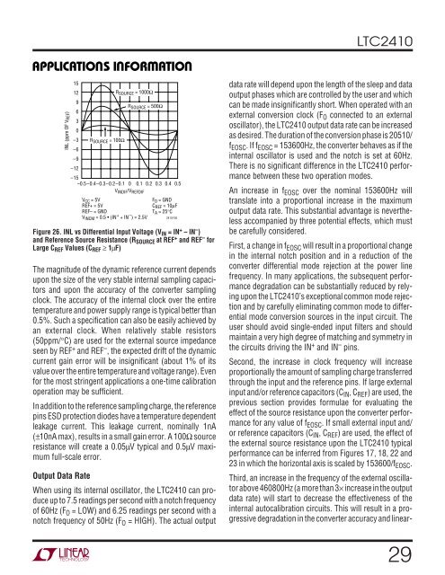
<strong>LTC<strong>24</strong>10</strong>APPLICATIO S I FORINL (ppm OF V REF )15129630–3–6–9–12ATIOU W U UR SOURCE = 100ΩR SOURCE = 1000ΩR SOURCE = 500Ω–15–0.5–0.4–0.3–0.2–0.1 0 0.1 0.2 0.3 0.4 0.5V INDIF /V REFDIFV CC = 5VREF+ = 5VREF– = GNDV INCM = 0.5 • (IN + + IN – ) = 2.5VF O = GNDC REF = 10µFT A = 25°C<strong>24</strong>10 F26Figure 26. INL vs <strong>Differential</strong> <strong>Input</strong> Voltage (V IN = IN + – IN – )<strong>and</strong> Reference Source Resistance (R SOURCE at REF + <strong>and</strong> REF – forLarge C REF Values (C REF ≥ 1µF)The magnitude of the dynamic reference current dependsupon the size of the very stable internal sampling capacitors<strong>and</strong> upon the accuracy of the converter samplingclock. The accuracy of the internal clock over the entiretemperature <strong>and</strong> power supply range is typical better than0.5%. Such a specification can also be easily achieved byan external clock. When relatively stable resistors(50ppm/°C) are used for the external source impedanceseen by REF + <strong>and</strong> REF – , the expected drift of the dynamiccurrent gain error will be insignificant (about 1% of itsvalue over the entire temperature <strong>and</strong> voltage range). Evenfor the most stringent applications a one-time calibrationoperation may be sufficient.In addition to the reference sampling charge, the referencepins ESD protection diodes have a temperature dependentleakage current. This leakage current, nominally 1nA(±10nA max), results in a small gain error. A 100Ω sourceresistance will create a 0.05µV typical <strong>and</strong> 0.5µV maximumfull-scale error.Output Data RateWhen using its internal oscillator, the <strong>LTC<strong>24</strong>10</strong> can produceup to 7.5 readings per second <strong>with</strong> a notch frequencyof 60Hz (F O = LOW) <strong>and</strong> 6.25 readings per second <strong>with</strong> anotch frequency of 50Hz (F O = HIGH). The actual outputdata rate will depend upon the length of the sleep <strong>and</strong> dataoutput phases which are controlled by the user <strong>and</strong> whichcan be made insignificantly short. When operated <strong>with</strong> anexternal conversion clock (F O connected to an externaloscillator), the <strong>LTC<strong>24</strong>10</strong> output data rate can be increasedas desired. The duration of the conversion phase is 20510/f EOSC . If f EOSC = 153600Hz, the converter behaves as if theinternal oscillator is used <strong>and</strong> the notch is set at 60Hz.There is no significant difference in the <strong>LTC<strong>24</strong>10</strong> performancebetween these two operation modes.An increase in f EOSC over the nominal 153600Hz willtranslate into a proportional increase in the maximumoutput data rate. This substantial advantage is neverthelessaccompanied by three potential effects, which mustbe carefully considered.First, a change in f EOSC will result in a proportional changein the internal notch position <strong>and</strong> in a reduction of theconverter differential mode rejection at the power linefrequency. In many applications, the subsequent performancedegradation can be substantially reduced by relyingupon the <strong>LTC<strong>24</strong>10</strong>’s exceptional common mode rejection<strong>and</strong> by carefully eliminating common mode to differentialmode conversion sources in the input circuit. Theuser should avoid single-ended input filters <strong>and</strong> shouldmaintain a very high degree of matching <strong>and</strong> symmetry inthe circuits driving the IN + <strong>and</strong> IN – pins.Second, the increase in clock frequency will increaseproportionally the amount of sampling charge transferredthrough the input <strong>and</strong> the reference pins. If large externalinput <strong>and</strong>/or reference capacitors (C IN , C REF ) are used, theprevious section provides formulae for evaluating theeffect of the source resistance upon the converter performancefor any value of f EOSC . If small external input <strong>and</strong>/or reference capacitors (C IN , C REF ) are used, the effect ofthe external source resistance upon the <strong>LTC<strong>24</strong>10</strong> typicalperformance can be inferred from Figures 17, 18, 22 <strong>and</strong>23 in which the horizontal axis is scaled by 153600/f EOSC .Third, an increase in the frequency of the external oscillatorabove 460800Hz (a more than 3× increase in the outputdata rate) will start to decrease the effectiveness of theinternal autocalibration circuits. This will result in a progressivedegradation in the converter accuracy <strong>and</strong> linear-29