LTC2410 24-Bit No Latency âΣTM ADC with Differential Input and ...
LTC2410 24-Bit No Latency âΣTM ADC with Differential Input and ...
LTC2410 24-Bit No Latency âΣTM ADC with Differential Input and ...

Create successful ePaper yourself
Turn your PDF publications into a flip-book with our unique Google optimized e-Paper software.
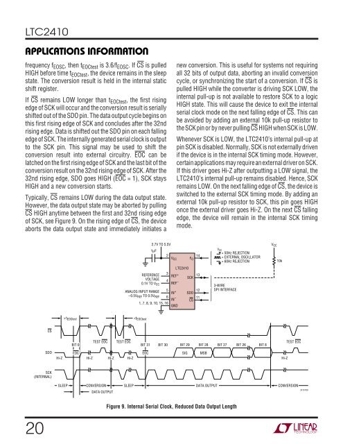
<strong>LTC<strong>24</strong>10</strong>APPLICATIO S I FORATIOU W U Ufrequency f EOSC , then t EOCtest is 3.6/f EOSC . If CS is pulledHIGH before time t EOCtest , the device remains in the sleepstate. The conversion result is held in the internal staticshift register.If CS remains LOW longer than t EOCtest , the first risingedge of SCK will occur <strong>and</strong> the conversion result is seriallyshifted out of the SDO pin. The data output cycle begins onthis first rising edge of SCK <strong>and</strong> concludes after the 32ndrising edge. Data is shifted out the SDO pin on each fallingedge of SCK. The internally generated serial clock is outputto the SCK pin. This signal may be used to shift theconversion result into external circuitry. EOC can belatched on the first rising edge of SCK <strong>and</strong> the last bit of theconversion result on the 32nd rising edge of SCK. After the32nd rising edge, SDO goes HIGH (EOC = 1), SCK staysHIGH <strong>and</strong> a new conversion starts.Typically, CS remains LOW during the data output state.However, the data output state may be aborted by pullingCS HIGH anytime between the first <strong>and</strong> 32nd rising edgeof SCK, see Figure 9. On the rising edge of CS, the deviceaborts the data output state <strong>and</strong> immediately initiates anew conversion. This is useful for systems not requiringall 32 bits of output data, aborting an invalid conversioncycle, or synchronizing the start of a conversion. If CS ispulled HIGH while the converter is driving SCK LOW, theinternal pull-up is not available to restore SCK to a logicHIGH state. This will cause the device to exit the internalserial clock mode on the next falling edge of CS. This canbe avoided by adding an external 10k pull-up resistor tothe SCK pin or by never pulling CS HIGH when SCK is LOW.Whenever SCK is LOW, the <strong>LTC<strong>24</strong>10</strong>’s internal pull-up atpin SCK is disabled. <strong>No</strong>rmally, SCK is not externally drivenif the device is in the internal SCK timing mode. However,certain applications may require an external driver on SCK.If this driver goes Hi-Z after outputting a LOW signal, the<strong>LTC<strong>24</strong>10</strong>’s internal pull-up remains disabled. Hence, SCKremains LOW. On the next falling edge of CS, the device isswitched to the external SCK timing mode. By adding anexternal 10k pull-up resistor to SCK, this pin goes HIGHonce the external driver goes Hi-Z. On the next CS fallingedge, the device will remain in the internal SCK timingmode.2.7V TO 5.5VV CCV1µFCC= 50Hz REJECTION2 14V = EXTERNAL OSCILLATORCC F O= 60Hz REJECTION10k<strong>LTC<strong>24</strong>10</strong>REFERENCE3REF + 13VOLTAGESCK40.1V TO V REF –CC3-WIRE5IN +12 SPI INTERFACEANALOG INPUT RANGESDO–0.5V REF TO 0.5V REF 6IN –11CS1, 7, 8, 9, 10, 15, 16GNDt EOCtestMSBCSBIT 0TEST EOCTEST EOCBIT 31BIT 30BIT 29BIT 28BIT 27 BIT 26BIT 8TEST EOCSDOEOCEOCSIGHi-Z Hi-Z Hi-Z Hi-Z Hi-ZSCK(INTERNAL)SLEEPCONVERSIONSLEEPDATA OUTPUTCONVERSIONDATA OUTPUT<strong>24</strong>10 F0920Figure 9. Internal Serial Clock, Reduced Data Output Length