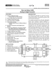
LTC2410 24-Bit No Latency âΣTM ADC with Differential Input and ...
LTC2410 24-Bit No Latency âΣTM ADC with Differential Input and ...
LTC2410 24-Bit No Latency âΣTM ADC with Differential Input and ...

You also want an ePaper? Increase the reach of your titles
YUMPU automatically turns print PDFs into web optimized ePapers that Google loves.
<strong>LTC<strong>24</strong>10</strong>APPLICATIO S I FOROnce CS is pulled LOW, the device begins outputting theconversion result. There is no latency in the conversionresult. The data output corresponds to the conversion justperformed. This result is shifted out on the serial data outpin (SDO) under the control of the serial clock (SCK). Datais updated on the falling edge of SCK allowing the user toreliably latch data on the rising edge of SCK (see Figure 3).The data output state is concluded once 32 bits are readout of the <strong>ADC</strong> or when CS is brought HIGH. The deviceautomatically initiates a new conversion <strong>and</strong> the cyclerepeats.Through timing control of the CS <strong>and</strong> SCK pins, the<strong>LTC<strong>24</strong>10</strong> offers several flexible modes of operation(internal or external SCK <strong>and</strong> free-running conversionmodes). These various modes do not require programmingconfiguration registers; moreover, they do not disturbthe cyclic operation described above. These modes ofoperation are described in detail in the Serial InterfaceTiming Modes section.Conversion ClockA major advantage the delta-sigma converter offers overconventional type converters is an on-chip digital filter(commonly implemented as a Sinc or Comb filter). Forhigh resolution, low frequency applications, this filter istypically designed to reject line frequencies of 50 or 60Hzplus their harmonics. The filter rejection performance isdirectly related to the accuracy of the converter systemclock. The <strong>LTC<strong>24</strong>10</strong> incorporates a highly accurate onchiposcillator. This eliminates the need for external frequencysetting components such as crystals or oscillators.Clocked by the on-chip oscillator, the <strong>LTC<strong>24</strong>10</strong>achieves a minimum of 110dB rejection at the line frequency(50Hz or 60Hz ±2%).Ease of UseThe <strong>LTC<strong>24</strong>10</strong> data output has no latency, filter settlingdelay or redundant data associated <strong>with</strong> the conversioncycle. There is a one-to-one correspondence between theconversion <strong>and</strong> the output data. Therefore, multiplexingmultiple analog voltages is easy.12ATIOU W U UThe <strong>LTC<strong>24</strong>10</strong> performs offset <strong>and</strong> full-scale calibrationsevery conversion cycle. This calibration is transparent tothe user <strong>and</strong> has no effect on the cyclic operation describedabove. The advantage of continuous calibration isextreme stability of offset <strong>and</strong> full-scale readings <strong>with</strong> respectto time, supply voltage change <strong>and</strong> temperature drift.Power-Up SequenceThe <strong>LTC<strong>24</strong>10</strong> automatically enters an internal reset statewhen the power supply voltage V CC drops below approximately2.2V. This feature guarantees the integrity of theconversion result <strong>and</strong> of the serial interface mode selection.(See the 2-wire I/O sections in the Serial InterfaceTiming Modes section.)When the V CC voltage rises above this critical threshold,the converter creates an internal power-on-reset (POR)signal <strong>with</strong> a duration of approximately 0.5ms. The PORsignal clears all internal registers. Following the PORsignal, the <strong>LTC<strong>24</strong>10</strong> starts a normal conversion cycle <strong>and</strong>follows the succession of states described above. The firstconversion result following POR is accurate <strong>with</strong>in thespecifications of the device if the power supply voltage isrestored <strong>with</strong>in the operating range (2.7V to 5.5V) beforethe end of the POR time interval.Reference Voltage RangeThis converter accepts a truly differential external referencevoltage. The absolute/common mode voltage specificationfor the REF + <strong>and</strong> REF – pins covers the entire rangefrom GND to V CC . For correct converter operation, theREF + pin must always be more positive than the REF – pin.The <strong>LTC<strong>24</strong>10</strong> can accept a differential reference voltagefrom 0.1V to V CC . The converter output noise is determinedby the thermal noise of the front-end circuits, <strong>and</strong>as such, its value in nanovolts is nearly constant <strong>with</strong>reference voltage. A decrease in reference voltage will notsignificantly improve the converter’s effective resolution.On the other h<strong>and</strong>, a reduced reference voltage will improvethe converter’s overall INL performance. A reducedreference voltage will also improve the converter performancewhen operated <strong>with</strong> an external conversion clock(external F O signal) at substantially higher output datarates (see the Output Data Rate section).