LTC2410 24-Bit No Latency âΣTM ADC with Differential Input and ...
LTC2410 24-Bit No Latency âΣTM ADC with Differential Input and ...
LTC2410 24-Bit No Latency âΣTM ADC with Differential Input and ...

You also want an ePaper? Increase the reach of your titles
YUMPU automatically turns print PDFs into web optimized ePapers that Google loves.
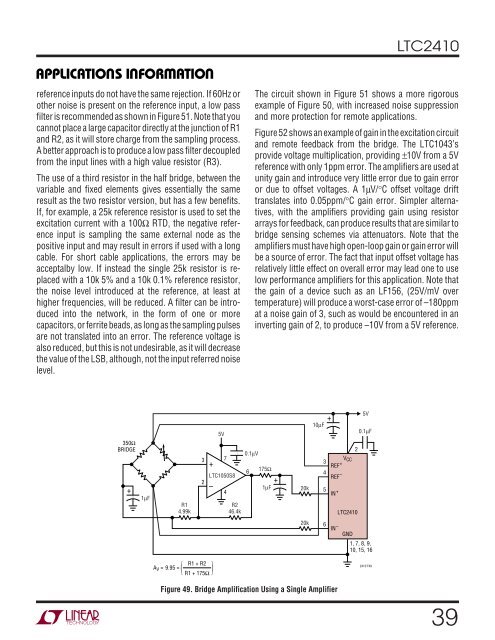
<strong>LTC<strong>24</strong>10</strong>APPLICATIO S I FORATIOU W U Ureference inputs do not have the same rejection. If 60Hz orother noise is present on the reference input, a low passfilter is recommended as shown in Figure 51. <strong>No</strong>te that youcannot place a large capacitor directly at the junction of R1<strong>and</strong> R2, as it will store charge from the sampling process.A better approach is to produce a low pass filter decoupledfrom the input lines <strong>with</strong> a high value resistor (R3).The use of a third resistor in the half bridge, between thevariable <strong>and</strong> fixed elements gives essentially the sameresult as the two resistor version, but has a few benefits.If, for example, a 25k reference resistor is used to set theexcitation current <strong>with</strong> a 100Ω RTD, the negative referenceinput is sampling the same external node as thepositive input <strong>and</strong> may result in errors if used <strong>with</strong> a longcable. For short cable applications, the errors may beacceptalby low. If instead the single 25k resistor is replaced<strong>with</strong> a 10k 5% <strong>and</strong> a 10k 0.1% reference resistor,the noise level introduced at the reference, at least athigher frequencies, will be reduced. A filter can be introducedinto the network, in the form of one or morecapacitors, or ferrite beads, as long as the sampling pulsesare not translated into an error. The reference voltage isalso reduced, but this is not undesirable, as it will decreasethe value of the LSB, although, not the input referred noiselevel.The circuit shown in Figure 51 shows a more rigorousexample of Figure 50, <strong>with</strong> increased noise suppression<strong>and</strong> more protection for remote applications.Figure 52 shows an example of gain in the excitation circuit<strong>and</strong> remote feedback from the bridge. The LTC1043’sprovide voltage multiplication, providing ±10V from a 5Vreference <strong>with</strong> only 1ppm error. The amplifiers are used atunity gain <strong>and</strong> introduce very little error due to gain erroror due to offset voltages. A 1µV/°C offset voltage drifttranslates into 0.05ppm/°C gain error. Simpler alternatives,<strong>with</strong> the amplifiers providing gain using resistorarrays for feedback, can produce results that are similar tobridge sensing schemes via attenuators. <strong>No</strong>te that theamplifiers must have high open-loop gain or gain error willbe a source of error. The fact that input offset voltage hasrelatively little effect on overall error may lead one to uselow performance amplifiers for this application. <strong>No</strong>te thatthe gain of a device such as an LF156, (25V/mV overtemperature) will produce a worst-case error of –180ppmat a noise gain of 3, such as would be encountered in aninverting gain of 2, to produce –10V from a 5V reference.350ΩBRIDGE+1µFR14.99k32+–5V7LTC1050S84R<strong>24</strong>6.4k0.1µV6175Ω1µF+20k10µFV3 CCREF +4REF –5+IN +2<strong>LTC<strong>24</strong>10</strong>5V0.1µFR1 + R2A V = 9.95 =( )R1 + 175Ω20k6IN –GND1, 7, 8, 9,10, 15, 16<strong>24</strong>10 F49Figure 49. Bridge Amplification Using a Single Amplifier39