LTC2410 24-Bit No Latency âΣTM ADC with Differential Input and ...
LTC2410 24-Bit No Latency âΣTM ADC with Differential Input and ...
LTC2410 24-Bit No Latency âΣTM ADC with Differential Input and ...

Create successful ePaper yourself
Turn your PDF publications into a flip-book with our unique Google optimized e-Paper software.
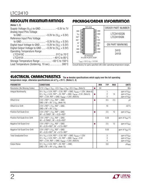
<strong>LTC<strong>24</strong>10</strong>ABSOLUTE AXI U RATI GSW W W(<strong>No</strong>tes 1, 2)Supply Voltage (V CC ) to GND.......................–0.3V to 7VAnalog <strong>Input</strong> Pins Voltageto GND .................................... –0.3V to (V CC + 0.3V)Reference <strong>Input</strong> Pins Voltageto GND .................................... –0.3V to (V CC + 0.3V)Digital <strong>Input</strong> Voltage to GND ........ –0.3V to (V CC + 0.3V)Digital Output Voltage to GND ..... –0.3V to (V CC + 0.3V)Operating Temperature Range<strong>LTC<strong>24</strong>10</strong>C ............................................... 0°C to 70°C<strong>LTC<strong>24</strong>10</strong>I............................................ –40°C to 85°CStorage Temperature Range ................. –65°C to 150°CLead Temperature (Soldering, 10 sec).................. 300°CUU U WPACKAGE/ORDER I FOR ATIOGNDV CCREF +REF –IN +IN –GNDGND12345678TOP VIEW161514131211109GN PACKAGE16-LEAD PLASTIC SSOPT JMAX = 125°C, θ JA = 110°C/WGNDGNDF OSCKSDOCSGNDGNDORDER PART NUMBER<strong>LTC<strong>24</strong>10</strong>CGN<strong>LTC<strong>24</strong>10</strong>IGNGN PART MARKING<strong>24</strong>10<strong>24</strong>10IConsult factory for parts specified <strong>with</strong> wider operating temperature ranges.ELECTRICAL CHARACTERISTICSThe ● denotes specifications which apply over the full operatingtemperature range, otherwise specifications are at T A = 25°C. (<strong>No</strong>tes 3, 4)PARAMETER CONDITIONS MIN TYP MAX UNITSResolution (<strong>No</strong> Missing Codes) 0.1V ≤ V REF ≤ V CC , –0.5 • V REF ≤ V IN ≤ 0.5 • V REF , (<strong>No</strong>te 5) ● <strong>24</strong> <strong>Bit</strong>sIntegral <strong>No</strong>nlinearity 5V ≤ V CC ≤ 5.5V, REF + = 2.5V, REF – = GND, V INCM = 1.25V, (<strong>No</strong>te 6) 1 ppm of V REF5V ≤ V CC ≤ 5.5V, REF + = 5V, REF – = GND, V INCM = 2.5V, (<strong>No</strong>te 6) ● 2 14 ppm of V REFREF + = 2.5V, REF – = GND, V INCM = 1.25V, (<strong>No</strong>te 6) 5 ppm of V REFOffset Error 2.5V ≤ REF + ≤ V CC , REF – = GND, ● 0.5 2.5 µVGND ≤ IN + = IN – ≤ V CC , (<strong>No</strong>te 14)Offset Error Drift 2.5V ≤ REF + ≤ V CC , REF – = GND, 10 nV/°CGND ≤ IN + = IN – ≤ V CCPositive Full-Scale Error 2.5V ≤ REF + ≤ V CC , REF – = GND, ● 2.5 12 ppm of V REFIN + = 0.75REF + , IN – = 0.25 • REF +Positive Full-Scale Error Drift 2.5V ≤ REF + ≤ V CC , REF – = GND, 0.03 ppm of V REF /°CIN + = 0.75REF + , IN – = 0.25 • REF +Negative Full-Scale Error 2.5V ≤ REF + ≤ V CC , REF – = GND, ● 2.5 12 ppm of V REFIN + = 0.25 • REF + , IN – = 0.75 • REF +Negative Full-Scale Error Drift 2.5V ≤ REF + ≤ V CC , REF – = GND, 0.03 ppm of V REF /°CIN + = 0.25 • REF + , IN – = 0.75 • REF +Total Unadjusted Error 5V ≤ V CC ≤ 5.5V, REF + = 2.5V, REF – = GND, V INCM = 1.25V 3 ppm of V REF5V ≤ V CC ≤ 5.5V, REF + = 5V, REF – = GND, V INCM = 2.5V 3 ppm of V REFREF + = 2.5V, REF – = GND, V INCM = 1.25V, (<strong>No</strong>te 6) 4 ppm of V REFOutput <strong>No</strong>ise 5V ≤ V CC ≤ 5.5V, REF + = 5V, REF – = GND, 0.8 µV RMSGND ≤ IN – = IN + ≤ V CC , (<strong>No</strong>te 13)2