LTC2410 24-Bit No Latency âΣTM ADC with Differential Input and ...
LTC2410 24-Bit No Latency âΣTM ADC with Differential Input and ...
LTC2410 24-Bit No Latency âΣTM ADC with Differential Input and ...

You also want an ePaper? Increase the reach of your titles
YUMPU automatically turns print PDFs into web optimized ePapers that Google loves.
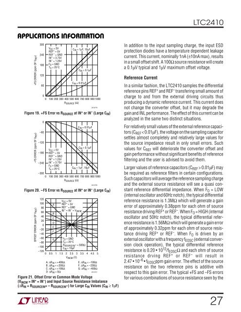
<strong>LTC<strong>24</strong>10</strong>APPLICATIO S I FOR+FS ERROR (ppm OF VREF)300<strong>24</strong>0180120600ATIOU W U UV CC = 5VREF + = 5VREF – = GNDIN + = 3.75VIN – = 1.25VF O = GNDT A = 25°CC IN = 1µF, 10µFC IN = 0.1µFC IN = 0.01µF0 100 200 300 400 500 600 700 800 900 1000R SOURCE (Ω)<strong>24</strong>10 F19Figure 19. +FS Error vs R SOURCE at IN + or IN – (Large C IN )–FS ERROR (ppm OF VREF)0–60–120–180–<strong>24</strong>0–300V CC = 5VREF + = 5VREF – = GNDIN + = 1.25VIN – = 3.75VF O = GNDT A = 25°CC IN = 0.01µFC IN = 0.1µFC IN = 1µF, 10µF0 100 200 300 400 500 600 700 800 900 1000R SOURCE (Ω)<strong>24</strong>10 F20Figure 20. –FS Error vs R SOURCE at IN + or IN – (Large C IN )OFFSET ERROR (ppm OF V REF )120100806040200–20–40–60–80–100–120ABCDEFGV CC = 5VREF + = 5VREF – = GNDIN + = IN – = V INCMF O = GNDT A = 25°CR SOURCEIN – = 500ΩC IN = 10µF0 0.5 1 1.5 2 2.5 3 3.5 4 4.5 5V INCM (V)A: ∆R IN = +400ΩB: ∆R IN = +200ΩC: ∆R IN = +100ΩD: ∆R IN = 0ΩE: ∆R IN = –100ΩF: ∆R IN = –200ΩG: ∆R IN = –400Ω<strong>24</strong>10 F21Figure 21. Offset Error vs Common Mode Voltage(V INCM = IN + = IN – ) <strong>and</strong> <strong>Input</strong> Source Resistance Imbalance(∆R IN = R SOURCEIN + – R SOURCEIN –) for Large C IN Values (C IN ≥ 1µF)In addition to the input sampling charge, the input ESDprotection diodes have a temperature dependent leakagecurrent. This current, nominally 1nA (±10nA max), resultsin a small offset shift. A 100Ω source resistance will createa 0.1µV typical <strong>and</strong> 1µV maximum offset voltage.Reference CurrentIn a similar fashion, the <strong>LTC<strong>24</strong>10</strong> samples the differentialreference pins REF + <strong>and</strong> REF – transfering small amount ofcharge to <strong>and</strong> from the external driving circuits thusproducing a dynamic reference current. This current doesnot change the converter offset, but it may degrade thegain <strong>and</strong> INL performance. The effect of this current can beanalyzed in the same two distinct situations.For relatively small values of the external reference capacitors(C REF < 0.01µF), the voltage on the sampling capacitorsettles almost completely <strong>and</strong> relatively large values forthe source impedance result in only small errors. Suchvalues for C REF will deteriorate the converter offset <strong>and</strong>gain performance <strong>with</strong>out significant benefits of referencefiltering <strong>and</strong> the user is advised to avoid them.Larger values of reference capacitors (C REF > 0.01µF) maybe required as reference filters in certain configurations.Such capacitors will average the reference sampling charge<strong>and</strong> the external source resistance will see a quasi constantreference differential impedance. When F O = LOW(internal oscillator <strong>and</strong> 60Hz notch), the typical differentialreference resistance is 1.3MΩ which will generate a gainerror of approximately 0.38ppm for each ohm of sourceresistance driving REF + or REF – . When F O = HIGH (internaloscillator <strong>and</strong> 50Hz notch), the typical differential referenceresistance is 1.56MΩ which will generate a gain errorof approximately 0.32ppm for each ohm of source resistancedriving REF + or REF – . When F O is driven by anexternal oscillator <strong>with</strong> a frequency f EOSC (external conversionclock operation), the typical differential referenceresistance is 0.20 • 10 12 /f EOSC Ω <strong>and</strong> each ohm of sourceresistance drving REF + or REF – will result in2.47 • 10 –6 • f EOSC ppm gain error. The effect of the sourceresistance on the two reference pins is additive <strong>with</strong>respect to this gain error. The typical +FS <strong>and</strong> –FS errorsfor various combinations of source resistance seen by the27