LTC2410 24-Bit No Latency âΣTM ADC with Differential Input and ...
LTC2410 24-Bit No Latency âΣTM ADC with Differential Input and ...
LTC2410 24-Bit No Latency âΣTM ADC with Differential Input and ...

You also want an ePaper? Increase the reach of your titles
YUMPU automatically turns print PDFs into web optimized ePapers that Google loves.
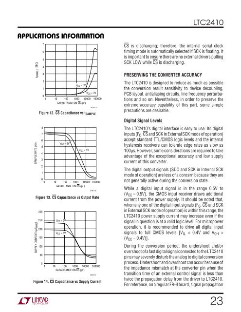
<strong>LTC<strong>24</strong>10</strong>APPLICATIO S I FORSAMPLE RATE (Hz)t SAMPLE (SEC)SUPPLY CURRENT (µA RMS )765432101ATIOU W U UV CC = 5VV CC = 3V10 100 1000 10000 100000CAPACITANCE ON CS (pF)<strong>24</strong>00 F12Figure 12. CS Capacitance vs t SAMPLE876V CC = 5V5V CC = 3V432100 10 100 1000 10000 100000CAPACITANCE ON CS (pF)<strong>24</strong>00 F13Figure 13. CS Capacitance vs Output Rate300250 V CC = 5V200V CC = 3V1501005001 10 100 1000 10000 100000CAPACITANCE ON CS (pF)<strong>24</strong>00 F14Figure 14. CS Capacitance vs Supply CurrentCS is discharging; therefore, the internal serial clocktiming mode is automatically selected if SCK is floating. Itis important to ensure there are no external drivers pullingSCK LOW while CS is discharging.PRESERVING THE CONVERTER ACCURACYThe <strong>LTC<strong>24</strong>10</strong> is designed to reduce as much as possiblethe conversion result sensitivity to device decoupling,PCB layout, antialiasing circuits, line frequency perturbations<strong>and</strong> so on. Nevertheless, in order to preserve theextreme accuracy capability of this part, some simpleprecautions are desirable.Digital Signal LevelsThe <strong>LTC<strong>24</strong>10</strong>’s digital interface is easy to use. Its digitalinputs (F O , CS <strong>and</strong> SCK in External SCK mode of operation)accept st<strong>and</strong>ard TTL/CMOS logic levels <strong>and</strong> the internalhysteresis receivers can tolerate edge rates as slow as100µs. However, some considerations are required to takeadvantage of the exceptional accuracy <strong>and</strong> low supplycurrent of this converter.The digital output signals (SDO <strong>and</strong> SCK in Internal SCKmode of operation) are less of a concern because they arenot generally active during the conversion state.While a digital input signal is in the range 0.5V to(V CC ␣ –␣ 0.5V), the CMOS input receiver draws additionalcurrent from the power supply. It should be noted that,when any one of the digital input signals (F O , CS <strong>and</strong> SCKin External SCK mode of operation) is <strong>with</strong>in this range, the<strong>LTC<strong>24</strong>10</strong> power supply current may increase even if thesignal in question is at a valid logic level. For micropoweroperation, it is recommended to drive all digital inputsignals to full CMOS levels [V IL < 0.4V <strong>and</strong> V OH >(V CC – 0.4V)].During the conversion period, the undershoot <strong>and</strong>/orovershoot of a fast digital signal connected to the <strong>LTC<strong>24</strong>10</strong>pins may severely disturb the analog to digital conversionprocess. Undershoot <strong>and</strong> overshoot can occur because ofthe impedance mismatch at the converter pin when thetransition time of an external control signal is less thantwice the propagation delay from the driver to <strong>LTC<strong>24</strong>10</strong>.For reference, on a regular FR-4 board, signal propagation23