LTC2410 24-Bit No Latency âΣTM ADC with Differential Input and ...
LTC2410 24-Bit No Latency âΣTM ADC with Differential Input and ...
LTC2410 24-Bit No Latency âΣTM ADC with Differential Input and ...

You also want an ePaper? Increase the reach of your titles
YUMPU automatically turns print PDFs into web optimized ePapers that Google loves.
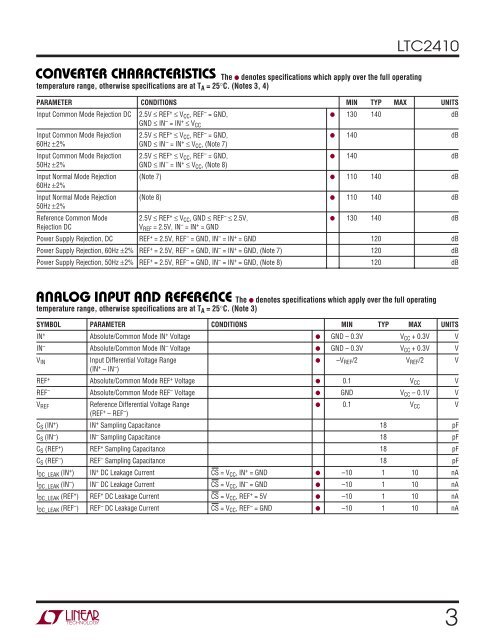
CO VERTER CHARACTERISTICSUThe ● denotes specifications which apply over the full operatingtemperature range, otherwise specifications are at T A = 25°C. (<strong>No</strong>tes 3, 4)<strong>LTC<strong>24</strong>10</strong>PARAMETER CONDITIONS MIN TYP MAX UNITS<strong>Input</strong> Common Mode Rejection DC 2.5V ≤ REF + ≤ V CC , REF – = GND, ● 130 140 dBGND ≤ IN – = IN + ≤ V CC<strong>Input</strong> Common Mode Rejection 2.5V ≤ REF + ≤ V CC , REF – = GND, ● 140 dB60Hz ±2% GND ≤ IN – = IN + ≤ V CC , (<strong>No</strong>te 7)<strong>Input</strong> Common Mode Rejection 2.5V ≤ REF + ≤ V CC , REF – = GND, ● 140 dB50Hz ±2% GND ≤ IN – = IN + ≤ V CC , (<strong>No</strong>te 8)<strong>Input</strong> <strong>No</strong>rmal Mode Rejection (<strong>No</strong>te 7) ● 110 140 dB60Hz ±2%<strong>Input</strong> <strong>No</strong>rmal Mode Rejection (<strong>No</strong>te 8) ● 110 140 dB50Hz ±2%Reference Common Mode 2.5V ≤ REF + ≤ V CC , GND ≤ REF – ≤ 2.5V, ● 130 140 dBRejection DCV REF = 2.5V, IN – = IN + = GNDPower Supply Rejection, DC REF + = 2.5V, REF – = GND, IN – = IN + = GND 120 dBPower Supply Rejection, 60Hz ±2% REF + = 2.5V, REF – = GND, IN – = IN + = GND, (<strong>No</strong>te 7) 120 dBPower Supply Rejection, 50Hz ±2% REF + = 2.5V, REF – = GND, IN – = IN + = GND, (<strong>No</strong>te 8) 120 dBUU UUA ALOG I PUT A D REFERE CEThe ● denotes specifications which apply over the full operatingtemperature range, otherwise specifications are at T A = 25°C. (<strong>No</strong>te 3)SYMBOL PARAMETER CONDITIONS MIN TYP MAX UNITSIN + Absolute/Common Mode IN + Voltage ● GND – 0.3V V CC + 0.3V VIN – Absolute/Common Mode IN – Voltage ● GND – 0.3V V CC + 0.3V VV IN <strong>Input</strong> <strong>Differential</strong> Voltage Range ● –V REF /2 V REF /2 V(IN + – IN – )REF + Absolute/Common Mode REF + Voltage ● 0.1 V CC VREF – Absolute/Common Mode REF – Voltage ● GND V CC – 0.1V VV REF Reference <strong>Differential</strong> Voltage Range ● 0.1 V CC V(REF + – REF – )C S (IN + ) IN + Sampling Capacitance 18 pFC S (IN – ) IN – Sampling Capacitance 18 pFC S (REF + ) REF + Sampling Capacitance 18 pFC S (REF – ) REF – Sampling Capacitance 18 pFI DC_LEAK (IN + ) IN + DC Leakage Current CS = V CC , IN + = GND ● –10 1 10 nAI DC_LEAK (IN – ) IN – DC Leakage Current CS = V CC , IN – = GND ● –10 1 10 nAI DC_LEAK (REF + ) REF + DC Leakage Current CS = V CC , REF + = 5V ● –10 1 10 nAI DC_LEAK (REF – ) REF – DC Leakage Current CS = V CC , REF – = GND ● –10 1 10 nA3