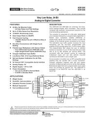
LTC2410 24-Bit No Latency âΣTM ADC with Differential Input and ...
LTC2410 24-Bit No Latency âΣTM ADC with Differential Input and ...
LTC2410 24-Bit No Latency âΣTM ADC with Differential Input and ...

You also want an ePaper? Increase the reach of your titles
YUMPU automatically turns print PDFs into web optimized ePapers that Google loves.
<strong>LTC<strong>24</strong>10</strong>APPLICATIO S I FORATIOU W U U<strong>Input</strong> Voltage RangeThe analog input is truly differential <strong>with</strong> an absolute/common mode range for the IN + <strong>and</strong> IN – input pinsextending from GND – 0.3V to V CC + 0.3V. Outsidethese limits, the ESD protection devices begin to turn on<strong>and</strong> the errors due to input leakage current increaserapidly. Within these limits, the <strong>LTC<strong>24</strong>10</strong> converts thebipolar differential input signal, V IN = IN + – IN – , from–FS = –0.5 • V REF to +FS = 0.5 • V REF where V REF =REF + – REF – . Outside this range, the converter indicatesthe overrange or the underrange condition using distinctoutput codes.<strong>Input</strong> signals applied to IN + <strong>and</strong> IN – pins may extend by300mV below ground <strong>and</strong> above V CC . In order to limit anyfault current, resistors of up to 5k may be added in series<strong>with</strong> the IN + <strong>and</strong> IN – pins <strong>with</strong>out affecting the performanceof the device. In the physical layout, it is importantto maintain the parasitic capacitance of the connectionbetween these series resistors <strong>and</strong> the corresponding pinsas low as possible; therefore, the resistors should belocated as close as practical to the pins. The effect of theseries resistance on the converter accuracy can be evaluatedfrom the curves presented in the <strong>Input</strong> Current/Reference Current sections. In addition, series resistorswill introduce a temperature dependent offset error due tothe input leakage current. A 1nA input leakage current willdevelop a 1ppm offset error on a 5k resistor if V REF = 5V.This error has a very strong temperature dependency.Output Data FormatThe <strong>LTC<strong>24</strong>10</strong> serial output data stream is 32 bits long. Thefirst 3 bits represent status information indicating the sign<strong>and</strong> conversion state. The next <strong>24</strong> bits are the conversionresult, MSB first. The remaining 5 bits are sub LSBsbeyond the <strong>24</strong>-bit level that may be included in averagingor discarded <strong>with</strong>out loss of resolution. The third <strong>and</strong>fourth bit together are also used to indicate an underrangecondition (the differential input voltage is below –FS) or anoverrange condition (the differential input voltage is above+FS).<strong>Bit</strong> 31 (first output bit) is the end of conversion (EOC)indicator. This bit is available at the SDO pin during theconversion <strong>and</strong> sleep states whenever the CS pin is LOW.This bit is HIGH during the conversion <strong>and</strong> goes LOWwhen the conversion is complete.<strong>Bit</strong> 30 (second output bit) is a dummy bit (DMY) <strong>and</strong> isalways LOW.<strong>Bit</strong> 29 (third output bit) is the conversion result sign indicator(SIG). If V IN is >0, this bit is HIGH. If V IN is