LTC2410 24-Bit No Latency âΣTM ADC with Differential Input and ...
LTC2410 24-Bit No Latency âΣTM ADC with Differential Input and ...
LTC2410 24-Bit No Latency âΣTM ADC with Differential Input and ...

Create successful ePaper yourself
Turn your PDF publications into a flip-book with our unique Google optimized e-Paper software.
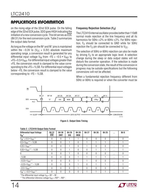
<strong>LTC<strong>24</strong>10</strong>APPLICATIO S I FORATIOU W U Uon the rising edge of the 32nd SCK pulse. On the fallingedge of the 32nd SCK pulse, SDO goes HIGH indicating theinitiation of a new conversion cycle. This bit serves as EOC(<strong>Bit</strong> 31) for the next conversion cycle. Table 2 summarizesthe output data format.As long as the voltage on the IN + <strong>and</strong> IN – pins is maintained<strong>with</strong>in the – 0.3V to (V CC + 0.3V) absolute maximumoperating range, a conversion result is generated for anydifferential input voltage V IN from –FS = –0.5 • V REF to+FS = 0.5 • V REF . For differential input voltages greater than+FS, the conversion result is clamped to the value correspondingto the +FS + 1LSB. For differential input voltagesbelow –FS, the conversion result is clamped to the valuecorresponding to –FS – 1LSB.Frequency Rejection Selection (F O )The <strong>LTC<strong>24</strong>10</strong> internal oscillator provides better than 110dBnormal mode rejection at the line frequency <strong>and</strong> all itsharmonics for 50Hz ±2% or 60Hz ±2%. For 60Hz rejection,F O should be connected to GND while for 50Hzrejection the F O pin should be connected to V CC .The selection of 50Hz or 60Hz rejection can also be madeby driving F O to an appropriate logic level. A selectionchange during the sleep or data output states will notdisturb the converter operation. If the selection is madeduring the conversion state, the result of the conversion inprogress may be outside specifications but the followingconversions will not be affected.When a fundamental rejection frequency different from50Hz or 60Hz is required or when the converter must beCSBIT 31BIT 30BIT 29BIT 28BIT 27 BIT 5BIT 0SDOHi-ZEOC“0”SIGMSBLSB <strong>24</strong>SCK1 2 3 4 5 26 27 32SLEEP DATA OUTPUT CONVERSIONFigure 3. Output Data Timing<strong>24</strong>10 F0314Table 2. <strong>LTC<strong>24</strong>10</strong> Output Data Format<strong>Differential</strong> <strong>Input</strong> Voltage <strong>Bit</strong> 31 <strong>Bit</strong> 30 <strong>Bit</strong> 29 <strong>Bit</strong> 28 <strong>Bit</strong> 27 <strong>Bit</strong> 26 <strong>Bit</strong> 25 … <strong>Bit</strong> 0V IN * EOC DMY SIG MSBV IN * ≥ 0.5 • V REF ** 0 0 1 1 0 0 0 … 00.5 • V REF ** – 1LSB 0 0 1 0 1 1 1 … 10.25 • V REF ** 0 0 1 0 1 0 0 … 00.25 • V REF ** – 1LSB 0 0 1 0 0 1 1 … 10 0 0 1 0 0 0 0 … 0–1LSB 0 0 0 1 1 1 1 … 1–0.25 • V REF ** 0 0 0 1 1 0 0 … 0–0.25 • V REF ** – 1LSB 0 0 0 1 0 1 1 … 1–0.5 • V REF ** 0 0 0 1 0 0 0 … 0V IN * < –0.5 • V REF ** 0 0 0 0 1 1 1 … 1*The differential input voltage V IN = IN + – IN – .**The differential reference voltage V REF = REF + – REF – .