CY7C64215 USB HS DataSheet - Delcom Products Inc.
CY7C64215 USB HS DataSheet - Delcom Products Inc.
CY7C64215 USB HS DataSheet - Delcom Products Inc.
- No tags were found...

Create successful ePaper yourself
Turn your PDF publications into a flip-book with our unique Google optimized e-Paper software.
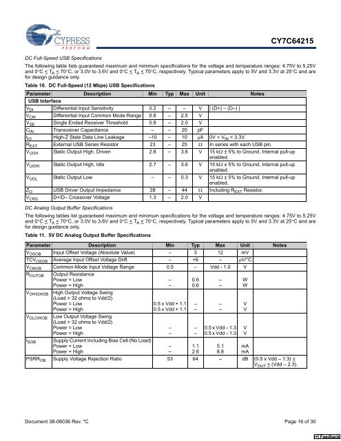
<strong>CY7C64215</strong>DC Full-Speed <strong>USB</strong> SpecificationsThe following table lists guaranteed maximum and minimum specifications for the voltage and temperature ranges: 4.75V to 5.25Vand 0°C < T A < 70°C, or 3.0V to 3.6V and 0°C < T A < 70°C, respectively. Typical parameters apply to 5V and 3.3V at 25°C and arefor design guidance only.Table 10. DC Full-Speed (12 Mbps) <strong>USB</strong> SpecificationsParameter Description Min Typ Max Unit Notes<strong>USB</strong> InterfaceV DI Differential Input Sensitivity 0.2 – – V | (D+) – (D–) |V CM Differential Input Common Mode Range 0.8 – 2.5 VV SE Single Ended Receiver Threshold 0.8 – 2.0 VC IN Transceiver Capacitance – – 20 pFI IO High-Z State Data Line Leakage –10 – 10 μA 0V < V IN < 3.3V.R EXT External <strong>USB</strong> Series Resistor 23 – 25 Ω In series with each <strong>USB</strong> pin.V UOH Static Output High, Driven 2.8 – 3.6 V 15 kΩ ± 5% to Ground. Internal pull-upenabled.V UOHI Static Output High, Idle 2.7 – 3.6 V 15 kΩ ± 5% to Ground. Internal pull-upenabled.V UOL Static Output Low – – 0.3 V 15 kΩ ± 5% to Ground. Internal pull-upenabled.Z O <strong>USB</strong> Driver Output Impedance 28 – 44 Ω <strong>Inc</strong>luding R EXT Resistor.V CRS D+/D– Crossover Voltage 1.3 – 2.0 VDC Analog Output Buffer SpecificationsThe following tables list guaranteed maximum and minimum specifications for the voltage and temperature ranges: 4.75V to 5.25Vand 0°C < T A < 70°C, or 3.0V to 3.6V and 0°C < T A < 70°C, respectively. Typical parameters apply to 5V and 3.3V at 25°C and arefor design guidance only.Table 11. 5V DC Analog Output Buffer SpecificationsParameter Description Min Typ Max Unit NotesV OSOB Input Offset Voltage (Absolute Value) – 3 12 mVTCV OSOB Average Input Offset Voltage Drift – +6 – μV/°CV CMOB Common-Mode Input Voltage Range 0.5 – Vdd - 1.0 VR OUTOBV OHIGHOBV OLOWOBI SOBOutput ResistancePower = LowPower = HighHigh Output Voltage Swing(Load = 32 ohms to Vdd/2)Power = LowPower = HighLow Output Voltage Swing(Load = 32 ohms to Vdd/2)Power = LowPower = HighSupply Current <strong>Inc</strong>luding Bias Cell (No Load)Power = LowPower = High––0.60.60.5 x Vdd + 1.1 –0.5 x Vdd + 1.1 –––––––––WWVV0.5 x Vdd – 1.3 V0.5 x Vdd – 1.3 VPSRR OB Supply Voltage Rejection Ratio 53 64 – dB (0.5 x Vdd – 1.3)