CY7C64215 USB HS DataSheet - Delcom Products Inc.
CY7C64215 USB HS DataSheet - Delcom Products Inc.
CY7C64215 USB HS DataSheet - Delcom Products Inc.
- No tags were found...

You also want an ePaper? Increase the reach of your titles
YUMPU automatically turns print PDFs into web optimized ePapers that Google loves.
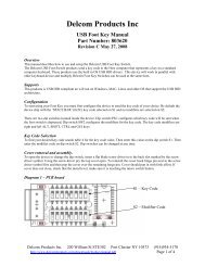
<strong>CY7C64215</strong>Applications■ PC HID devices❐ Mouse (Optomechanical, Optical, Trackball)❐ Keyboards❐ Joysticks■ Gaming❐ Game Pads❐ Console Keyboards■ General Purpose❐ Barcode Scanners❐ POS Terminal❐ Consumer Electronics❐ Toys❐ Remote Controls❐ <strong>USB</strong> to SerialenCoRe III Functional OverviewThe enCoRe III is based on flexible PSoC architecture and is afull-featured, full-speed (12 Mbps) <strong>USB</strong> part. Configurableanalog, digital, and interconnect circuitry enable a high level ofintegration in a host of consumer, and communication applications.This architecture allows the user to create customized peripheralconfigurations that match the requirements of each individualapplication. Additionally, a fast CPU, Flash program memory,SRAM data memory, and configurable IO are included in both28-pin SSOP and 56-pin QFN packages.The enCoRe III architecture, as illustrated in Figure , iscomprised of four main areas: enCoRe III Core, Digital System,Analog System, and System Resources including a full-speed<strong>USB</strong> port. Configurable global busing allows all the deviceresources to combine into a complete custom system. TheenCoRe III <strong>CY7C64215</strong> can have up to seven IO ports thatconnect to the global digital and analog interconnects, providingaccess to 4 digital blocks and 6 analog blocks.enCoRe III CoreThe enCoRe III Core is a powerful engine that supports a richfeature set. The core includes a CPU, memory, clocks, andconfigurable GPIO (General Purpose IO).The M8C CPU core is a powerful processor with speeds up to 24MHz, providing a four MIPS 8-bit Harvard architecture microprocessor.The CPU utilizes an interrupt controller with up to 20vectors, to simplify programming of real-time embedded events.Program execution is timed and protected using the includedSleep and Watch Dog Timers (WDT).Memory encompasses 16K of Flash for program storage, 1K ofSRAM for data storage, and up to 2K of EEPROM emulatedusing the Flash. Program Flash utilizes four protection levels onblocks of 64 bytes, allowing customized software IP protection.enCoRe III incorporates flexible internal clock generators,including a 24 MHz IMO (internal main oscillator) accurate to 8%over temperature and voltage. The 24 MHz IMO is doubled to 48MHz for use by the digital system, if needed. The 48 MHz clockis required to clock the <strong>USB</strong> block and must be enabled for <strong>USB</strong>communication. A low power 32 kHz ILO (internal low speedoscillator) is provided for the Sleep timer and WDT. The clocks,together with programmable clock dividers (as a SystemResource), provide the flexibility to integrate almost any timingrequirement into the enCoRe III. In <strong>USB</strong> systems, the IMOself-tunes to ±0.25% accuracy for <strong>USB</strong> communication.enCoRe III GPIOs provide connection to the CPU, digital andanalog resources of the device. Each pin’s drive mode may beselected from eight options, allowing great flexibility in externalinterfacing. Every pin also has the capability to generate asystem interrupt on high level, low level, and change from lastread.The Digital SystemThe Digital System is composed of four digital enCoRe III blocks.Each block is an 8-bit resource that is used alone or combinedwith other blocks to form 8, 16, 24, and 32-bit peripherals, whichare called user module references.Figure 1. Digital System Block Diagram8Port 7Digital configurations that can be built from the blocks includethose listed below.■ PWMs, Timers and Counters (8-bit and 16-bit)■ UART 8-bit with selectable parity■ SPI master and slave■ I 2 C MasterDigital ClocksFrom CoreRow InputConfigurationPort 5To System BusDIGITAL SYSTEMDigital enCoRe III Block Array8 Row 0DBB00 DBB01 DCB02 DCB034GIE[7:0]GIO[7:0]Port 4Port 3Global DigitalInterconnectPort 2Port 1To AnalogSystemRow OutputConfiguration■ RF Interface: Interface to Cypress CYFI RadioThe digital blocks is connected to any GPIO through a series ofglobal buses that can route any signal to any pin. The buses alsoallow for signal multiplexing and for performing logic operations.This configurability frees your designs from the constraints of afixed peripheral controller.4GOE[7:0]GOO[7:0]Port 088Document 38-08036 Rev. *C Page 2 of 30[+] Feedback