- Page 2 and 3: MITSUBISHIOPTOELECTRONICSOPTICAL SE
- Page 4: OPTICAL SEMICONDUCTORS COMPONENTS G
- Page 7: MITSUBISHI OPTICAL SEMICONDUCTORSCO
- Page 12 and 13: MITSUBISHI OPTICAL SEMICONDUCTORSOR
- Page 14 and 15: MITSUBISHI OPTICAL SEMICONDUCTORSAP
- Page 16 and 17: MITSUBISHI OPTICAL SEMICON.DUCTORSI
- Page 18 and 19: MITSUBISHI OPTICAL SEMICONDUCTORSIN
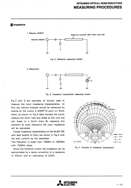
- Page 20 and 21: MITSUBISHI OPTICAL SEMICONDUCTORSIN
- Page 22 and 23: MITSUBISHI OPTICAL SEMICONDUCTORSPR
- Page 24 and 25: MITSUBISHI OPTICAL SEMICONDUCTORSTE
- Page 26 and 27: MITSUBISHI OPTICAL SEMICONDUCTORSTE
- Page 28 and 29: MITSUBISHI OPTICAL SEMICONDUCTORSME
- Page 32 and 33: MITSUBISHI OPTICAL SEMICONDUCTORSME
- Page 34 and 35: MITSUBISHI OPTICAL SEMICONDUCTORSME
- Page 36 and 37: MITSUBISHI OPTICAL SEMICONDUCTORSME
- Page 38 and 39: MITSUBISHI OPTICAL SEMICONDUCTORSME
- Page 40 and 41: MITSUBISHI OPTICAL SEMICONDUCTORSME
- Page 42 and 43: MITSUBISHI OPTICAL SEMICONDUCTORSME
- Page 44 and 45: MITSUBISHI OPTICAL SEMICONDUCTORSDR
- Page 46 and 47: MITSUBISHI OPTICAL SEMICONDUCTORSRE
- Page 48: MITSUBISHI OPTICAL SEMICONDUCTORSSA
- Page 52 and 53: MITSUBISHI LASER DIODESML2XX1 SERIE
- Page 54 and 55: MITSUBISHI LASER DIODESML2XX1 SERIE
- Page 56 and 57: MITSUBISHI LASER DIODESML2XX1 SERIE
- Page 58 and 59: ML2XX1 SERIESFOR OPTICAL COMMUNICAT
- Page 60 and 61: MITSUBISHI LASER DIODESML3XX1 SERIE
- Page 62 and 63: MITSUBISHI LASER DIODESML3XX1 SERIE
- Page 64 and 65: MITSUBISHI LASER DIODESML3XX1 SERIE
- Page 66 and 67: MITSUBISHI LASER DIODESML4XX2 SERIE
- Page 68 and 69: MITSUBISHI LASER DIODESML4XX2 SERIE
- Page 70 and 71: MITSUBISHI LASER DIODESML4XX2 SERIE
- Page 72 and 73: MITSUBISHI LASER DIODESML4XX2 SERIE
- Page 74 and 75: MITSUBISHI LASER DIODESML4XX2A SERI
- Page 76 and 77: MITSUBISHI LASER DIODESML4XX2A SERI
- Page 78 and 79: MITSUBISHI LASER DIODESML4XX2A SERI
- Page 80 and 81:
MITSUBISHI LASER DIODESML4XX2A SERI
- Page 82 and 83:
MITSUBISHI LASER DIODESML4XX3 SERIE
- Page 84 and 85:
MITSUBISHI LASER DIODESML4XX3 SERIE
- Page 86 and 87:
MITSUBISHI LASER DIODESML4XX3 SERIE
- Page 88 and 89:
MITSUBISHI LASER DIODESML4XX5 SERIE
- Page 90 and 91:
MITSUBISHI LASER DIODESML4XX5 SERIE
- Page 92 and 93:
MITSUBISHI LASER DIODESML4XX5 SERIE
- Page 94 and 95:
MITSUBISHI LASER DIODESML4XX10 SERI
- Page 96 and 97:
MITSUBISHI LASER DIODESML4XX10 SERI
- Page 98 and 99:
MITSUBISHI LASER DIODESML4XX10 SERI
- Page 100 and 101:
MITSUBISHI LASER DIODESML4XX14 SERI
- Page 102 and 103:
MITSUBISHI LASER DIODESML4XX14 SERI
- Page 104 and 105:
MITSUBISHI LASER DIODESML4XX14 SERI
- Page 106 and 107:
MITSUBISHI LASER DIODESML4XX14 SERI
- Page 108 and 109:
MITSUBISHI LASER DIODESML4XX15 SERI
- Page 110 and 111:
MITSUBISHI LASER DIODESML4XX15 SERI
- Page 112 and 113:
MITSUBISHI LASER DIODESML4XX15 SERI
- Page 114 and 115:
~MITSUBISHI LASER DIODESML4XX16 SER
- Page 116 and 117:
MITSUBISHI LASER DIODESML4XX16 SERI
- Page 118 and 119:
MITSUBISHI LASER DIODESML4XX16 SERI
- Page 120 and 121:
MITSUBISHI LASER DIODESML4XX19 SERI
- Page 122 and 123:
MITSUBiSHI LASER DIODESML5XX1A SERI
- Page 124 and 125:
MITSUBISHI LASER DIODESML5XX1A SERI
- Page 126 and 127:
MITSUBISHI LASER DIODESML5XX1A SERI
- Page 128 and 129:
MITSUBISHI LASER DIODESML5XX1 A SER
- Page 130 and 131:
MITSUBISHI LASER DIODESML5XX3A SERI
- Page 132 and 133:
MITSUBISHI LASER DIODESML5XX3A SERI
- Page 134 and 135:
MITSUBISHI LASER DIODESML5XX3A SERI
- Page 136 and 137:
MITSUBISHI LASER DIODESML5XX4 SERIE
- Page 138 and 139:
MITSUBISHI LASER DIODESML5XX4 SERIE
- Page 140 and 141:
MITSUBISHI LASER DIODESML5XX4 SERIE
- Page 142 and 143:
MITSUBISHI LASER DIODESML5XX5 SERIE
- Page 144 and 145:
MITSUBISHI LASER DIODESML5XX5 SERIE
- Page 146 and 147:
MITSUBISHI LASER DIODESML5XX5 SERIE
- Page 148 and 149:
MITSUBISHI LASER DIODESML5XX5 SERIE
- Page 150 and 151:
MITUBISHI LASER DIODESML6XX1A SERIE
- Page 152 and 153:
MITSUBISHI LASER DIODESML6XX1A SERI
- Page 154 and 155:
, Mil ~U"I;'"I ~;'I:.n ..,."'.., ..
- Page 156 and 157:
MITSUBISHI LASER DIODESML6XX1A SERI
- Page 158 and 159:
MITSUBISHI LASER DIODESML6XX3A SERI
- Page 160 and 161:
MITSUBISHI LASER DIODESML6XX3A SERI
- Page 162 and 163:
MITSUBISHI LASER DIODESML6XX3A SERI
- Page 164 and 165:
MITSUBISHI LASER DIODESML6XX10 SERI
- Page 166 and 167:
MITSUBISHI LASER DIODESML6XX10 SERI
- Page 168 and 169:
MITSUBISHI LASER DIODESML6XX10 SERI
- Page 170 and 171:
MITSUBISHI LASER DIODESMl6XX11 SERI
- Page 172 and 173:
MITSUBISHI LASER DIODESML6XX11 SERI
- Page 174 and 175:
MITSUBISHI LASER DIODESML6XX11 SERI
- Page 176 and 177:
MITSUBISHI LASER DIODESML6XX11 SERI
- Page 178 and 179:
MITSUBISHI LASER DIODESML6XX14 SERI
- Page 180 and 181:
MITSUBISHI LASER DIODEML7XX1 SERIES
- Page 182 and 183:
MITSUBISHI LASER DIODEML7XX1 SERIES
- Page 184 and 185:
MITSUBISHI LASER DIODEML7XX1 SERIES
- Page 186 and 187:
MITSUBISHI LASER DIODEML7XX1 SERIES
- Page 188 and 189:
MITSUBISHI LASER DIODESML7XX1A SERI
- Page 190 and 191:
MITSUBISHI LASER DIODESML7XX1A SERI
- Page 192 and 193:
MITSUBISHI LASER DIODESML7XX2 SERIE
- Page 194 and 195:
MITSUBISHI LASER DIODESML7XX2 SERIE
- Page 196 and 197:
MITSUBISHI LASER DIODESML7XX2 SERIE
- Page 198 and 199:
MITSUBISHI LASER DIODESML7XX3 SERIE
- Page 200 and 201:
MITSUBISHII,.ASER DIODESML7XX3 SERI
- Page 202 and 203:
MITSUBISHI LASER DIODESML7XX5 SERIE
- Page 204 and 205:
~MITSUBISHI LASER DIODESML8XX1 SERI
- Page 206 and 207:
MITSUBISHI LA51:FI DIUUt:.~ML8XX1 S
- Page 208 and 209:
MITSUBISHI LASER DIODESML8XX1 SERIE
- Page 210 and 211:
MITSUBISHI,LASER DIODESML9XX1 SERIE
- Page 212 and 213:
MITSUBISHI LASER DIODESML9XX1 SERIE
- Page 214 and 215:
MIT$UBISHI LASER DIODESML9XX1 SERIE
- Page 216 and 217:
MITSUBISHI LASER DIODESML9XX1A SERI
- Page 218 and 219:
MITSUBISHI LASER DIODESML9XX1A SERI
- Page 220 and 221:
MITSUBISHI LASER DIODESML9XX2 SERIE
- Page 222 and 223:
MITSUBISHI LASER DIODESML9XX2 SERIE
- Page 224 and 225:
.~MITSUBISHI LASER DIODESML9XX2 SER
- Page 228 and 229:
MITSUBISHI LASER DIODESML9XX3 SERIE
- Page 230:
MITSUBISHI LASER DIODESML9XX5 SERIE
- Page 234 and 235:
HIGH RADIANCE LIGHT EMITTING DIODES
- Page 236 and 237:
HIGH RADIANCE LIGHT EMITTING DIODES
- Page 240:
HIGH RADIANCE LIGHT EMmlNG DIODESME
- Page 243 and 244:
HIGH RADIANCE LIGHT EMITTING DIODES
- Page 245 and 246:
HIGH RADIANCE LIGHT EMITTING DIODES
- Page 248:
PHOTODIODES
- Page 252 and 253:
MITSUBISHI SILI(;UN AVALAN\,;Mt: t"
- Page 254 and 255:
MITSUBISHI SILICON AVALANCHE PHOTOD
- Page 256 and 257:
MITSUBISHI SILICON AVALANCHE PHOTOD
- Page 258 and 259:
MITSUBISHI SILICON AVALANCHE PHOTOD
- Page 260 and 261:
MITSUBISHllnGaAs PHOTODIODESPD7XX5
- Page 262 and 263:
MITSUBISHllnGaAs PHOTODIODESPD7XX5.
- Page 264 and 265:
MITSUBISHllnGaAs PHOTODIODESPD7XX6
- Page 266 and 267:
MITSUBISHllnGaAs PHOTODIODESPD7XX6
- Page 268 and 269:
MITSUBISHllnGaAs PHOTODIODESPD7XX7
- Page 270 and 271:
MITSUBISHllnGaAs PHOTODIODESPD7XX7
- Page 272 and 273:
MITSUBISHllnGaAs PHOTODIODESPD8XX2
- Page 274:
MITSUBISHllnGaAs PHOTODIODESPD8XX2
- Page 278:
MITSUBISHI OPTICAL SEMICONDUCTORSPR
- Page 282 and 283:
LIST OF PRODUCTSLD Module for Singl
- Page 284 and 285:
LIST OF PRODUCTSDlgltal·Optlcal Tr
- Page 286 and 287:
PRODUCT DESIGNATION CODEPRODUCT DES
- Page 288 and 289:
MEASURING PROCEDURESFOR OPTOELECTRO
- Page 290:
OPTICAL-FIBER COMPONENTS OAT A SHEE
- Page 293 and 294:
FU~011 SLD-N20.781..1 m Connectorlz
- Page 295 and 296:
FU-16SLD-N1, FU-17SLD-N11.311 m Con
- Page 297 and 298:
FU-16SLD-N3, FU-17SLD-N31.31..1 m C
- Page 299 and 300:
FU-16SLD-N3, FU-17SLD-N31.31l m Con
- Page 301 and 302:
FU-411SLD1.31..l m LD Module with S
- Page 303 and 304:
FU-411 SLO-201 .. 3 ~ m LD Module w
- Page 305 and 306:
FU-611SLD1.55 iJ. m LD Module with
- Page 307 and 308:
FU-611SLD1.55 Il m LD Module with S
- Page 309 and 310:
FU-611 SLD-151.55 Il m LD Module wi
- Page 311 and 312:
FU-43SLD-11.3 1..1 m LD Module with
- Page 313 and 314:
1FU-43SLD-21,31.1 m LD Module with
- Page 315 and 316:
FU-43SLD-21.31.1 m LD Module with S
- Page 317 and 318:
FU-44SLD-11.3 1.1 m LD Module with
- Page 319 and 320:
FU-44SLD-71.31..l m LD Module with
- Page 321 and 322:
FU-44SLD-71.3 iJ m LD Module with S
- Page 323 and 324:
FU-45SLD1.31-1 m LD Module with Sin
- Page 325 and 326:
FU-64SLD-11.551..l m LD Module with
- Page 327 and 328:
FU-64SLD-11.55 1..1 m LD Module wit
- Page 329 and 330:
FU-64SLD-71.55 IJ m LD Module with
- Page 331 and 332:
FU-41SDF, FU-44SDF1.31..1 m DFB-LD
- Page 333 and 334:
FU-41 SDF, FU-44SDF1.31J m DFB-LD M
- Page 335 and 336:
FU-45SDF-38(CATV Application)1.3 J.
- Page 337 and 338:
FU-45SDF-4(Digital Application)1,31
- Page 339 and 340:
FU-45SDF-4(Digital"Application)1.31
- Page 341 and 342:
FU-48SDF-1(for 2.5Gbps Digital Appl
- Page 343 and 344:
FU-61 SDF ,FU-64SDF1.551-1 m DFB-LD
- Page 345 and 346:
FU-61 SDF,FU-64SDF1.551..1 m DFB-LD
- Page 347 and 348:
FU-65SDF-3(Analog ApplicatiOn)1.551
- Page 349 and 350:
FU-65SDF-41.55 tJ. m DFB-LD Module
- Page 351 and 352:
FU-65SDF~41.551..l m DFB-LD Module
- Page 353 and 354:
FU-68SDF-2DFB-LD Module with Single
- Page 355 and 356:
FU-01 LD-N (O.78),FU-27LD{O.78)O.78
- Page 357 and 358:
FU-01 LD-N (O.78),FU-27LD{O.78)0;78
- Page 359 and 360:
FU-01 LD~N{O.85), FU-27LD (O.85)0.8
- Page 361 and 362:
FU-23LD0.85 1.1 m LD Module with Mu
- Page 363 and 364:
FU-23LD0.851.1 m LD Module with Mul
- Page 365 and 366:
FU-11LD-N1.31J m Connectorlzed LD M
- Page 367 and 368:
FU-33LD1.3 iJIt1 LD Module with Mul
- Page 369 and 370:
FU-02LE-N,FU-23LE0.851-1 m LED Modu
- Page 371 and 372:
FU-02LE-N, FU-23LE0.8511 m LED Modu
- Page 373 and 374:
FU-13LE-N,FU-34LE1.31..1 m LED Modu
- Page 375 and 376:
FU-04PO-N, FU-21 POPO Module for Sh
- Page 377 and 378:
FU-04PO-N, FU-21 POPO Module for Sh
- Page 379 and 380:
0.65FU-15PD-N, FU-16PD-NPO Module f
- Page 381 and 382:
FU-35PDPO Module for Long Wavelengt
- Page 383 and 384:
FU-05AP-N, FU-25APAPD Module for Sh
- Page 385 and 386:
FU-05AP-N, FU-25APAPD Module for Sh
- Page 387 and 388:
FU-12AP-N, FU-32APAPD Module for Lo
- Page 389 and 390:
FU-13AP-NAPD Module for Long Wavele
- Page 391 and 392:
FU-310APAPO Module for Long Wavelel
- Page 393 and 394:
FU-310APAPD Module for Long Wavelen
- Page 395 and 396:
MF-12SDS-TR113-006Digital Optical T
- Page 397 and 398:
MF-156DS-TR124-002/003Dlgltal Optic
- Page 399 and 400:
M:F-156DS-TR124-002/003Digital Opti
- Page 401 and 402:
MF-622DF-T12-007 -011Optical Transm
- Page 403 and 404:
~8~~MF-622DF-T12-007-011Optical Tra
- Page 405 and 406:
MF-622DS-R13-002/R14-002,003Optical
- Page 407 and 408:
MF-20DF-TR014-002Digital Optical Tr
- Page 409 and 410:
MF-32DF-T01/R03Digital Optical Tran
- Page 411 and 412:
; FC~01PN-SMF, FC-01 PN-PC-SMF,FC-D
- Page 413 and 414:
FC-01 PN, FC-01 PN-PC, FC-01 PN-SPC
- Page 415 and 416:
MITSUBISHI OPTOELECTRONICSOPTICAL S