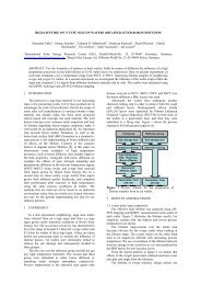
large area and screen printed n-type silicon solar cells - ISC Konstanz
large area and screen printed n-type silicon solar cells - ISC Konstanz
large area and screen printed n-type silicon solar cells - ISC Konstanz

Create successful ePaper yourself
Turn your PDF publications into a flip-book with our unique Google optimized e-Paper software.
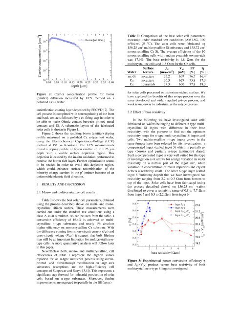
Table I: Comparison of the best <strong>solar</strong> cell parametersmeasured under st<strong>and</strong>ard test conditions (AM1.5G, 100mW/cm 2 , 25 o C). The <strong>solar</strong> <strong>cells</strong> were fabricated on156.25 cm 2 multicrystalline Si substrates <strong>and</strong> 155.72 cm 2monocrystalline Cz Si. The average efficiency of the 10monocrystalline <strong>cells</strong> with r<strong>and</strong>om pyramids texture etchwas 17.9%. The base resistivity is 1.8 Ωcm for themulticrystalline <strong>cells</strong> <strong>and</strong> 1.5 Ωcm for the Cz <strong>cells</strong>.WaferSurfacetextureJ sc[mA/cm 2 ]V oc[mV]FF[%]η[%]mc-Si isotexture 35.2 607 76.7 16.4Cz isotexture 36.3 629 75.8 17.3Cz r.pyramids 37.3 630 77.8 18.3Figure 2: Carrier concentration profile for boron(emitter) diffusion measured by ECV method on apolished Cz Si wafer.antireflection coating layer deposited by PECVD [7]. Thecell process is completed with <strong>screen</strong> printing of the front<strong>and</strong> back contacts followed by a co-firing step in order tobe able to make Ohmic contact between <strong>printed</strong> metalcontacts <strong>and</strong> Si. A schematic layout of the fabricated<strong>solar</strong> <strong>cells</strong> is shown in Figure 1.Figure 2 shows the resulting boron (emitter) dopingprofile measured on a polished Cz n-<strong>type</strong> test wafer,using the Electrochemical Capacitance-Voltage (ECV)method at <strong>ISC</strong> in <strong>Konstanz</strong>. The ECV measurementsreveal a doping profile of boron emitter up to 0.25 µmdepth with a visible surface depletion region. Thisdepletion is caused by the in-situ oxidation performed toremove the boron rich layer. Further optimization seemsto be needed in order to avoid this depletion region,which could enhance surface recombination of theminority charge carriers in the p + emitter because of anunfavorable electric field direction.3 RESULTS AND D<strong>ISC</strong>USSION3.1 Mono- <strong>and</strong> multi-crystalline cell resultsTable I shows the best <strong>solar</strong> cell parameters, obtainedusing the process described above, on multi- <strong>and</strong> monocrystalline<strong>silicon</strong> wafers. These measurements werecarried out under the st<strong>and</strong>ard test conditions using aclass A <strong>solar</strong> simulator. As can be seen from the table, aconversion efficiency of 16.4% is achieved on multicrystallinen-<strong>type</strong> substrates <strong>and</strong> nearly 1% absolutehigher efficiency on monocrystalline Cz substrate. Withthe difference coming from short-circuit current (J SC ) <strong>and</strong>open-circuit voltage (V OC ) it suggest that bulk lifetimemay still be an important limitation for multicrystalline n-<strong>type</strong> <strong>cells</strong>. A more quantitative analysis will follow laterin this paper.Nevertheless both, mono- <strong>and</strong> multicrystalline, cellefficiencies of table I represent the highest valuesreported for an n-<strong>type</strong> industrial process using <strong>screen</strong><strong>printed</strong><strong>and</strong> fired-through metallization on <strong>large</strong> <strong>area</strong>substrates (exceptions are the high-efficiency cellconcepts of Sunpower <strong>and</strong> Sanyo [3,4]). This represents asignificant step forward for industrial production of <strong>solar</strong><strong>cells</strong> based on n-<strong>type</strong> substrates. Moreover, furtherimprovements are expected (especially in the fill factor)for <strong>solar</strong> <strong>cells</strong> processed on isotexture etched surface. Wehave explored the benefits of this n-<strong>type</strong> process over themore developed <strong>and</strong> widely applied p-<strong>type</strong> process, <strong>and</strong>work is underway to industrialize the n-<strong>type</strong> process.3.2 Effect of base resistivityIn the following we have investigated <strong>solar</strong> <strong>cells</strong>fabricated on wafers belonging to different n-<strong>type</strong> multicrystallineSi ingots with difference in their baseresistivity, with the purpose to find out the optimumresistivity range for n-<strong>type</strong> multi-crystalline Si ingots <strong>and</strong><strong>cells</strong>. Two multicrystalline n-<strong>type</strong> ingots grown in thesame furnace have been selected for this investigation: acompensated ingot (called ingot 5) which is partially p-<strong>type</strong> (boron) <strong>and</strong> partially n-<strong>type</strong> (antimony) doped.Such a compensated ingot is very well suited for this <strong>type</strong>of investigation as it allows for a <strong>large</strong> variation in waferresistivity on a narrow part of the ingot size, whilevariation in concentration of metal impurities <strong>and</strong> crystaldefects is relatively small. The other n-<strong>type</strong> ingot (calledingot 6 /antimony doped) that we have investigated hasresistivity ranging from 2.2 to 0.3 Ωcm from bottom totop of the ingot. Solar <strong>cells</strong> have been fabricated (usingthe process described above) on 156.25 cm 2 wafersdistributed to cover a resistivity range of 0.8 to 7.7 Ωcmfrom ingot 5 <strong>and</strong> 0.3 to 2.2 Ωcm from ingot 6.Figure 3: Experimental power conversion efficiency η<strong>and</strong> J SC ×V OC product versus base resistivity of bothmulticrystalline n-<strong>type</strong> Si ingots investigated.