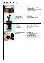
large area and screen printed n-type silicon solar cells - ISC Konstanz
large area and screen printed n-type silicon solar cells - ISC Konstanz
large area and screen printed n-type silicon solar cells - ISC Konstanz

You also want an ePaper? Increase the reach of your titles
YUMPU automatically turns print PDFs into web optimized ePapers that Google loves.
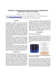
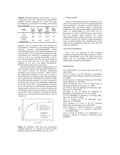
Table II: PC1D fit parameters used in figure 5. L d,emitteris taken at N A =10 20 cm −3 , whereas ∆V OC represents thedifference between calculated V OC , when only Augerrecombination is considered in the emitter, <strong>and</strong> measuredV OC of the <strong>cells</strong>.Waferequiv.L d,bulk L d,emitter∆VFe OC[µm] [µm]i[cm −3 [mV]]Cz 841 0.56 9×10 14 6mc-Si(reference)284 0.47 2×10 15 14mc-Si(50 ppmw Fe)192 0.41 4×10 15 22impurities may be present. Thus, the interstitial Feconcentration is used here as a convenient parameter torepresent increased Schockly-Read-Hall emitterrecombination in general. The resulting fit parameters areshown in table II. It was found that consideration of thiscontamination was essential to simultaneously fit IQEcurves as well as V OC correctly . Incidentally, it can beseen that the 50 ppmw of Fe have only modest effect onL d,bulk of the <strong>solar</strong> <strong>cells</strong> but it can bring significantlimitation to V OC due to the emitter contamination.Further analysis of this effect is in progress.Based on fitted IQE of different multicrystalline <strong>and</strong>monocrystalline <strong>cells</strong> <strong>and</strong> using our model calculation wewere able to identify the efficiency enhancementpossibility for our n-<strong>type</strong> cell process. Figure 6 showsthe experimental efficiencies of the <strong>cells</strong> of figure 5.These efficiencies are plotted together with the calculatedcurve against the ratio of minority carrier diffusion lengthin the bulk <strong>and</strong> wafer thickness (L d,bulk /W), assuming anisotexture etched surface, same metallization shadowing,FF, <strong>and</strong> W, for all <strong>cells</strong>. A good agreement is observedfor all <strong>cells</strong> allowing us to quantify the relation betweenmaterial quality (given by L d,bulk ) <strong>and</strong> the resulting <strong>solar</strong>cell efficiency when all other parameters of the processare the same. Work is underway to elucidate the relationbetween L d,bulk <strong>and</strong> the presence of some defects in mc-Siwafers [11].4 CONCLUSSIONWe have demonstrated a process to fabricate n-<strong>type</strong><strong>solar</strong> <strong>cells</strong> on <strong>large</strong> <strong>area</strong> (156.25 cm 2 ) multicrystalline <strong>and</strong>mono-crystalline Cz substrates, involving diffusion ofphosphorus BSF <strong>and</strong> boron emitter, <strong>screen</strong>-<strong>printed</strong>metallization <strong>and</strong> firing through, leading to efficiencies of16.4% on multicrystalline Si <strong>and</strong> 18.3% on Cz.Experiments on wafers of different base resistivity showthat the optimum target resistivity for n-<strong>type</strong>multicrystalline <strong>silicon</strong> wafers lies between 1.5 to 4 Ωcmin order to maximize the efficiency output thorough theingot. In multicrystalline <strong>cells</strong>, modeling gives a clearindication that contaminants inside the wafer affect theemitter recombination.ACKNOWLEDGEMENTSThis work was supported by the EuropeanCommission within the FoXy project under the contractnumber 019811(SES6), <strong>and</strong> by the Dutch agency forenergy <strong>and</strong> the environment SenterNovem. ECNacknowledges cooperation with Tempress.REFERENCES[1] D. MacDonald, L. J. Geerligs, Appl. Phys. Lett. 85,4061 (2004).[2] J. E. Cotter et. al., 15 th Workshop on CrystallineSilicon Solar Cells & Modules: Materials <strong>and</strong> Processes,p. 3 (2005).[3] M. Taguchi, A. Terakawa, E. Maruyama, M. Tanaka,Progr. Photovolt. 13, 481 (2005)[4] K. R. McIntosh, Proc. of the 3 rd World Conf. onPhotovoltaic Energy Conversion, p. 971 (2003).[5] Asuha, S. Imai, M. Takahashi, H. Kobayashi, Appl.Phys. Lett. 85, 3783 (2004).[6] Asuha, Y. Liu, O. Maida, M. Takahashi, H.Kobayashi, J. Electrochem. Soc. 151, 824 (2004).[7] V. D. Mihailetchi, Y. Komatsu, L. J. Geerligs, Appl.Phys. Lett. 92, 063510 (2008).[8] L. J. Geerligs <strong>and</strong> D. H. Macdonald, Progr.Photovolt. 12, 309 (2004).[9] J. Schmidt et al., Proc. of the 22 nd EuropeanPhotovoltaic Solar Energy Conf., p. 998 (2007).[10] A. Bentzen, A. Holt, R. Kopecek, G. Stokkan,J. S. Christensen, B. G. Svensson, J. Appl. Phys.99, 093509 (2006).[11] G. Coletti, R. Kv<strong>and</strong>e, V. D. Mihailetchi, L. J.Geerligs, L. Arnberg, E. J. Øvrelid, J. Appl. Phys. (to bepublished).Figure 6: Calculated (solid line) <strong>and</strong> experimental(symbols) efficiency as a function of minority carrierdiffusion length <strong>and</strong> wafer thickness ratio (L d,bulk /W).