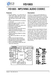
4 Packages and Pin Descriptions<strong>VS1000</strong>4 PACKAGES AND PIN DESCRIPTIONS4.1 PackagesLPQFP-48 is lead (Pb) free and RoHS-compliant package. RoHS is a short name of Directive2002/95/EC on the restriction of the use of certain hazardous substances in electrical andelectronic equipment.148Figure 1: <strong>VS1000</strong> pin configuration, LQFP-48.LQFP-48 package dimensions are at http://www.vlsi.fi/ .Figure 2: <strong>VS1000</strong> pins, LQFP-48.Version: 1.43, 2013-05-28 10
<strong>VS1000</strong>4 PACKAGES AND PIN DESCRIPTIONS4.2 LQFP-48 Pin DescriptionsPin NameLQFPPinPinTypeFunctionXRESET 1 DI Active low asynchronous reset, schmitt-trigger inputNFDIO0 / GPIO0_0 2 DIO Nand-flash IO0 / General-purpose IO Port 0, bit 0NFDIO1 / GPIO0_1 3 DIO Nand-flash IO1 / General-purpose IO Port 0, bit 1NFDIO2 / GPIO0_2 4 DIO Nand-flash IO2 / General-purpose IO Port 0, bit 2NFDIO3 / GPIO0_3 5 DIO Nand-flash IO3 / General-purpose IO Port 0, bit 3DGND0 6 DGND Core & I/O groundIOVDD1 7 IOPWR I/O power supplyTEST 8 DI Test mode input (active high), connect to DGNDNFDIO4 / GPIO0_4 9 DIO Nand-flash IO4 / General-purpose IO Port 0, bit 4NFDIO5 / GPIO0_5 10 DIO Nand-flash IO5 / General-purpose IO Port 0, bit 5NFDIO6 / GPIO0_6 11 DIO Nand-flash IO6 / General-purpose IO Port 0, bit 6NFDIO7 / GPIO0_7 12 DIO Nand-flash IO7 / General-purpose IO Port 0, bit 7NFRDY / GPIO0_8 13 DIO Nand-flash READY / General-purpose IO Port 0, bit 8NFRD / GPIO0_9 14 DIO Nand-flash RD / General-purpose IO Port 0, bit 9NFCE / GPIO0_10 15 DIO Nand-flash CE / General-purpose IO Port 0, bit 10NFCLE / GPIO0_12 16 DIO Nand-flash CLE / General-purpose IO Port 0, bit 12NFALE / GPIO0_13 17 DIO Nand-flash ALE / General-purpose IO Port 0, bit 13DGND1 18 DGND Core & I/O groundIOVDD2 19 IOPWR I/O power supplyNFWR / GPIO0_11 20 DIO Nand-flash WR / General-purpose IO Port 0, bit 11CS2 / GPIO0_14 21 DIO General-purpose IO Port 0, bit 14XCS / GPIO1_0 22 DIO SPI XCS / General-Purpose I/O Port 1, bit 0SCLK / GPIO1_1 23 DIO SPI CLK / General-Purpose I/O Port 1, bit 1SI / GPIO1_2 24 DIO SPI MISO / General-Purpose I/O Port 1, bit 2SO / GPIO1_3 25 DIO SPI MOSI / General-Purpose I/O Port 1, bit 3TX / GPIO1_4 26 DIO UART TX / General-Purpose I/O Port 1, bit 4RX / GPIO1_5 27 DIO UART RX / General-Purpose I/O Port 1, bit 5XTALI 28 AI Crystal inputXTALO 29 AO Crystal outputIOVDD 30 IOPWR I/O power supply, Regulator outputDGND2 31 DGND Core & I/O groundCVDD 32 CPWR Core power supply, Regulator outputVHIGH 33 PWR Power supply, Regulator inputAVDD 34 APWR Analog power supply, Regulator outputUSBP 35 AIO USB differential + in / out, controllable 1.5kΩ pull-upUSBN 36 AIO USB differential - in / outPWRBTN 37 APB / DI Power button for Regulator startup and Power KeyAGND0 38 APWR Analog groundAVDD1 39 APWR Analog power supplyRIGHT 40 AO Right channel outputAGND1 41 APWR Analog groundAGND2 42 APWR Analog groundCBUF 43 AO Common voltage buffer for headphones (1.2V nominal)AVDD2 44 APWR Analog power supplyRCAP 45 AIO Filtering capacitance for referenceAVDD3 46 APWR Analog power supplyLEFT 47 AO Left channel outputAGND3 48 APWR Analog groundVersion: 1.43, 2013-05-28 11