
Create successful ePaper yourself
Turn your PDF publications into a flip-book with our unique Google optimized e-Paper software.
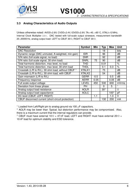
<strong>VS1000</strong>3 CHARACTERISTICS & SPECIFICATIONS3.3 Analog Characteristics of Audio OutputsUnless otherwise noted: AVDD=2.8V, CVDD=2.4V, IOVDD=2.8V, TA=-40..+85 ◦ C, XTALI=12 MHz,Internal Clock Multiplier 3.0×. DAC tested with full-scale output sinewave, measurement bandwidth20..20000 Hz, analog output load: LEFT to CBUF 30 Ω, RIGHT to CBUF 30 Ω.Parameter Symbol Min Typ Max UnitDAC Resolution 18 bitsDynamic range (DAC unmuted, A-weighted, min gain) IDR 96 dBS/N ratio (full scale signal, no load) SNR 92 dBS/N ratio (full scale signal, 30 ohm load) SNRL 75 90 dBTotal harmonic distortion, max level, no load THD 0.01 %Total harmonic distortion, max level, 30 ohm load THDL 0.1 0.3 %Crosstalk (L/R to R/L), 30 ohm load, without CBUF 1 XTALK1 75 dBCrosstalk (L/R to R/L), 30 ohm load, with CBUF XTALK2 54 dBGain mismatch (L/R to R/L) GERR -0.5 0.5 dBFrequency response AERR -0.05 0.05 dBFull scale output voltage LEVEL 450 530 600 mVrmsDeviation from linear phase PH 0 5◦Analog output load resistance AOLR 30 2 ΩAnalog output load capacitance AOLC 100 3 pFDC level (CBUF, LEFT, RIGHT) 1.1 1.3 VCBUF disconnect current (short-circuit protection) 130 200 mA1 Loaded from Left/Right pin to analog ground via 100 µF capacitors.2 AOLR may be lower than Typical, but distortion performance may be compromised. Also,there is a maximum current that the internal regulators can provide.3 CBUF must have external 10 Ω + 47 nF load, LEFT and RIGHT must have external 20 Ω +10 nF load for optimum stability and ESD tolerance.Version: 1.43, 2013-05-28 6