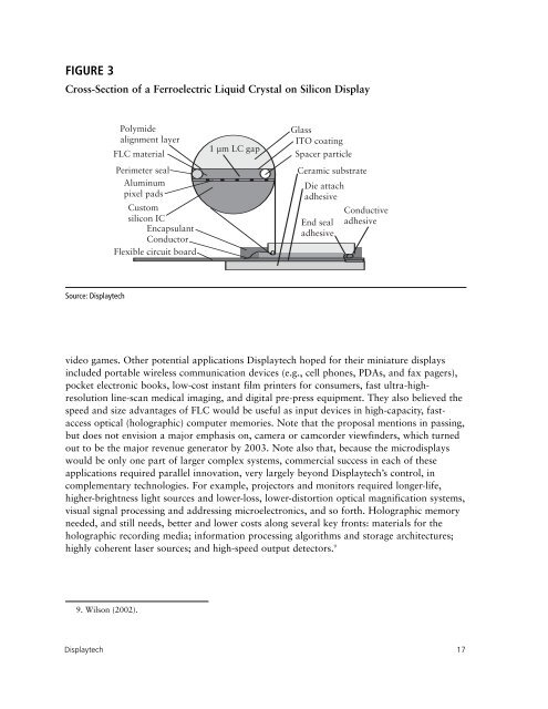
On the manufacturing process side, a major challenge was to reduce manufacturing costs tothe point where commercial applications were economically attractive. The lab-scaleprocesses were labor intensive <strong>and</strong> had quite high failure rates. The proposed process was“wafer-scale,” that is, manufacturing 50 to 100 or more devices on a single silicon wafer,processed as one unit. However, as shown in Figure 3, the displays have glass, which cover agap in the FLC material, enclosed over a silicon integrated circuit (IC). One major problemwas how to scribe or dice both glass <strong>and</strong> silicon in order to separate—“singulate” in industryjargon—the multiple microdisplays on the wafer. Traditional liquid crystal display (LCD)manufacturing involved only scribing glass, <strong>and</strong> traditional microchips involve just silicon.Displaytech wanted to investigate several alternative methods using equipment from variousvendors.Another process focus was improving the edge sealing method for depositing adhesives in thetiny gap between silicon <strong>and</strong> glass, the “perimeter seal” in Figure 3. Technically, to getbistable behavior, the gap needed to be 1 micron, 10 times smaller than in typical liquidcrystal (LC) displays. So, the sealing process needed to deposit far smaller amounts <strong>of</strong>adhesive. Reliably depositing glue for 1-micron spaces, in a repeatable process for high-yield,high-volume manufacturing, turned out to be a significant technical challenge.On the materials side, they hoped to improve the effective lifetime <strong>of</strong> the FLC materials, inpart through composition <strong>and</strong> characterization research to overcome electrolytic degradationproblems <strong>of</strong> FLCs. The bistable property <strong>of</strong> FLC materials eliminates the need to apply DCvoltage constantly. This has commercial advantages in power consumption, for example.However, in the original composition <strong>of</strong> the FLC materials, it was difficult to maintain goodbistability over time <strong>and</strong> wide temperature ranges. Bistable formulations tended to reduceeither switching speed or contrast, both important in commercial applications. Displaytechinvestigated various compounds as components <strong>of</strong> FLC compositions to improve theseproperties. While the complete multi-ingredient FLC composition developed under <strong>ATP</strong>funding is now only used in minor market applications, several <strong>of</strong> the individual compoundsidentified remain in use in Displaytech’s current commercial applications.PROPOSED APPLICATIONSIn the 1994 proposal, Displaytech envisioned selling the microdisplays to a variety <strong>of</strong>markets. The hope was that the small-scale, fast-switching characteristics would not onlydisplace conventional CRT tubes in some display markets, but also enable other marketapplications where CRTs <strong>and</strong> st<strong>and</strong>ard LC displays were less than adequate. The mostattractive markets for displacing CRTs, one <strong>of</strong> the last bastions <strong>of</strong> vacuum tube technology,were in televisions <strong>and</strong> computer monitors. Displaytech believed the FLC microdisplays couldbe combined with light sources <strong>and</strong> optics to make relatively thin, light, yet high-resolutionfront- or rear-projection displays, including high-definition televisions in size ranges up to 60inches <strong>and</strong> <strong>of</strong>fice projectors for computer presentations. They also hoped to enable a majormarket in head-mounted goggles for virtual reality, portable computing, stereo computeraided design (CAD) workstations, medical <strong>and</strong> industrial h<strong>and</strong>s-free visualization, <strong>and</strong> 3D16 DIRECT AND SPILLOVER EFFECTS OF <strong>ATP</strong>-FUNDED PHOTONICS TECHNOLOGIES
FIGURE 3Cross-Section <strong>of</strong> a Ferroelectric Liquid Crystal on Silicon DisplayPolymidealignment layerFLC materialPerimeter sealAluminumpixel padsCustomsilicon ICEncapsulantConductorFlexible circuit board1 µm LC gapGlassITO coatingSpacer particleCeramic substrateDie attachadhesiveEnd sealadhesiveConductiveadhesiveSource: Displaytechvideo games. Other potential applications Displaytech hoped for their miniature displaysincluded portable wireless communication devices (e.g., cell phones, PDAs, <strong>and</strong> fax pagers),pocket electronic books, low-cost instant film printers for consumers, fast ultra-highresolutionline-scan medical imaging, <strong>and</strong> digital pre-press equipment. They also believed thespeed <strong>and</strong> size advantages <strong>of</strong> FLC would be useful as input devices in high-capacity, fastaccessoptical (holographic) computer memories. Note that the proposal mentions in passing,but does not envision a major emphasis on, camera or camcorder viewfinders, which turnedout to be the major revenue generator by 2003. Note also that, because the microdisplayswould be only one part <strong>of</strong> larger complex systems, commercial success in each <strong>of</strong> theseapplications required parallel innovation, very largely beyond Displaytech’s control, incomplementary technologies. For example, projectors <strong>and</strong> monitors required longer-life,higher-brightness light sources <strong>and</strong> lower-loss, lower-distortion optical magnification systems,visual signal processing <strong>and</strong> addressing microelectronics, <strong>and</strong> so forth. Holographic memoryneeded, <strong>and</strong> still needs, better <strong>and</strong> lower costs along several key fronts: materials for theholographic recording media; information processing algorithms <strong>and</strong> storage architectures;highly coherent laser sources; <strong>and</strong> high-speed output detectors. 99. Wilson (2002).Displaytech 17