Thesis Defense Presentation
Thesis Defense Presentation
Thesis Defense Presentation
- No tags were found...

Create successful ePaper yourself
Turn your PDF publications into a flip-book with our unique Google optimized e-Paper software.
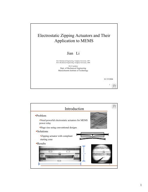
Electrostatic Zipping Actuators and TheirApplication to MEMSJian LiB.S. Mechanical Engineering, Tsinghua University, 1997M.S. Mechanical Engineering, Tsinghua University, 2000Ph.D CandidateDept. of Mechanical EngineeringMassachusetts Institute of Technology01/15/20041•ProblemIntroduction•Need powerful electrostatic actuators for MEMSpower relay•Huge size using conventional designs•Solutions•Zipping actuator with compliantstarting zone•Results~ 3 mm9 mm21
Contributions• Design: Starting zone to reduce the pull-in voltage• Numerical and analytical modeling: easy and accurate• Optimization of the system• Specified design for implementation in a relay• Fabrication and measurement of the actuator-relay• Wet-anisotropically-etched micro relay contact3Background: Electrostatic Actuators•Comb Drive•Force independentof stroke: largestroke•Very small force,large deflection•Parallel Plate•Conflictionbetween strokeand force•“Zipper”•Large force andlarge deflection•High voltage forpull_in42
F-D Curve of Three Electrostatic Actuators•Force-Displacement Character of the three actuators•With the same volume and same voltage, the “zipper” actuator achieves amuch larger force than comb drive an capacitor plate actuators•“Zipper” actuator is the only hope to secure milli Newtons of force with areasonable volumeForce (mN)12108642Parallel PlateComb DriveZipping Actutor00 20 40 60 80Displacement (µm)5Zipping Actuators: A SurveyAuthorShikidaActuationdirectionVerticalApplicationValveSize(mm 2 )5 * 5Force(mN)N/A(very small)Stroke(µm)220DivouxVerticalMirror0.8 * 0.80.16LegtenbergPerregauxShermanLateralLateralLateralN/AOpticalshutterFluidcontrol0.8 * 0.50.5 * 0.21 * 0.20.02N/A(very small)N/A(very small)3020100This thesisLateralRelay9 * 12 ~ 108063
Why Is It Hard ? (2)•Initial Design:•DRIE etch through•Attach the cantileverbeam to the double beam•Apply voltage betweenelectrode and the cantileverbeam.•Problem:•Minimum gap due toDRIE aspect ratio of ~5%•Very High pull-in voltagebecause of the gap, about250 V for a 15 µm thickand 4.5 mm long zippingbeam.Minimum GapUCantilever BeamCantilever Beam BeingElectrifiedDouble beam actuated by "Zipper"ElectrodeDouble Beam9Contributions• Design: Starting zone to reduce the pull-in voltage• Numerical and analytical modeling: easy and accurate• Optimization of the system• Specified design for implementation in a relay• Fabrication and measurement of the actuator-relay• Wet-anisotropically-etched micro relay contact105
Design: Compliant Starting Zone•To reduce the pull-involtage:•A compliant startingzone•Reciprocity: removematerial not needed andnot useful•The starting zonebends up when voltageis applied betweenelectrode and the beam•The cantilever beampulls-in and keepzipping at low voltageUActuatorCantilever Beamg minStartingCantilever a)b)Fixed electrodeBistable RelayBeam11Contributions• Design: Starting zone to reduce the pull-in voltage• Numerical and analytical modeling: easy and accurate• Optimization of the system• Specified design for implementation in a relay• Fabrication and measurement of the actuator-relay• Wet-anisotropically-etched micro relay contact126
Numerical Modeling: After “Pull-in”sLδdδmaxc(x)h 0yxsFleftLFrightδp(x)Model after pull-in•Numerical solutions•Eliminate varying B.C by adding parameterCantilever Beam Deflection profiles when the tip isconstrained at zero displacement(different voltages)ε bU0•Beam equation: EIy ''''( x) = p( x)=−2 s ≤ x ≤ L[ yx− cx+h ε ]2 ( ) ( )0/r2λ = 1− s / L15Analytical Modeling: After Pull-in•Approximation equation:654321F1/42E b εε0 rUhright~ ⎜d h0•Comparisons between analytical approximations and numerical results:Force (mN)7Device I, Numerical resultsDevice I, Analytical ResultsDevice II, Numerical ResultsDevice II, Analytical results⎛⎝⎞⎟⎠3/40100 120 140 160 180 200 220 240 260Voltage (V)168
Forces: Actuator vs. Switch Beam•Force-Displacementcurves of the actuatorand the double beam•> 160V is needed toactuate the doublebeam with ~ 3 mN ofcontact force•Can we change theforce-displacementcurve of the doublebeam withoutreducing the contactforce?Actuation force Fright (mN)20151050-50 20 40 60 80 100 120Displacement δ (µm)Relay with Uniform Thickness, FEA Actuator, U = 100 VActuator, U = 120 VActuator, U = 140 VActuator, U = 160 VForce-Displacement curves of the actuatorand the double beam17Contributions• Design: Starting zone to reduce the pull-in voltage• Numerical modeling: easier and more accurate• Optimization of the system• Specified design for implementation in a relay• Fabrication and measurement of the actuator-relay• Wet-anisotropically-etched micro relay contact189
Optimization of The Double Beam• Force ratio R = C(τ 0 ,τ 2 )• 1 δC( τ , τ ) = ( δI) Λ( τ , τ , w , w )∫0 2 0 2 0 2Start with constant I(x)Numerically calculate eigenfunctionsand eigenvalues [w i, τ i]choose δI = εΛ(τ 0, τ 2, w 0, w 2),satisfying thickness constraints.I(x) = I(x) +δINoSmall enough R?EndYes19Optimization of The Double Beam (II)• Actuationforce/Contact forceratio starts from~ 2.5:1.• Beam wasmodulated, forceratio was optimizedto ~1.5 :1.• ~ 120 V is neededto actuate the relay.Actuation force Fright (mN)20151050-50 20 40 60 80 100 120Displacement δ (µm)Relay with Uniform Thickness, FEAActuator, U = 100 VActuator, U = 140 V7.5 mNOptimized Relay, FEAActuator, U = 120 VActuator, U = 160 V4.5 mNForce-Displacement curves of the actuatorand the double beam2010
Contributions• Design: Starting zone to reduce the pull-in voltage• Numerical modeling: easier and more accurate• Optimization of the system• Specified design for implementation in a relay• Fabrication and measurement of the actuator-relay• Wet-anisotropically-etched micro relay contact21The Relaya)UUb)UUc)U~1.5 mmd)9 mm2211
Contributions• Design: Starting zone to reduce the pull-in voltage• Numerical modeling: easier and more accurate• Optimization of the system• Specified design for implementation in a relay• Fabrication and measurement of the actuator-relay• Wet-anisotropically-etched micro relay contact23Fabrication: Process Flow (1)Starting substrate: 4''DSP Si WaferSpin and pattern 10 µmof photoresistDRIE etch throughStrip photoresist inPiranha, RCA cleanGrow 0.2 µm ofthermal oxidevSilicon Silicon Oxide Photoresist2412
Fabrication: Process Flow (2)Starting substrate: 4''DSP Si WaferSpin and pattern 10 µmof photoresistDRIE etch throughStrip photoresist inPiranhaBond shadow waferand device wafer, etchoxide selectivelySeparate wafers, cleandevice wafer in PiranhaSilicon Silicon Oxide Photoresist25Fabrication: Process Flow (3)Starting substrate: 4''Pyrex 7740 wafer, 500mm thickDeposite 0.005 mm Ti,0.03 mm CrPattern Cr in CR-7Etch Pyrex 50 mm in49% HFBond device wafer toPyrex wafer at 800 Vand 350 degree CSputter Au on relaycontactsSilicon Silicon Oxide PhotoresistTitaniumChromiumGold2613
Fabrication: Transparency Mask• Transparency maskfor device wafer:• Much faster andmuch cheaper• Low resolution: 3-4µm• Electrostatic force isvery sensitive to therecess at electrode• Print the mask 10times larger and use10:1 stepper toshrink it downDevice made using Transparency MaskElectrodeCantilever BeamElectrodeCantilever BeamDevice made using transparencymask and 10:1 Stepper27Fabrication Results: Overview4513 3 7128500 µm2 1 11 6109122814
Measurement: Pull_in of the Starting Zone• The starting beam bendsup and closes the gapbetween zipper beam andfixed electrode• Pull-in at 75V• 140 V. Zipper beamcollapse to the fixedelectrode, relay is closed29Force Measurement12108Force (mN)6420-2Flextester-40 20 40 60 80 100 120Displacement δ (µm)Relay FEAActuator Numerical Simulation at 140VRelay FEA (Adjusted model)Relay ExperimentalActuator Experimental at 140V3015
A Bipolar Drive to Avoid StictionDQ1k5k2N3904InputSignalDCC74LS74+5V74LS74QQQ5k5k+15V1k+15V4k2N39042N39041k+15V2N39045k5k+100V TopElectrodeSTP6NB50+100VSTP6NB50BottomElectrode+100V Middle5k ElectrodeSTP6NB50InputSignalTopElectrodeBottomElectrodeMiddleElectrode• Change polarity everytwo actuation cyclestttt31Relay Actuated by Zipping Actuator• > 40 millions of life cycleswere achieved• Maximum toggling speed:160 Hz• Shortest excitation pulse:400 µsClick for a movie3216
Switching Time• Contact bouncetime ~ 0.5 ms• Switching time ~ 3ms33Contributions• Design: Starting zone to reduce the pull-in voltage• Numerical modeling: easier and more accurate• Optimization of the system• Specified design for implementation in a relay• Fabrication and measurement of the actuator-relay• Wet-anisotropically-etched micro relay contact3417
DRIE-etched Relay Contacts• Relay contacts• Vertical sidewalls• Sputter Au: lowefficiency.• Sidewall/surfacethickness ratio = 1/9• Contact resistance:~1 Ω35KOH-etched Relay Contacts: Design3618
KOH-etched Relay Contacts: Experiments37KOH-etched Relay Contacts: Tests• Sputter Au: high efficiency.• Sidewall/surface thickness = 1/1.4• Very low contact resistance: ~ 50 mΩ3819
Proposed Full Relay Process Flow39Conclusions and Future Work• Conclusions:• Design, modeling, optimization, fabrication andmeasurement of an actuator-relay system• Develop wet-anisotropically-etched relay contacts• Future work:• Combine the actuator and the KOH-etchedcontacts• Vertically moving zipping actuators4020
Acknowledgements• Advisors: Prof. Alexander Slocum, Prof. Jeffrey Lang,Prof. Michael Brenner (Harvard University)• Discussion (PERG): Dr. Jin Qiu, Dr. Joachim Sihler• Fabrication (at MTL): Kurt Broderick, Dennis Ward, PaulTierney, Linvhu Hol, Dr. Hongwei Sun …• Testing (at ABB Research): Dr. Ralf Struempler, Dr. SamiKotilainen, Dr. Jan-henning Fabian, Eric Wapelhorst,Jeff Renaud414221
43Actuator Beam Profile15.78 µmDRIE Etchdirection13.00 µm12.78 µm285.8 µm15.24 µm4422
•Beam equation:( E I w'')''+ T w''= 0Optimization: Algorithm (1)( EIδ w'')'' + Tδw'' =−δTw'' −( EδIw'')''∫i i i i i i•Fredholm alternative:( δ δ )Tw'' + ( E Iw'')'' wdx=0i i i iiδ Ti=− ∫ ∫w ( EδI w '')'' dxw '' w dx•Cost function variation:iii∫δ T = Eδ⎡ ∞2dC ( w '')⎤δ iC( { Ti}) = ∫ δ I ⎢∑⎥ = I ( T, )2iwii 1 dTi ( wi')∫ δ Λ⎢ =⎥⎣ ∫ ⎦iI ( wi'')2∫ ( wi')2dxdx45•Beam equation:•Transition stateOptimization: Algorithm (2)2( EI( w− w0)'') '' + τ w'' = fδ( x−L/ 2)w ( )t=Γ w0 x + Awn800600400Γ = (1 − ( τ / τ∆*= 1−ΓR*= =*2 −10) )( 1−Γ)∆2−∆ 2 −(1 −Γ)2( τ2 τ0)=2 − ( τ τ )2 02force200∫δ T = Eδ-2000iI ( wi'')2∫ ( wi')2dxdx-4000 0.5 1∆displacement *1.5 24623
Analytical Analysis (1)•Beam equation:EIy ''''( x) = p( x)= −Γ[ y( x)+ β ] 2⇒sLδ⎧ 1 LFleft= ⋅ −px ( ) ⋅[ ( L−s)− xdx ]⎪ L−s∫s⇒ ⎨1 L⎪ Fright= ⋅ p( x) ⋅( x−s)dx⎪⎩L−s∫sc(x)dδmaxh 048•Near x = sΓy( x) =− ( x− s) + A( x−s)224EIβ4 3yxsFleftLFrightδ⇒F = EIy '''( s) = 6EIAleftp(x)47βF* * 3 * 4= = ⋅ − − −224EIβ⎪ ⎬⎪leftΓ ⎫yx ( ) A( x s) ( x s)= 6EIA⎭Analytical Analysis (2)•Assume most of the force comes from s
•Far from x = sy( x) B( x s)Analytical Analysis (3)⇒Γ~ 2 EIβEIβ( x − s)~( )Γ2*= − B ( x − s) 223* 1/4⎫⎪⎬⎪⎪⎭⇒ΓB ~EIβd B L s⎫⎪⎬⎪2= ( − ) ⎭⇒⇒1/4⎛EIβ⎞ ⎫L − s ~ ⎜ ⎟ d⎝ Γ ⎠ ⎪ ⎬1 EIΓFright~⎪L−s β ⎪⎭⇒Fright1~ ( EI)d1/4⎛ Γ ⎞⎜ ⎟⎝β⎠3/4⇒F1/42E b εε0 rUhright~ ⎜d h0⎛⎝⎞⎟⎠3/449Analytical Analysis (4)Force (mN)765432Device I, Numerical resultsDevice I, Analytical ResultsDevice II, Numerical ResultsDevice II, Analytical results10100 120 140 160 180 200 220 240 260Voltage (V)5025