
Create successful ePaper yourself
Turn your PDF publications into a flip-book with our unique Google optimized e-Paper software.
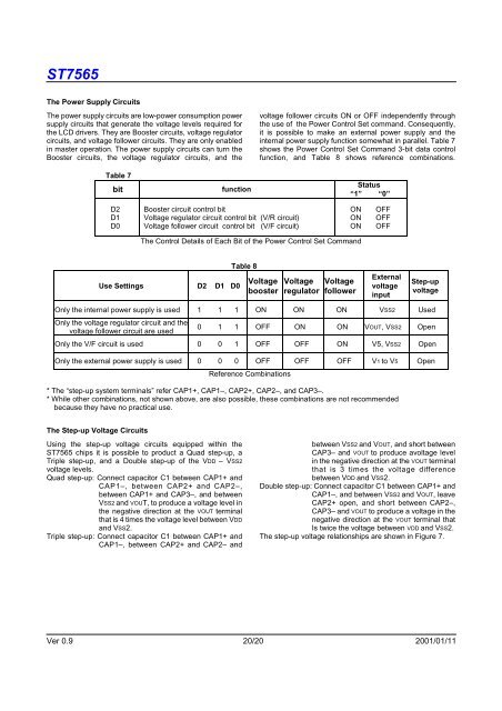
<strong>ST7565</strong>The Power Supply CircuitsThe power supply circuits are low-power consumption powersupply circuits that generate the voltage levels required forthe LCD drivers. They are Booster circuits, voltage regulatorcircuits, and voltage follower circuits. They are only enabledin master operation. The power supply circuits can turn theBooster circuits, the voltage regulator circuits, and thevoltage follower circuits ON or OFF independently throughthe use of the Power Control Set <strong>com</strong>mand. Consequently,it is possible to make an external power supply and theinternal power supply function somewhat in parallel. Table 7shows the Power Control Set Command 3-bit data controlfunction, and Table 8 shows reference <strong>com</strong>binations.Table 7bitfunctionStatus“1” “0”D2D1D0Booster circuit control bitVoltage regulator circuit control bit (V/R circuit)Voltage follower circuit control bit (V/F circuit)ONONONOFFOFFOFFThe Control Details of Each Bit of the Power Control Set CommandUse Settings D2 D1 D0Table 8VoltageboosterVoltageregulatorVoltagefollowerExternalvoltageinputStep-upvoltageOnly the internal power supply is used 1 1 1 ON ON ON VSS2 UsedOnly the voltage regulator circuit and thevoltage follower circuit are used0 1 1 OFF ON ON VOUT, VSS2 OpenOnly the V/F circuit is used 0 0 1 OFF OFF ON V5, VSS2 OpenOnly the external power supply is used 0 0 0 OFF OFF OFF V1 to V5 OpenReference Combinations* The “step-up system terminals” refer CAP1+, CAP1–, CAP2+, CAP2–, and CAP3–.* While other <strong>com</strong>binations, not shown above, are also possible, these <strong>com</strong>binations are not re<strong>com</strong>mendedbecause they have no practical use.The Step-up Voltage CircuitsUsing the step-up voltage circuits equipped within the<strong>ST7565</strong> chips it is possible to product a Quad step-up, aTriple step-up, and a Double step-up of the VDD – VSS2voltage levels.Quad step-up: Connect capacitor C1 between CAP1+ andCAP1–, between CAP2+ and CAP2–,between CAP1+ and CAP3–, and betweenVSS2 and VOUT, to produce a voltage level inthe negative direction at the VOUT terminalthat is 4 times the voltage level between VDDand VSS2.Triple step-up: Connect capacitor C1 between CAP1+ andCAP1–, between CAP2+ and CAP2– andbetween VSS2 and VOUT, and short betweenCAP3– and VOUT to produce avoltage levelin the negative direction at the VOUT terminalthat is 3 times the voltage differencebetween VDD and VSS2.Double step-up: Connect capacitor C1 between CAP1+ andCAP1–, and between VSS2 and VOUT, leaveCAP2+ open, and short between CAP2–,CAP3– and VOUT to produce a voltage in thenegative direction at the VOUT terminal thatIs twice the voltage between VDD and VSS2.The step-up voltage relationships are shown in Figure 7.Ver 0.9 20/20 2001/01/11