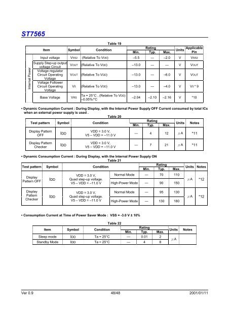
<strong>ST7565</strong>Internal PowerItem Symbol ConditionTable 19RatingMin. Typ. Max.Units ApplicablePinInput voltage VSS2 (Relative To VDD) –5.5 — –2.0 V VSS2Supply Step-up outputvoltage CircuitVoltage regulatorCircuit OperatingVoltageVoltage FollowerCircuit OperatingVoltageBase VoltageVOUT (Relative To VDD) –13.0 — — V VOUTVOUT (Relative To VDD) –13.0 — –6.0 V VOUTV5 (Relative To VDD) –13.0 — –4.0 V V5 * 9VRSTa = 25°C , (Relative To VDD)–0.05%/°C–2.04 –2.10 –2.16 V *10• Dynamic Consumption Current : During Display, with the Internal Power Supply OFF Current consumed by total ICswhen an external power supply is used .Table 20RatingTest pattern Symbol ConditionUnits NotesMin. Typ. Max.Display PatternOFFIDDVDD = 3.0 V,V5 – VDD = –11.0 V— 4 12 μA *11Display PatternCheckerIDDVDD = 3.0 V,V5 – VDD = –11.0 V— 7 21 μA *11• Dynamic Consumption Current : During Display, with the Internal Power Supply ONTable 21RatingTest pattern Symbol ConditionMin. Typ. Max.DisplayPattern OFFIDDVDD = 3.0 V,Normal Mode — 70 110Quad step-up voltage.V5 – VDD = –11.0 V High-Power Mode — 90 150Units NotesμA *12DisplayPatternCheckerIDDVDD = 3.0 V,Normal Mode — 95 130Quad step-up voltage.V5 – VDD = –11.0 V High-Power Mode — 130 180μA *12• Consumption Current at Time of Power Saver Mode : VSS = -3.0 V ± 10%Table 22Item Symbol ConditionRatingMin. Typ. Max.Sleep mode IDD Ta = 25°C — 0.01 2Standby Mode IDD Ta = 25°C — 4 8UnitsμANotesVer 0.9 48/48 2001/01/11
<strong>ST7565</strong>• The Relationship Between Oscillator Frequency fOSC, Display Clock Frequency fCL and the Liquid Crystal FrameRate Frequency fFRTable 23Item fCL fFR1/65 DUTY1/49 DUTY1/33 DUTY1/55 DUTYUsed internal oscillator circuit fOSC / 4 fOSC / (4*65)Used external display clock External input (fCL) fCL / 260Used internal oscillator circuit fOSC / 4 fOSC / (4*49)Used external display clock External input (fCL) fCL / 196Used internal oscillator circuit fOSC / 8 fOSC / (8*33)Used external display clock External input (fCL) fCL / 264Used internal oscillator circuit fOSC / 4 fOSC / (4*55)Used external display clock External input (fCL) fCL / 2201/53 DUTYUsed internal oscillator circuit fOSC / 4 fOSC / (4*53)Used external display clock External input (fCL) fCL / 212(fFR is the liquid crystal alternating current period, and not the FR signal period.)References for items market with **1 While a broad range of operating voltages is guaranteed, performance cannot be guaranteed if there are suddenfluctuations to the voltage while the MPU is being accessed.*2 The operating voltage range for the VDD system and the V5 system is. This applies when the external power supply isbeing used.*3 The A0, D0 to D5, D6 (SCL), D7 (SI), RD (E), WR (R/W), CS1, CS2, CLS, CL, FR, M/S, C86, P/S, DOF, RES, IRS, and HPMterminals.*4 The D0 to D7, FR, FRS, DOF, and CL terminals.*5 The A0, RD (E), WR (R/W), CS1, CS2, CLS, M/S, C86, P/S, RES, IRS, and HPM terminals.*6 Applies when the D0 to D5, D6 (SCL), D7 (SI), CL, FR, and DOF terminals are in a high impedance state.*7 These are the resistance values for when a 0.1 V voltage is applied between the output terminal SEGn or COMn and thevarious power supply terminals (V1, V2, V3, and V4). These are specified for the operating voltage (3) range.RON = 0.1 V /ΔI (Where ΔI is the current that flows when 0.1 V is applied while the power supply is ON.)*8 See Table 23 for the relationship between the oscillator frequency and the frame rate frequency.*9 The V5 voltage regulator circuit regulates within the operating voltage range of the voltage follower.*10 This is the internal voltage reference supply for the V5 voltage regulator circuit. In the <strong>ST7565</strong>-0A , the temperature rangeapproximately –0.15%/°C.*11, 12 It indicates the current consumed on ICs alone when the internal oscillator circuit and display are turned on.The <strong>ST7565</strong> is 1/9 biased. Does not include the current due to the LCD panel capacity and wiring capacity.Applicable only when there is no access from the MPU.*12 It is the value on a <strong>ST7565</strong>-0A having the VREG temperature gradient is –0.15%/°C when the V5 voltage regulatorinternal resistor is used.Ver 0.9 49/49 2001/01/11