
You also want an ePaper? Increase the reach of your titles
YUMPU automatically turns print PDFs into web optimized ePapers that Google loves.
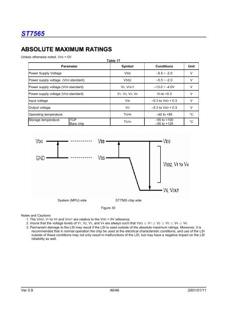
<strong>ST7565</strong>ABSOLUTE MAXIMUM RATINGSUnless otherwise noted, VSS = 0VTable 17Parameter Symbol Conditions UnitPower Supply Voltage VSS –5.5 ~ -2.0 VPower supply voltage (VDD standard) VSS2 –5.5 ~ -2.0 VPower supply voltage (VDD standard) V5, VOUT –13.0 ~ -4.0V VPower supply voltage (VDD standard) V1, V2, V3, V4 V5 to +0.3 VInput voltage VIN –0.3 to VDD + 0.3 VOutput voltage VO –0.3 to VDD + 0.3 VOperating temperature TOPR –40 to +85 °CStorage temperatureTCPBare chipTSTR–55 to +100–55 to +125°CSystem (MPU) side<strong>ST7565</strong> chip sideFigure 30Notes and Cautions1. The VSS2, V1 to V5 and VOUT are relative to the VDD = 0V reference.2. Insure that the voltage levels of V1, V2, V3, and V4 are always such that VDD ≧ V1 ≧ V2 ≧ V3 ≧ V4 ≧ V5.3. Permanent damage to the LSI may result if the LSI is used outside of the absolute maximum ratings. Moreover, it isre<strong>com</strong>mended that in normal operation the chip be used at the electrical characteristic conditions, and use of the LSIoutside of these conditions may not only result in malfunctions of the LSI, but may have a negative impact on the LSIreliability as well.Ver 0.9 46/46 2001/01/11